Label-free Immobilization of Nano-particles
on Silicon based Electrodes for Single-biomolecule Studies
Ch. Wenger
1
, X. Knigge
2
, M. Fraschke
1
, D. Wolansky
1
, P. Kulse
1
, U. Kaletta
1
, A. Wolff
1
, W. Mehr
1
,
E.-M. Laux
2
, F. F. Bier
2
and R. Hölzel
2
1
IHP GmbH – Leibniz Institute for Innovative Microelectronics, Im Technologiepark 25, 15236 Frankfurt (Oder), Germany
2
Fraunhofer Institute for Biomedical Engineering IBMT, Branch Potsdam-Golm, Potsdam, 14476, Germany
Keywords: Dielectrophoresis, Nanoelectrodes, Biosensing.
Abstract: Dielectrophoresis (DEP) is an established method for the spatial manipulation of microscopical particles.
We demonstrate the temporal and permanent immobilization of polystyrene nanoparticles and protein
molecules with sizes ranging from 4 nm to 500 nm. For this, regular arrays of silicon based nanoelectrodes
were developed with tip diameters of 10 nm and 50 nm. No chemical modifications of molecules, particles
or surfaces were needed. This opens up potentially important applications of DEP in biosensing and cell
research.
1 INTRODUCTION
There is a growing need in lab-on-a-chip systems
and similar biodevices for spatial manipulation of
nanoparticles like concentrating, immobilizing,
orientating and aligning. The manipulation should be
performed on a large number of objects
simultaneously. AC electrokinetic methods like DEP
have been successfully applied for some decades by
exploiting alternating electric fields between
microelectrodes. In the case of non-uniform fields,
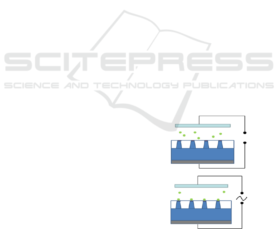
polarizable particles get immobilized on top or at the
edges of the electrodes, as illustrated in Fig. 1.
So far, most of the research work performed on
DEP has been done by using metal electrodes
(Widdershoven 2010, Martinez-Duarte 2012). The
continuous downscaling of CMOS minimum feature
sizes provides great opportunities. By adapting the
typical electrode dimensions to the objects' size, it
has become possible to manipulate even single
objects like viruses and proteins on metal electrodes
(Yamamoto 2007, Pethig 2010, Diao 2011 Nakano
2013). Nevertheless, the dimensions of CMOS metal
electrodes are still in the range of 100 nm (ITRS
2012 update), which doesn’t fit to nanoparticles like
proteins with diameters of less than 10 nm (Hölzel
2005). A modern approach to optimize the
interaction between particles and electrodes is the
use of doped triangular shaped silicon as electrode
material.
Figure 1: Dielectrophoresis: Schematic illustration of the
experimental setup. a) Nanoobjects are suspended in water
b) By applying inhomogeneous AC electric fields,
electrical forces act on polarizable particles. These forces
lead to a local particle accumulation. Distance between top
electrode and electrode surface is about 100 µm.
2 EXPERIMENTAL
Cone-shaped nanoelectrodes were fabricated in a
a)
b)
176
Wenger C., Knigge X., Fraschke M., Wolansky D., Kulse P., Kaletta U., Wolff A., Mehr W., Laux E., Bier F. and Hölzel R..
Label-free Immobilization of Nano-particles on Silicon based Electrodes for Single-biomolecule Studies.
DOI: 10.5220/0004888101760180
In Proceedings of the International Conference on Biomedical Electronics and Devices (BIODEVICES-2014), pages 176-180
ISBN: 978-989-758-013-0
Copyright
c
2014 SCITEPRESS (Science and Technology Publications, Lda.)
standard CMOS process line by using reactive ion
etching (RIE) process techniques (Mehr 1996). The
minimum tip radius is about 1.5 nm. The electrodes
are embedded in a SiO
2
matrix and the diameter on
top of the tips can be increased by chemical
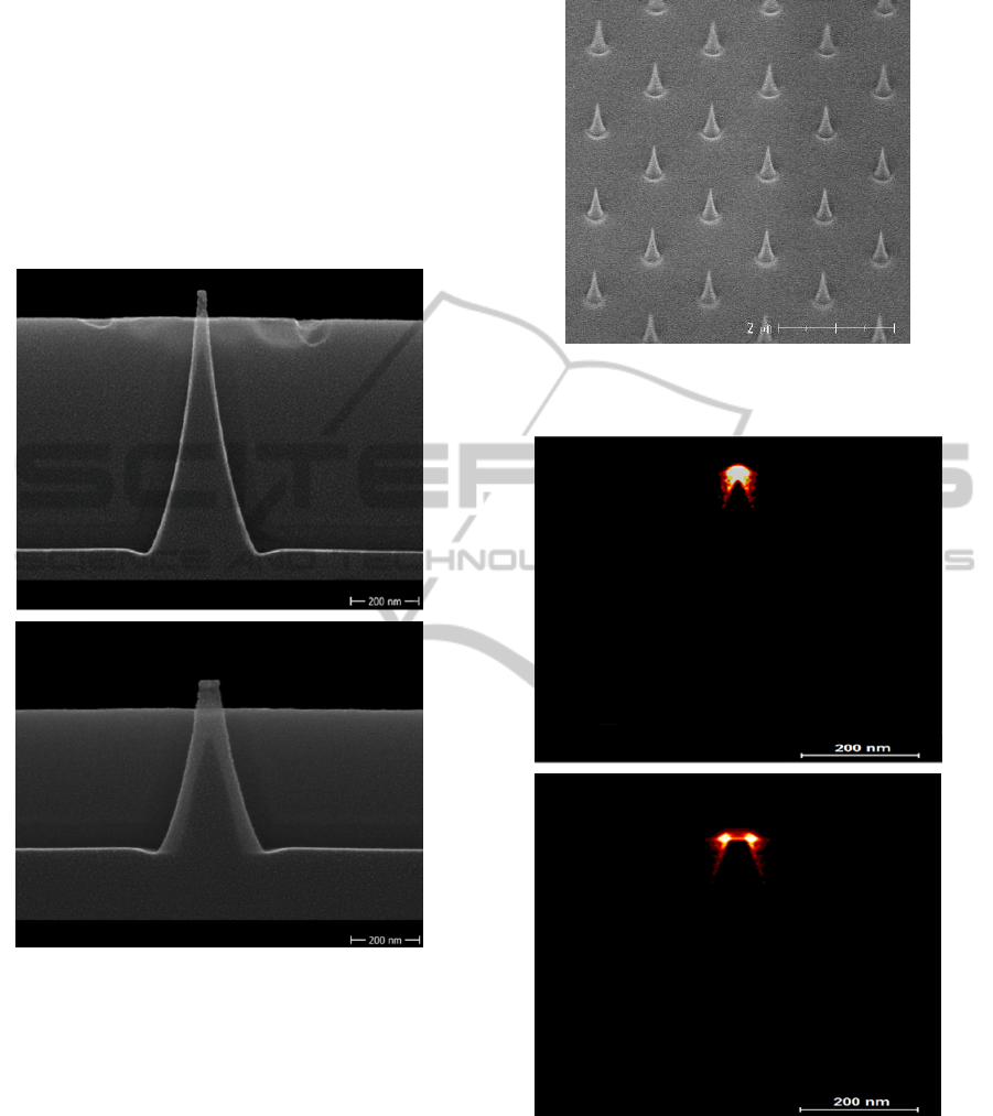
mechanical polishing (CMP), as shown in Fig. 2.
The process flow is completed with silicidation of
the tip surface (CoSi). The total number of
electrodes amounts to about 100.000 per array (Fig.
3).
Figure 2: Cross-sectional scanning electron microscope
(SEM) image of plasma etched electrodes with a) 10 nm
and b) 50 nm diameter at the top of the silicon based
electrodes.
The DEP force acting on the particles is directed
along the gradient of the electric field. Therefore, the
implementation of a steep electric field gradient is
required to maximize the DEP force acting on the
particles.
The simulation (Fig. 4) shows the largest electric
field gradient and, hence, the strongest DEP force on
top of the 10 nm tip electrode. For the 50 nm top
surface, the strongest force is localized at the edges
of the electrode, leading to a ring-like alignment.
Obviously, for single molecule immobilization, the
tip diameter has to be minimized.
Figure 3: SEM image of the plasma etched nanoelectrode
array.
Figure 4: Simulation of the electric field gradient grad |E|
2
above the nanoelectrodes with a) 10 nm and b) 50 nm tip
diameter. Maximum field gradient (white) is close to the
tip.
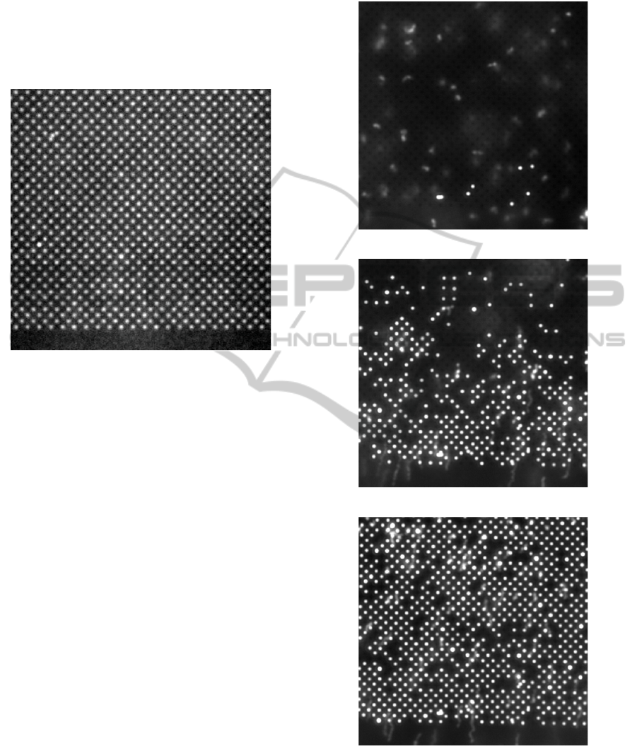
To demonstrate the permanent immobilization of a
biomolecule on an electrode array (Fig. 5), we used
the fluorescently labeled bovine serum albumin
(BSA), which is a protein of prolate ellipsoidal
shape (14 nm x 4 nm x 4 nm (Squire 1968)).
a)
a)
b
)
b
)
Label-freeImmobilizationofNano-particlesonSiliconbasedElectrodesforSingle-biomoleculeStudies
177
Typically, these experiments were carried out at
about 10 kHz with 5 to 10 V
RMS
for periods of some
seconds to minutes. By choosing the optimum
operating conditions, the immobilization of
nanobeads with diameters of 200 nm is finalized
within a few minutes, as illustrated in Fig. 6.
Figure 5: DEP field induced immobilization of the
fluorescently labeled protein BSA on nanoelectrodes after
field application of 10 kHz and 7 V
RMS
for 10 min.
The distribution of fluorescence intensity of
immobilized nanobeads with diameters of 20 nm on
electrode tips with diameters of 50 nm is quite
broad, as shown in Fig. 7a. That means, ensembles
of numerous nanobeads were immobilized on each
electrode tip.
However, by applying this system to objects that
were slightly larger than the electrode tips, we were
able to achieve a proper 1:1 ratio between particles
and tips, as illustrated in Fig. 7b. That means,
exactly one nanobead was placed on each electrode
tip.
This opens a completely novel approach to
single-molecule investigations on large ensembles.
This deterministic control of local particle numbers
in aqueous solutions demonstrates the importance of
reducing the typical electrode dimensions to 10 nm
and less.
In addition, one has to consider that alternating
electric fields lead to Joule heating in the liquid
medium (Seger-Sauli 2005). Local temperature
raises could cause thermal stress, cell damages and
protein denaturing. Therefore, we measured the
heating of the medium close to the electrodes at
1 MHz and 9 V
RMS
as a function of electrode
diameter. The temperature variation was detected by
exposing the thermo-dependent fluorescent dye
a
)
b)
c)
Figure 6: Top view microscopic images through the
transparent top electrode of 200 nm fluorescent
polystyrene nanospheres in water on the nanoelectrode
array. a) Before field application, b) after field application
at 17 kHz and 8 V
RMS
for 12 s and c) after 60 s field
application.
BIODEVICES2014-InternationalConferenceonBiomedicalElectronicsandDevices
178
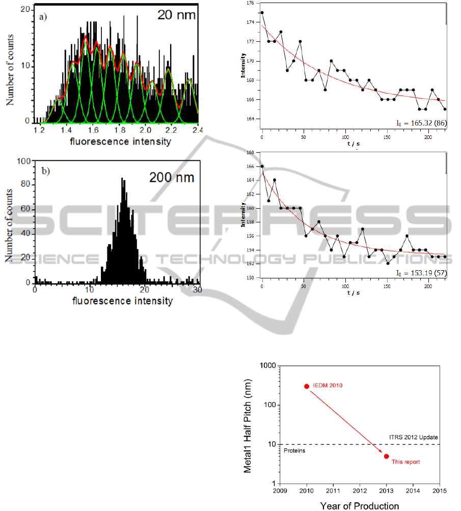
Figure 7: Fluorescence intensity distribution of dielectro-
phoretically immobilized polystyrene nanospheres. Bead
diameters are a) 20 nm and b) 200 nm. Electrode diameter
is 50 nm. a) For particles smaller than the electrodes,
accumulation of approx. 1 to 15 particles per electrode tip
occurs. b) 200 nm spheres are immobilized as singles.
rhodamine B to the test set-up. Its fluorescence
intensity decreases with temperature by about -
1.2%/K
As shown in Fig. 8, temperature rises within
220 s by 5 °C for 10 nm tip diameter and by 6 °C for
50 nm tip diameter. This improvement by smaller
electrodes can be explained by the corresponding
reduction of the volume carrying high current
densities. Above that, the increased surface-to-
volume ratio enhances heat dissipation from the
electrodes.
As illustrated in Fig. 9, the proposed silicon-
based technology for immobilization of nanometer
sized molecules by cone-shaped nanoelectrodes
opens a new CMOS compatible platform for the
analysis of single proteins and their functions.
Figure 8: Intensity characteristics of the thermo-dependent
fluorescence of rhodamine B in order to evaluate the
temperature increase in the liquid medium above the
nanoelectrodes with a) 10 nm and b) 50 nm tip diameter.
Figure 9: CMOS Metal1 half pitch roadmap (ITRS 2012)
compared to typical dimensions of proteins.
3 CONCLUSIONS
We demonstrated the electrically controlled
immobilization of biomolecules and nanospheres
using silicon based nanoelectrode arrays. The
nanoelectrodes with tip sizes of 10 and 50 nm were
a)
b)
Label-freeImmobilizationofNano-particlesonSiliconbasedElectrodesforSingle-biomoleculeStudies
179

fabricated by reactive ion etching (RIE) techniques
in a standard CMOS process line. Electric field
distributions were calculated. Temperature changes
within the device were determined by optical
microscopy to about 5 °C, which is well compatible
with biomedical applications.
Nanospheres with diameters of 20 nm and
200 nm suspended in water were immobilized at the
electrode tips. For particles larger than the
electrodes, immobilization of single objects was
demonstrated. The procedure was performed within
a few tens of seconds. Any chemical modifications
of suspended particles, dissolved molecules or
surfaces could be avoided.
The demonstrated use of silicon based
nanoelectrode arrays for the dielectrophoretic
immobilization of particles and molecules opens a
novel way for nanoparticle separation and for the
preparation of miniaturized biosensors.
ACKNOWLEDGEMENTS
This work was supported by the grant from the
federal state of Brandenburg and the European
Regional Development Fund.
REFERENCES
Widdershoven, R., Van Steenwinckel, D., Überfeld, J.,
Merelle, T., Suy H., Jedema, F., Hoofman, R., Tak, C.,
A. Sedzin, B. Cobelens, E. Sterckx, R. van der Werf,
K. Verheyden, M. Kengen, F. Swartjes, F. Frederix
IEDM Proceedings 2010.
Martinez-Duarte, R., Electrophoresis 2012, 33, 3110.
Yamamoto, T.; Fujii, T.; Nanotechnology 2007, 18,
495503.
Pethig, R., Biomicrofluidics 2010, 4, 022811.
Diao, J. J., Cao Q., AIP Advances 2011, 1, 012115.
Nakano, A., Ros, A., Electrophoresis 2013, 34, 1085.
Hölzel, R., Calander, N., Chiragwandi, Z., Willander, M.,
Bier, F., Phys. Rev. Lett. 2005, 128102.
Mehr, W., Wolff, A., Frankenfeld, H., Skaloud, T.,
Höppner, W., Bugiel, E., Lärz, J., Hunger, B., Microel.
Engineering 1996, 30, 395-398.
Erickson, H. P, Biological Proc. Online 2009, 11, 32.
Squire, P.G., Moser, P., O’Konski, C.T., Biochemistry,
1968, 7, 4261.
Seger-Sauli, U., Panayiotou, M., Schnydrig, S., Jordan,
M., Renaud, P., Electrophoresis 2005, 26, 2239.
BIODEVICES2014-InternationalConferenceonBiomedicalElectronicsandDevices
180
