
PZT AND PNZT-BASED THIN FILM CAPACITORS AND
TRANSMISSION LINES FOR MICROWAVE INTEGRATED
CIRCUIT APPLICATIONS
Z. Awang and S. Sulaiman
Microwave Technology Centre, University Technology MARA, 40450 Shah Alam, Malaysia
zaiki.awang@gmail.com, anisafiq2@yahoo.com
Keywords: Thin film capacitor, co-planar waveguide transmission line, PZT, PNZT, thin dielectric films, monolithic
microwave integrated circuits.
Abstract: Ferroelectric materials have superior dielectric properties but the processing conditions of thin ferroelectric
films influence their dielectric properties and thus affect the performance of devices which employ them. A
detailed characterization is carried out for lead zirconate titanate (PZT) and lead niobate zirconate titanate
(PNZT) thin films in this work by employing planar-circuit structures. The films were applied to built
microwave capacitors and co-planar waveguide transmission lines. S-parameter measurements were
performed from 40 MHz to 20 GHz using wafer probes in conjunction with a vector network analyzer. The
results show the loss tangent and relative permittivity of the films vary with frequency, with typical
permittivity values of the order of 110 to 350 and 200 to 780 for PZT and PNZT, respectively, over the said
frequency range. The investigation revealed the effect of dielectric polarization of the films over the broad
frequency range. The transmission lines showed acceptable insertion losses of the order of 17 dB from 5 to
20 GHz for lines of length 100 µm and width 5 µm fabricated on PNZT films 1 µm thick. These figures
demonstrate the feasibility of using thin ferroelectric films as a new substrate material for monolithic
microwave integrated circuits (MMIC).
1 INTRODUCTION
Ferroelectric materials are popular due to their
superior dielectric properties characterized by their
high dielectric constant and polarization values. The
review made by (Setter et. al., 2006) discussed their
dielectric properties and represented the state of the
art development of the material - the domain
structure and their effects on relative permittivity
and loss, and their implication in micro-systems and
high frequency device applications .
Lead zirconate titanate (PZT) and lead niobate
zirconate titanate (PNZT) belong to the family of
ferroelectric materials. Both are known for their high
dielectric constant as well as their superior
perovskite characteristics useful for high capacitor
density applications (Dimos and Mueller, 1998,
Riemens et. al. 2003 and Haccart et. al., 2006). With
the addition of a dopant such as Nb, the PZT can
demonstrate higher dielectric constant and promote
larger perovskite crystals, as well as increased film
resistivity (Souza et.al., 2004). The addition of Nb
also influences the film characteristics such as
microstructure, as well as the electrical properties.
Also, there is correlation between internal electric
field and ‘self polarization’ of the films that
increases with Nb concentration.
Souza et.al., 2004 found that the enhancement of
the piezoelectric and ferroelectric properties of
PNZT is possible with careful control of the
crystallographic orientation of the polycrystalline
films or growing the epitaxial films with preferred
orientation. Their study also investigated the film
thickness effects on the ferroelectric and
piezoelectric properties of PNZT thin films.
In our work, PZT and PNZT thin films prepared
differently were utilized to explore their microwave
95
Awang Z. and Sulaiman S.
PZT AND PNZT-BASED THIN FILM CAPACITORS AND TRANSMISSION LINES FOR MICROWAVE INTEGRATED CIRCUIT APPLICATIONS.
DOI: 10.5220/0004785800950103
In Proceedings of the Second International Conference on Telecommunications and Remote Sensing (ICTRS 2013), pages 95-103
ISBN: 978-989-8565-57-0
Copyright
c
2013 by SCITEPRESS – Science and Technology Publications, Lda. All rights reserved
properties. The films were studied over two types of
applications – as thin film metal-insulator-metal
(MIM) capacitors, and as a new substrate material
for the construction of co-planar waveguides. The
principal motivation of this work was to exploit the
high dielectric constant of these films to reduce the
size of capacitors and transmission lines, two
components which traditionally take up large area of
MMIC. Thus using these ferroelectric films offer the
potential of reducing the size of MMICs, leading to
wireless systems having more efficient power
consumption.
Two capacitor test structures of 2500 μm
2
area
were fabricated on the films and measured by
employing the planar circuit technique. The
measurement was performed using Cascade
Microtech wafer probes and a vector network
analyzer with short-open-load (SOL) calibration
technique. The measurements were carried out over
a wide frequency range of 40 MHz to 20 GHz which
are suitable for MMIC applications. The
capacitance, loss tangent and relative permittivity of
the films were then extracted from the experimental
data. From the analysis, behavior of dielectric
polarization of PNZT and PZT over a broad
frequency range was deduced.
Various transmission lines were then constructed
in co-planar form with both films acting as the
substrate. The novelty of this work is to show the
feasibility of using ferroelectric materials as the
substrate for MMIC. This paper reports results of
further investigations of our previous work, which
has been extended to include tests on the various
transmission line structures.
2 METHODOLOGY
The films were prepared using standard methods
compatible with MMIC processing. The objectives
of the experimental work made were to two-fold: to
analyze the capacitance, loss tangent and their
relative permittivity at microwave frequencies, and
to measure the insertion loss of the films by
analyzing the transmission lines constructed out of
these films.
2.1 Sample Preparation
The PZT and PNZT samples were categorized based
on the method of deposition, doping, dielectric
thickness, orientation, crystallinity and grain size
obtained from the X-ray diffraction (XRD). The
PNZT films were grown using metal organic
deposition to give films of 1 µm thick, while the
PZT was prepared with RF sputtering with
thicknesses of the order of 0.5 µm. The PNZT films
were tetragonal (20/80) and doped with 4 % Nb,
while the PZT films were (50/50) cubic. The top
metallization layers of the capacitor structures were
Ti, while Pt was used as bottom electrodes.
2.2 Device Fabrication
The fabrication processes used are compatible with
semiconductor processing, details of which are
reported earlier (Bakar et. al., 2008). The fabrication
for PNZT sample was modified slightly due to the Pt
etchant which attacked the PMMA photoresist used.
For this sample, the capacitor test structures were
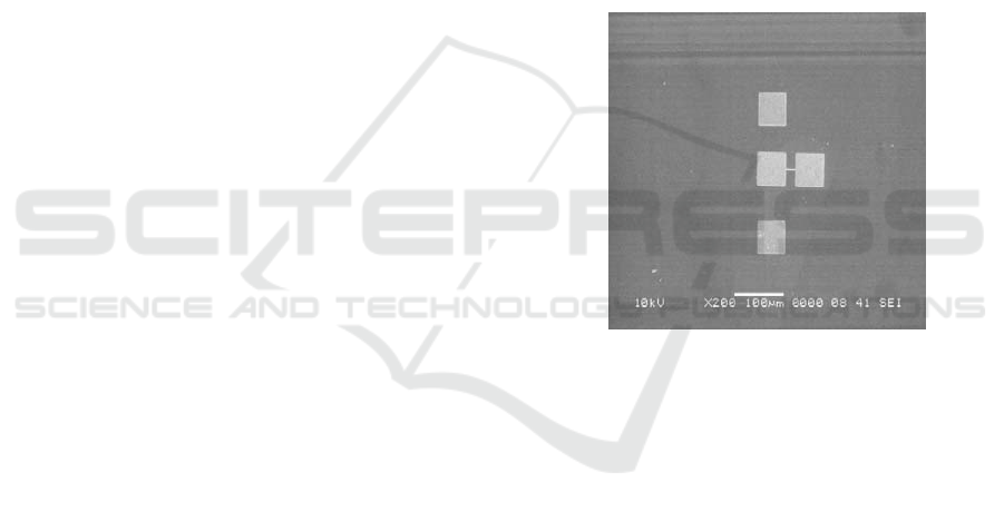
delineated after the Pt layer was removed. Figure 1
shows the capacitor prototype with area 50 µm × 50
µm.
Figure 1: A typical thin film capacitor test structure
constructed in this work, with ground-signal-ground
(GSG) pads on the left for wafer probing.
2.3 Measurement
High frequency measurements were carried out on
the capacitor using on-wafer probe and vector
network analyzer (VNA). The SOL one-port
calibration technique was performed for the
capacitance measurements, while SOLT was
employed to calibrate the two-port transmission line
structures to minimize measurement errors due to
parasitics (WinCal 3.2 User Guide, 2000). The Open
standard in SOL was obtained by lifting the probe at
least 0.25 mm in air, while the Short and 50
standards were provided by the manufacturer
impedance standard substrate (ISS). The probe tip
placements were ensured to be consistent to achieve
repeatable measurements and calibrations. The short
standard defines a zero-length reference plane. The
reflection coefficient, S
11
of the test structure is
obtained after the probe calibration is completed.
Second International Conference on Telecommunications and Remote Sensing
96

3 RESULTS AND DISCUSSION
3.1 Capacitors
The S-parameter data obtained from the
measurement consist of real and imaginary parts of
the input impedance of the test structures. The
complex permittivity of a dielectric is written as (Al-
Omari and Lear, 2005);
'
*"
j
ε
εε
=− (1)
where the
'
ε
is the real part that represents the
relative dielectric constant which characterizes a
material’s ability to store charges. On the other
hand,
"
ε
is the imaginary part that describes the
dielectric loss which is a measure of the dispersion
in the material. The data is then used to extract the
capacitance, relative permittivity and loss tangent of
the films.
The impedance equation is shown in equation
(2); where
0
ε
is the free space permittivity, A is the
capacitor area which is 2500μm
2
, d is the dielectric
thickness and
ω
is the angular frequency.
*
0
d
Z
j
A
ω
εε
=
(2)
The capacitance is calculated from S
11
using :
()
11
0
'"
11
0
1
1
meas
meas
S
d
Z
S
jjA
ωε ε ε
⎛⎞
+
=
⎜⎟
−
−
⎝⎠
(3)
where S
11meas
is the measured S
11
. Using (3) the real
and imaginary parts of
'
"
j
ε
ε
− give the following
expressions (Park et. al., 2002):
()
()
11
00 11
11
00 11
1
1
'Im
1
1
1
"Re
1
meas
meas
meas
meas
S
d
AZ S
S
d
AZ S
εω
ωε
εω
ωε
⎛⎞⎛ ⎞
−
=
⎜⎟⎜ ⎟
+
⎝⎠⎝ ⎠
⎛⎞⎛ ⎞
−
=
⎜⎟⎜ ⎟
+
⎝⎠⎝ ⎠
(4)
(5)
Both equations yield the frequency dependence
of
'
ε
and
"
ε
. Subsequently, these equations are
made use to evaluate the capacitance, the relative
permittivity as well as the loss tangent. The
capacitance of the structure is obtained by relating
the imaginary part of the impedance;
1
c
X
j
C
ω
= (6)
From the measured S
11
, the impedance is calculated
as in (4) using the equation:
11
11
1
50
1
meas
meas
S
Z
S
⎛⎞
+
=
⎜⎟
+
⎝⎠
(7)
The capacitance is extracted using the following
equation:
11
11
1
1
50 Im
1
meas
meas
C
S
S
ω
=
⎛⎞
+
××
⎜⎟
−
⎝⎠
(8)
The loss tangent is determined from the ratio of
the imaginary and the real parts of (4) and (5)
respectively;
"
tan
'
ε
δ
ε
=
(9)
Details of our work have been reported
elsewhere (Sulaiman et. al., 2011), and hence only
the main findings relevant to the discussion of our
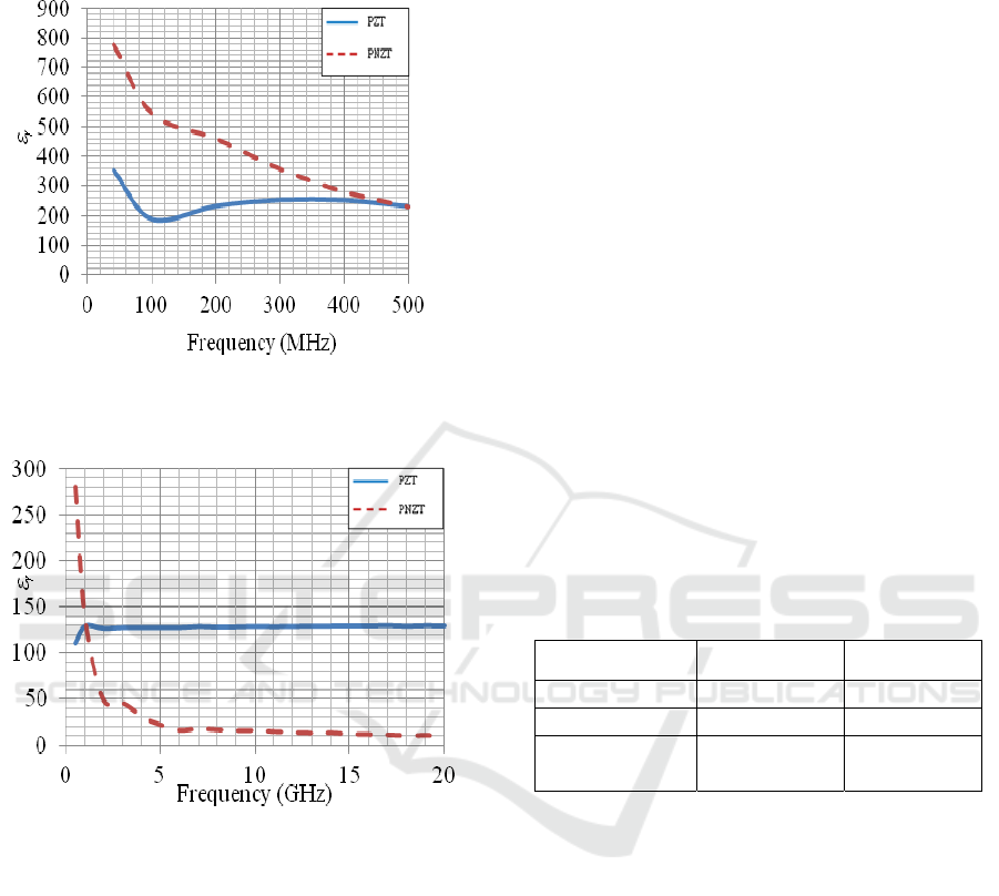
new results are repeated here. Figures 2 and 3 below
show typical response of the dielectric properties
over the frequency range mentioned. The PNZT
films exhibited higher permittivity compared to
PZT, this is expected due to the Nb doping. Both
films showed decreasing trends of ɛ
r
as the
frequency is increased, again this is expected as the
films get more lossy with frequency due to
polarization.
As expected, the decrease in ɛ
r
was accompanied
by an increase in loss tan for both samples
(Sulaiman et. al., 2011). The values of tan for the
PZT film were in the range of 0.04 to 0.18, while
similar behavior were seen for PNZT. This response
can be explained by the presence of the relaxation
phenomena where as the frequency of electric field
is increased, there is a point where the permanent
electric dipoles of the material can no longer rotate
fast enough to remain in phase with the field. Hence,
these mechanisms reduce the polarization and
PZT and Pnzt-Based Thin Film Capacitors and Transmission Lines for Microwave Integrated Circuit Applications
97
subsequently reduce the permittivity, while the loss
tangent increases (Al-Omari and Lear, 2005).
Figure 2: Permittivity versus frequency between 40 to 500
MHz.
Figure 3: Permittivity versus frequency between 0.5 to 20
GHz
From the results we could see the effect of
doping to PZT has significant impact on the
capacitor performance. Nb
5+
is a donor dopant which
replaces the Zr
4+
/Ti
4+
ions in the B-site of PZT - this
compensates the positive charge introduced
(Riemens et. al., 2003). Also, there is correlation
between the grain size and
r
with Nb concentration.
Riemens et. al, 2003, Haccart et. al. 2003 and Souza
et.al., 2004 reported enhancement to
r
with Nb
doping. However, the increase of
r
is also
influenced by composition as well as Nb
concentration. The work by Souza et.al 2004
showed that PNZT with high
r
has higher tan
ompared to PZT. Similar lossy behavior of PNZT in
our samples is seen in Figures 2 and 3.
The drastic decrease of
r
with frequency for
PNZT may be attributed to grain size as proposed by
(Chikuvula, 2000). The degradation of
r
can be
caused by several factors such as dielectric
relaxation and microstructure defects (Dimos and
Mueller, 1998; and Elisalde and Ravez, 2001). In
addition, different types of polarizations (which are
classified according to dipole type) can give rise to
several dispersion regions over the broad frequency
range. With the decreasing permittivity, therefore,
the loss is expected to increase with frequency. This
behavior was indeed observed for both our films
over the two frequency ranges. Many factors
contribute to dissipation in a ferroelectric material -
among them is the effect of oxygen and lead
vacancies (Park et. al., 2002; Chang and Anderson,
1997 and Zhu et. al., 2006), ferroelectric domain
wall motion, as well as film composition and
microstructure (Park, et. al., 2002; and Elissalde and
Ravez, 2001).
Table 1 summarizes the dielectric properties of
our films from 40 MHz to 20 GHz, and compares
with those of (Vilarinho, et. al., 2005). Though the
loss tangent in this work was higher, the permittivity
values were in the expected range for both thin
films.
Table 1: Comparison of material properties.
ɛ
r
tan д
PZT (this work) 110 - 353 0.04 – 0.1
PNZT (this work) 11 - 778 0.15 – 1.18
Vilarinho et. al.
2005
200- 1000 0.01 - 0.07
3.2 Transmission Lines
To demonstrate the feasibility of using these films in
MMIC, several transmission lines were constructed
on them. The lines were designed in both microstrip
and co-planar waveguide (CPW) form. The co-
planar waveguide format is preferred for high
frequency on-wafer probing due to the co-planar
arrangement of the Cascade probes used in this
work. The CPW is also preferred over microstrip in
MMIC applications since the former eliminates the
need to use via holes, which is difficult to realize,
and model, in MMIC. An example of the co-planar
waveguide line structure used in our work is shown
in Figure 4.
Second International Conference on Telecommunications and Remote Sensing
98
Figure 4: The test structure showing co-planar waveguide
transmission line fabricated on PNZT film.
3.2.1 Simulation Results
a) Effect of ɛ
r
The transmission lines were also simulated to predict
their behavior. The CST Microwave Studio
electromagnetic simulator was employed for this
purpose. In the simulation,
ε
r
values between 200 to
1000 were used to replicate the high-k properties of
the films. Figure 5 depicts the simulated insertion
loss values of CPW lines for different
ε
r
. The line
length and width were set to 100 µm and 5 µm
respectively. The CPW structure was treated as a
symmetrical configuration, (Kuang et. al., 2010;
Pozar, 2005 and Kitzawa and Itoh, 1991) with the
gap between the ground pad and the center
conductor set to 50 μm apart to comply with the
GSG probe pitch limitation. The tan value was
fixed to 1 as ceramic materials are normally lossy
(Pozar, 2005; and Mirshekar-Syahkal, 1983). The
results show that as
ε
r
increases; the insertion loss
increases with frequency. These results indicate that
for a given frequency; as the relative permittivity is
increased, the insertion loss is degraded. This is
because more rf energy is lost in the dielectric as
ε
r
is increased.
b) Effect of line geometry
The CPW was treated as symmetrical
configuration throughout the simulation. The gap s
was set to 50 μm to comply with the probe pitch,
while the centre strip line width w was varied.
However, the minimum w is limited by the
fabrication process. In this simulation the insertion
loss was computed when w was varied over two sets
of values - from 1 to 5 µm, and from 5 to 50 µm.
The results of these two sets of simulations are
shown in Figures 6 and 7 respectively.
ε
r
for both
simulations were set at 200, and the line length was
100 µm with loss tangent of 1. The electrode
thickness was fixed at 0.26 µm. The results in
Figures 6 and 7 illustrate that S
21
did not show a
significant dependency on the line width. Both sets
of results exhibit the same trend and comparable
insertion loss values.
Figure 5: Variation of insertion loss of CPW lines with
frequency for different
ε
r
values: 200 (), 400 (), 500
(), 600 (), 800 () and 1000 ().
Now, if the insertion losses are calculated with
different
ratios at a fixed frequency of 10 GHz, the response
obtained is shown in Figure 8 when w was varied
from 5 to 50 µm. It can be seen that the insertion
loss remain almost unchanged when w was varied.
Figure 6: Variation of insertion loss with frequency for
different line widths: 1 µm (), 2 µm (), 3 µm (), 4 µm
() and 5 µm ().
Frequency (GHz)
Insertion Loss (dB)
Insertion Loss (dB)
Frequency (GHz)
PZT and Pnzt-Based Thin Film Capacitors and Transmission Lines for Microwave Integrated Circuit Applications
99
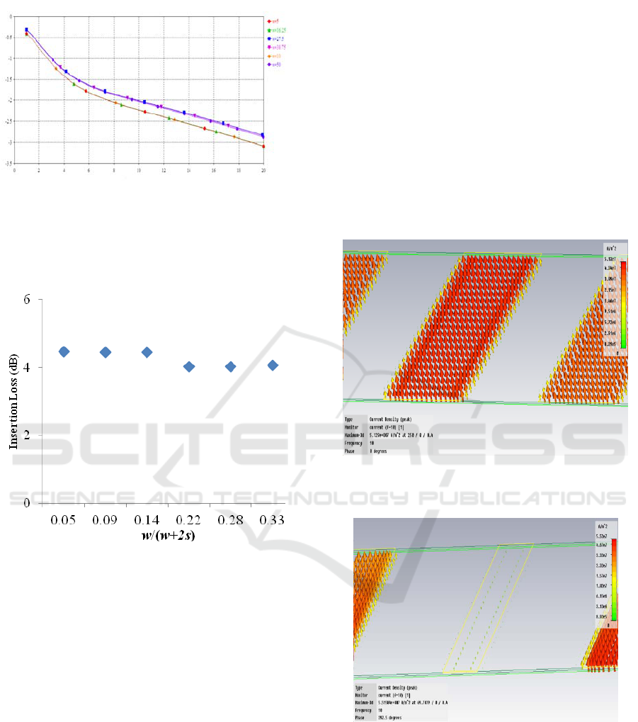
Figure 7: Variation of insertion loss with frequency for
different line widths: 5 µm (), 10 µm (), 16.25 µm (),
27.5 µm (), 38.75 µm () and 50 µm ().
Figure 8: Insertion loss versus w/w+2s for w = 5 to 50 µm
at 10 GHz.
Using the electromagnetic simulator the current
density distribution over the conducting strip was
examined. These are shown in Figures 9 and 10 for
cases where the width is decreased gradually from
50 µm to 16.25 µm. It can be seen that when the
width of the conducting strip is equal to those of the
ground planes the currents are equally distributed
(Figure 9), and as the width was reduced the current
density in the center conductor decreased as well –
this is expected since the line impedances are now
higher.
Current crowding at the conductor edges may
also affect the performance of a CPW besides
conductor surface roughness (Wen, 1969 and
Jackson, 1986). Using an electromagnetic simulator
this current can be examined quite conveniently as
shown in Figure 9. In this figure current crowding at
the conductor edge is revealed by plotting the
current density across the width of the conductor.
The current density values at the edge was about
5.13 × 10
7
A/m
2
, the arrows are more densely
located at the conductor edges, indicating current
crowding. As the metal thickness was set to be 0.26
μm, which is less than the skin depth of Au at 10
GHz (0.8 μm); this implies that the rf current flow is
concentrated at the edge of the lines in the slot
region. In contrast, when the width-gap ratio
decreases, as expected the current distribution in the
center conductor decreases too (Riaziat, 1990), as
shown in the plot of current density in Figure 10.
Figure 9: Current density of CPW for w = 50 µm.
Figure 10: Current density of CPW for w = 16.25 µm.
c) Effect of Film Thickness
As mentioned previously, the thicknesses of PZT
and PNZT films were 0.5 µm and 1.0 µm
respectively. In the simulation however, the film
thicknesses were varied to investigate the CPW
performance. The values of
ε
r
and tan
δ
were
obtained from the capacitance measurement: for
Frequency (GHz)
Insertion Loss (dB)
Second International Conference on Telecommunications and Remote Sensing
100
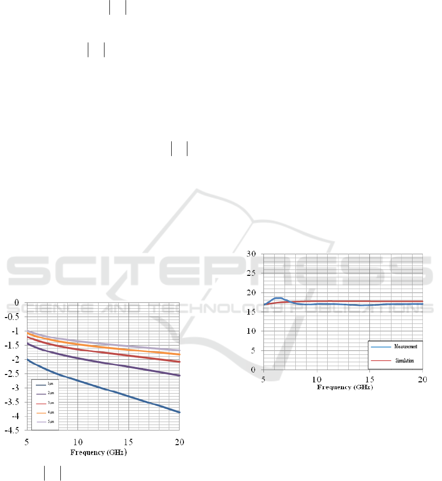
PZT they were 110 and 0.2, and for PNZT they were
280 and 1.
Figure11 shows the result of this simulation for
PNZT, where plots of
21
S
with PNZT film
thicknesses varying from 1 to 5 µm. Two things are
clear from the figure: firstly we see that the as the
film gets thicker,
21
S
decreases, implying a
reduction in the insertion loss. This behavior is
expected because as the film gets thicker, its
physical properties will be more uniform and
approach those of bulk samples. This is supported by
evidences reported in the literature (Zhi-Xiang et.
al., 2008, Haccart et. al., 2003 and Riemens et. al.,
2003) whereby bulk samples show better
performance than thin films. Secondly,
21
S
also
decreases with frequency, suggesting that the films
get more lossy with frequency. This is due to the fact
that at elevated frequencies the charges in the films
are unable to switch to the higher frequency electric
field. From the graphs it is important to note that for
practical integration circuit applications, it is
advisable not to use films thinner than 1 µm since
the losses degraded quickly after that. In this work,
the films used were 1 µm thick since it is quite
difficult to get thicker films using metal organic
deposition.
Figure 11:
21
S
versus frequency for PNZT films of
varying thicknesses.
3.2.2 Measurement Results
Test structures in the form of planar circuits such as
stripline, microstrip and co-planar waveguide are
commonly used for material property
characterization at microwave frequencies. These
test structures consist of dielectric substrates and
conductors that act as conducting strips and
grounding conductors. Microwave measurements are
made to examine the effect of substrate property and
conductor geometry so that microwave properties of
the circuit can be analyzed (Chen et. al. 2004).
In this work, experimental investigations of the
microwave behavior of both PZT and PNZT thin
films were performed using microstrip and co-planar
waveguide structures. In each structure, the PZT and
PNZT films which acted as a dielectric supported by
the silicon substrates.
The fabrication of the co-planar waveguide and
microstrip transmission lines was identical for both
films. The width and length of the lines are 5 μm
and 100 μm respectively. The structures were
measured with wafer probes in conjunction with a
vector network analyzer for high frequency
characterization. Measurement calibrations were
performed using the SOLT technique, aided by the
ISS impedance standard supplied by the probe
manufacturer. Two-port measurements were carried
out to evaluate the insertion loss of the films over a
frequency range of 5 GHz to 20 GHz.
Figure 12: Comparison of simulated and measured
insertion loss values of PNZT-based CPW.
Figure 12 shows the plot of one such result for
PNZT-based CPW, shown together with the
computer simulation for comparison. Both traces
show the same trend, and the agreement is quite
good, although the simulated values were slightly
higher. The results are the evidence that PNZT can
be used as a dielectric material in a CPW. The slight
discrepancies between the two results were probably
due to the mismatch loss that occurred in PNZT
films and to factors other than substrate properties –
this may include errors in the calibration and device
fabrication, and the electrode behaviour at high
Insertion Loss (dB)
PZT and Pnzt-Based Thin Film Capacitors and Transmission Lines for Microwave Integrated Circuit Applications
101
frequency. The mismatch happened due to the fact
the transmission lines were not exactly 50 – with
the high dielectric constants exhibited by the films,
the line width required to give 50 was too small to
be realized with our fabrication facilities. The
difference in the impedance of the line and that of
the probes would have given rise to reflections at the
input port, and this resulted in mismatch loss. In
addition, the loss of the PNZT-based CPW might not
only be due to the properties of the thin films
themselves, but to the geometrical aspects of the
transmission lines as well.
In the course of our work we found better
agreements with simulation were observed for
PNZT samples. We also found the PZT samples
exhibited higher insertion losses compared to PNZT
of the same line dimensions and film thickness.
PNZT-based CPW as a whole generally showed
better all round performance in our work.
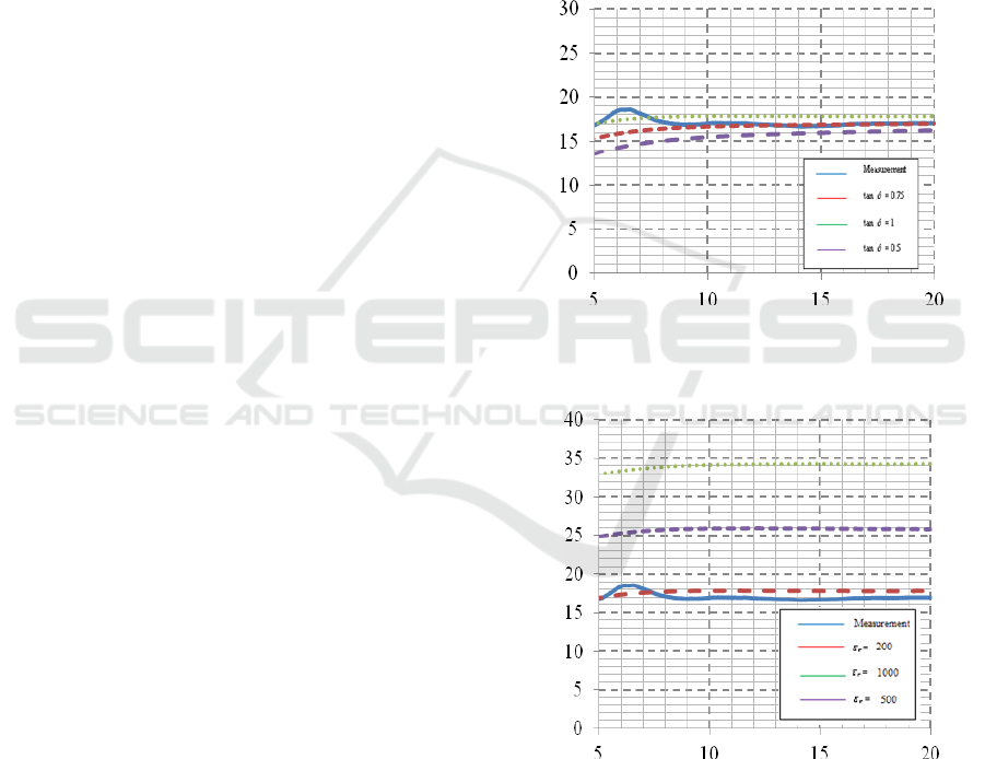
In order to determine the film properties, as well
as to investigate the effect of microwave frequency
on PNZT as a high-k material; a parametric study
was carried out by varying the film parameters, to fit
the simulation results with measurements. The line
dimensions were actual ones used in the fabrication,
while the film parameters such as ε
r
and tan
δ
were
varied. The effects of these variations on the
insertion loss are shown in Figures 13 and 14
respectively.
Figure 13 a) shows that as the loss tangent is
increased, the fit is better. This is expected from
theory since in a transmission line, the insertion loss
is mainly due to energy dissipation in the substrate
(in this case the ceramic film) – a material with high
loss tangent implies significant energy loss in the
material, and this leads to high insertion loss.
Ceramic materials in thin film form are known to be
quite lossy, and our results seem to concur with this.
In this example, a good fit between measurement
and simulation is obtained for ε
r
= 200 and tan
δ
= 1
as shown in Figures 13 a) and b) respectively.
Nevertheless our work has demonstrated that it is
possible to implement PNZT and PZT thin films for
use in MMIC.
4 CONCLUSIONS
PZT-based and PNZT-based thin film capacitors
have been fabricated and their performance
compared to investigate the effect of polarization at
high frequencies. The high frequency measurement
is divided into two frequency ranges; 40 MHz to
500
MHz and 500 MHz to 20 GHz. The results
reveal that Nb doping affect the relative permittivity
of the films, but the losses increased at high
frequencies. The relative permittivity values were
higher for PNZT films as expected due to doping.
The insertion loss characteristics of the films
were studied by implementing co-planar waveguide
transmission lines on PNZT. The films showed
acceptable performance and proved the feasibility of
using the films as a new substrate material for
microwave integrated circuits. Our future work will
include the use of these materials in the design of
passive MMIC devices such as filters and phase
shifters.
FREQUENCY (GHZ)
a)
FREQUENCY (GHZ)
b)
Figure 13: Comparison between simulated and measured
results of PNZT-based CPW transmission lines; with
adjusted a) tan
δ
and b) ε
r
.
INSERTION LOSS (DB)
I
NSERTION LOSS (DB)
Second International Conference on Telecommunications and Remote Sensing
102

ACKNOWLEDGEMENTS
The authors would like to thank Prof. Dr. Mohamad
Rusop and his team from the Nanotechnology
Research Group of University Technology MARA
for the assistance given in the fabrication. We are
also grateful to Dr. Sukreen Hana Herman for the
PZT thin film samples used in this work.
REFERENCES
Al-Omari A. N. and Lear K. L. 2005. Dielectric
Characteristics of Spin-Coated Dielectric Films using
On-wafer Parallel-Plate Capacitors at Microwave
Frequencies. IEEE Trans. on Electrical Insulation, 12,
1151-1161.
Bakar R. A. et. al. 2008. Optimized Fabrication Process of
PZT Thin Film Capacitor for MMIC Applications,
Proc. Int. Conf. on Nanosc. and Nanotech., Shah
Alam, Malaysia, Nov 18 – 21.
Chang L. H. and Anderson W. A. 1997. Single and
Multilayer Ferroelectric PZT on BaTiO
3
. Thin Solid
Films, 303, 94-100.
Chen L. F. et. al, 2004. Microwave Electronics:
Measurement and Material Characterization. New
York: John Wiley & Sons, Ltd., 382.
Chikuvula, V. et. al. 2000. Ferroelectric Dielectric for
Integrated Ciruit Applications at Microwave
Frequencies, US Patent 6146905.
Dimos D. and Mueller C. H., 1998. Perovskite Thin Films
for High-Frequency Capacitor Applications 1, Annual
Reviews in Materials Science, 28, 397-419.
Elissalde C. and Ravez J. 2001. Ferroelectric Ceramics:
Defects and Dielectric Relaxations”, J. of Mat. Chem.,
11, 1957-1967.
Haccart T. et. al, 2003. Substitution of Nb Doping on the
Structural, Microstructural and Electrical Properties
in PZT Films”, Thin Solid Films, 423, 235-242.
Jackson R. W. 1986. Considerations in the Use of
Coplanar Waveguide for Millimeter-Wave Integrated
Circuits, IEEE Trans. on Microwave Theory and Tech.,
34 (12), pp. 1450-
1456.
Kitzawa T. and Itoh T. 1991, Propagation Characteristics
of Coplanar Type Transmission Line with Lossy Media,
IEEE Trans. on Microwave Theory and Technique , 39
(10), 1694-1700.
Kuang, K. et. al. (eds). 2010. RF and Microwave
Microelectronics Packaging. Netherlands: Springer
Science + Business Media.
Mirshekar-Syahkal, D. 1983, An Accurate Determination
of Dielectric Loss Effect in Monolithic Microwave
Integrated Circuits Including Microstrip and Coupled
Microstrip Lines, IEEE Trans. on Microwave Theory
and Tech., 31(11), 950-953.
Park Y. et. al. 2002. Effect of Excess Pb on Fatigue
Properties of PZT Thin Films Prepared by Rf-
Magnetron Sputtering. Mat. Lett., 56, 481-285.
Pozar, D. M. 2005, Microwave Engineering, 3rd ed. New
York: John Wiley & Sons Inc.
Riaziat M. et. al,. 1990. Propagation Modes and
Dispersion Characteristics of Coplanar Waveguide,"
IEEE Trans. on Microwave Theory and Tech., 38 (3),
pp. 245-251.
Riemens D. et. al, 2003. Piezoelectric Properties of
Sputtered PZT Films: Influence of Structure,
Microstructure, Film Thickness (Zr,Ti) Ratio and Nb
Substitution, Materials Science in Semiconductor
Processing, 5, 123-127.
Setter N. et. al,. 2006. Ferroelectric Thin Films: Review of
Materials, Properties and Applications, J. App. Phys,
100, 510-606.
Souza, E. C. F. et.al. 2004. The Effect of Nb Doping on
Ferroelectric properties of PZT Thin Films Prepared
from Polymeric Precursors, Materials Chemistry and
Physics, 88, 155-159.
Sulaiman, S., Nadzar H. M. and Awang, Z. 2011,
Characterization of PZT and PNZT thin films for
monolithic microwave integrated circuit applications,
Proc. 2011 IEEE Region 10 Conf. (TENCON2011), pg.
1264 – 1268, Nov. 22 – 24, Bali, Indonesia.
Vilarinho, P. M. et al. (eds.). 2005. Scanning Probe
Microscopy: Characterization, Nanofabrication, and
Device Application of Functional Materials.
Netherlands: Kluwer Academic Publishers,
3-33.
Wen C. P. 1969. Coplanar Waveguide: A Surface Strip
Transmission Line Suitable for Non-reciprocal
Gyromagnetic Device Applications. IEEE Trans. on
Microwave Theory and Tech., 77 (12), pp. 1087-1090.
WinCal 3.2 User Guide. 2000, Cascade Microtech, Inc.
Zhi-Xiang et. al. 2008. Thickness and Nb-Doping Effects
on Ferro and Piezoelectric Properties Highly a-axis
Oriented Nb-doped Pb(Zr
0.3
Ti
0.7
)O
3
Films. J.of App.
Phys., 140, pp. 2003-2007, 2008.
Zhu C. et. al. 2006. The Effects of the PbO Content and
Seeding Layers upon the Microstructure and
Orientation of Sol-gel Derived PZT Films. J. Mat. Sc.:
Materials in Electronics, 17, 51-55.
PZT and Pnzt-Based Thin Film Capacitors and Transmission Lines for Microwave Integrated Circuit Applications
103
