Analysis of Photosensor Properties for Visual Neural Stimulators
Naser Pour Aryan and Albrecht Rothermel
Institute of Microelectronics, University of Ulm, Ulm, 89081, Germany
Keywords:
Dark Current, Epitaxy Process, Photodiode, Retinal Illuminance, Subretinal Chip.
Abstract:
Photodiodes are important elements in subretinal visual stimulation chips (Rao et al., 2006)(Rothermel et al.,
2009). This paper quantifies the advantages of using a process involving a low photodiode dark current per
unit area for fabricating these devices. Such a technology needs an epitaxy process to optimize the substrate
material lattice properties as also mentioned in (Cinguino et al., 1985) and (Inada et al., 2009). In the following
we show that the illumination on the retina is in a range that an epitaxy process ensuring low dark current
becomes beneficial. To the authors’ knowledge, this is the first study of its kind in open literature.
1 INTRODUCTION
Subretinal stimulator chips are among the devices giv-
ing rise to hope in curing blindness in people suffering
from Retinitis Pigmentosa (RP) or Age-related Mac-
ular Degeneration (AMD) (Rao et al., 2006)(Rother-
mel et al., 2009). Light sensing in these devices is
done through photodiodes. Among the important pa-
rameters in designing these photodiodes is the retinal
illuminance.
Retinal illuminance has been investigated before
(Mactier et al., )(Atchinson and Smith, 2000). Un-
fortunately these studies relate the retinal illuminance
to the luminance incident on the eye pupil. This ap-
proach has little significance in practice because pho-
todiode current is proportional to the illuminance (or
the irradiance) incident on the photodiode. Moreover,
compared to illuminance, devices used for luminance
measurement are much more expensive.
In the following we relate the retinal illuminance
to the illuminance incident on an object with a dis-
tance r from the eye. We assume that the object
is white and reflects all of the incident light. This
method enables us to apply the measured photosensor
voltage versus illumination characteristic to a retinal
chip and evaluate the interesting illuminance range.
Then, we show that regarding this range, photodiodes
fabricated in an epitaxy process which have a low
dark current per unit area are beneficial in subretinal
devices.
2 PHOTOSENSOR STRUCTURE
AND THE FABRICATED
DEVICE
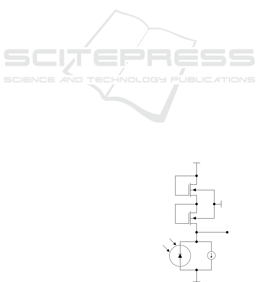
A photosensor circuit with a structure similar to the
one in (Rothermel et al., 2009) (Fig. 1) is fabricated
in CMOS technologies on bulk and epitaxy substrates.
Here V
dda
is equal to +2V and V
ss
is -2V. The current
source I
Photo
models the photodiode’s current induced
by the incident light and does not exist in the actual
structure. This current is linearly proportional to the
illuminance of the incident light. The two NMOS
V
dda
V
ss
V
ss
I
photo
MN0
Photosensor
output
MN1
D0
Incident light
Figure 1: The photosensor circuit fabricated and investi-
gated in this study.
40
Pour Aryan N. and Rothermel A..
Analysis of Photosensor Properties for Visual Neural Stimulators.
DOI: 10.5220/0004312400400044
In Proceedings of the International Conference on Photonics, Optics and Laser Technology (PHOTOPTICS-2013), pages 40-44
ISBN: 978-989-8565-44-0
Copyright
c
2013 SCITEPRESS (Science and Technology Publications, Lda.)
transistors MN0 and MN1 operate in the subthreshold
region, in which the MOSFETs exhibit an exponen-
tial current-voltage characteristic. So this structure
can be used to logarithmically compress a large range
of the photocurrent. Moreover, it has a logarithmic
response which mimics the photoreceptor’s behavior
in the human retina. For a MOS diode operating in
the subthreshold region, if the substrate effect is ig-
nored and it is assumed that its drain-source voltage
is much higher than the thermal voltage for simplicity,
the drain current I
D
is written as (Allen and Holberg,
1987):
I
D
=
W
L
· I
D0
e
V
GS
−V
th
nV
t
(1)
with
I
D0
∼
=
β
L
W
2(nV
t
)
2
e
2
(2)
Thus, the voltage drop on the diode V
GS
is
V
GS
= nV
t
ln(
I
D
L
I
D0
W
) +V
th
(3)
Here W is the gate width of the MOSFET, L the
gate length, n is the subthreshold slope factor which
is a process parameter with typically n = 1.14 → 1.5.
The thermal voltage V
t
is about 27mV at body temper-
ature. k is Boltzmann’s constant. T is device temper-
ature in Kelvins and q is the elementary charge value.
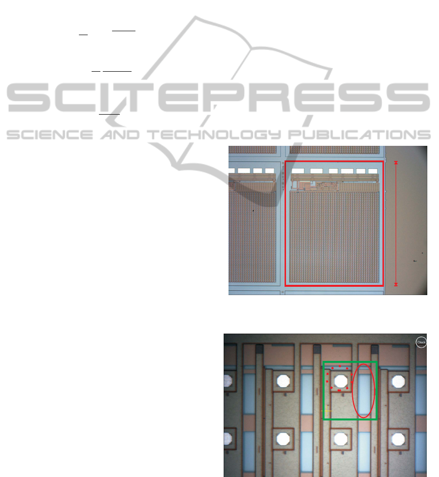
This photosensor circuit is fabricated together
with the rest of the stimulator chip in a silicon based
0.35µm CMOS process. A chip micrograph is illus-
trated in Fig. 2. The chip has 1600 pixels. A single
pixel is marked in Fig. 3 in the green rectangle. Ev-
ery pixel has an octagonal electrode with a diameter
of 15µm (in the dotted red circle) and a photodiode
with an area of 15µm x 48µm (in the red solid oval).
This chip is fabricated both in an epitaxy substrate
based process (Fig. 2) and a process without an epi-
taxy layer (not shown here, fabricated as a test-chip
with extra pads to measure the internal signals, in-
cluding the output voltage of the photosensor). The
thickness of the epitaxy substrate is 14µm.
In addition to the electrode and the photodiode
there are other amplifying and conversion circuitry in
the pixels which are not detailed further here.
3 MEASUREMENT RESULTS
The photosensors fabricated in the bulk and epitaxy
substrate based processes were measured indirectly.
The output electrode current of the pixel depends on
the photosensor voltage. By measuring this current,
photosensor voltage versus illuminance characteris-
tics in both processes were determined. The two pho-
tosensor characteristics are illustrated in Fig. 4. Be-
cause of measurement setup limitations, the illumi-
nance range was confined to 0.01 lux to 10 klux.
The test-chip with the bulk substrate provided the
voltage directly via a pad, so we could verify the in-
direct measurement method. The voltage of this pad
had to be measured with an op-amp (used as buffer)
having a very low input bias current, because the
photodiode current is very small in low illuminances
(1pA at 1 Lux). The option used here was LMC6044
from National Semiconductor, having an input bias
current of only 2 fA. The measured photosensor char-
acteristic was the same as in the indirect measure-
ment.
The illuminance was measured by a Minilux
luxmeter from Mx-electronic.
As is seen in Fig. 4, while the epitaxy process
based photosensor output remains linear over the
whole measurement range, the bulk based photosen-
sor saturates at lower illuminances. At low illumi-
3900 µm
Figure 2: The chip micrograph: A single chip is inside the
red rectangle.
Figure 3: Photo of a single pixel. The vertical and horizon-
tal pitch is 70µm.
AnalysisofPhotosensorPropertiesforVisualNeuralStimulators
41

nances, photodiode current drops below photodiode’s
dark current, so no sensitivity to illuminance is avail-
able any more.
We could determine the photodiode dark current
by comparing the measurement results with the sim-
ulations. For the epitaxy based process a dark cur-
rent of 600fA (corresponding to 0.83 nA/mm
2
) could
be determined. Note that a completely linear photo-
sensor characteristic does not mean a zero dark cur-
rent, because the MOSFETs have some leakage cur-
rent which compensates for the effect of photodiode
dark current. The transistor models used in the sim-
ulations take this into account. The bulk substrate
based process had a higher dark current: 2pA (cor-
responding to 2.77 nA/mm
2
).
4 RETINAL ILLUMINANCE
CALCULATION
In order to determine if an epitaxy process is benefi-
cial for a subretinal stimulator chip application, it is
necessary to calculate the retinal illuminance. This is
done in the following.
We consider the eye looking at an object illumi-
nated by an illuminance value I. We assume that the
object is 100% reflecting, is infinitesimally small but
has a definite area A (Fig. 5), thus it is practically a
point.
A corresponding image point with an area B
emerges on the retina. The luminous flux radiated
from the point into the whole right half-space is
I · A [lm]. The spatial angle spanning the half-space
is equal to 2πsr. So the luminous intensity into the
half-space (which is uniform because the point is very
small) is:
Intensity =
Flux
Angle
=
I · A
2πsr
(4)
0
0,1
0,2
0,3
0,4
0,5
0,6
0,7
0,8
0,9
0,01 0,1 1 10 100 1000 10000
Photosensor
outputvoltage
[V]
Illuminance[Lux]
Bulksubstrate
basedchip
Epitaxysubstrate
basedchip
Figure 4: The characteristics of the photosensor output volt-
age versus illuminance for bulk and epitaxy substrate based
chips.
r
A
Circular pupil
area
Eye
Illuminance=I
Figure 5: The eye looking at an infinitesimally small point
with an area of A.
The (luminous) flux into the eye is only the part of the
total flux radiating inside the angle α as in Fig. 5. So:
Flux into the eye[lm] = I · A ·
α
2πsr
(5)
So for the retinal illuminance:
Retinal illuminance[lux] = T · I ·
A
B
·
α
2πsr
(6)
T is the transmittance of ocular media and is on
the average 0.75 (Atchinson and Smith, 2000). Geo-
metric calculations give:
α
2πsr
=
Pupil area
Area o f a hemisphere with radius r
=
d
2
8r
2
(7)
Where d is the pupil diameter. The pupil diameter
range depends on the individual and age. The pupil
diameter is between 3 to 5mm when the environment
is bright. At the age of 15, the dark adapted pupil can
vary from 4mm to 9mm (Atchinson and Smith, 2000).
r is the object(point)-pupil distance.
We can approximate the transparent part of the
eye as a sphere having a constant refraction index of
n
0
∼
=
1.34, because the constituting material is simi-
lar every where (Meschede and Gerthsen, 2003) (see
Fig. 6). So the ratio of the point area to its image
on the retina can be calculated by the optical formula
corresponding to spherical transparent surfaces with
a refraction index different from 1. It depends on
the distance r, eye diameter a(image distance from
the cornea, where most of the refraction occurs, about
2cm) and n’ (Hering et al., 2007):
A
B
= (
n
0
n
)
2
· (
r
a
)
2
(8)
Here n is the air refraction index, which is
1. Mathematical calculations considering above as-
sumptions result in the following formula for retinal
illuminance at the point on the retina:
Retinal illuminance[lux] = T · I · n
02
·
d
2
8a
2
= 420.8m
−2
Id
2
(9)
PHOTOPTICS2013-InternationalConferenceonPhotonics,OpticsandLaserTechnology
42

Figure 6: The refraction index of different eye organs, from
(eye, http://hyperphysics.phy-astr.gsu.edu/).
A real white object which is uniformly illumi-
nated can be considered as a superposition of plenty
of points. The corresponding calculation should be
done through integration. The object is considered to
be large, i.e. its angular size is much larger than the
human eye angular resolution, which is 4 minutes of
arc. A good example is a uniformly lit white wall.
Therefore the effects of straylight (Vos et al., 1976)
and dullness of the retinal focus are canceled. The
resulting retinal illuminance is the same as above.
Therefore an object illuminance of 1 klux results
in a retinal illuminance of only 15.1 lux for d = 6mm.
This means that the retinal illuminance is about 2 or-
ders of magnitude lower than the illuminance of the
observed object. Table 1 lists the calculated retinal il-
luminance values for various conditions. From the ta-
ble we read a retinal illuminance range between 0.034
mlux to 736.4 lux.
5 DISCUSSION
As we see from Fig. 4, the bulk substrate based photo-
sensor enters saturation in retinal illumances between
1 and 10 lux. Table 1 shows that this is already prob-
lematic for vision in living room and in street light.
For retinal illuminances below 1 lux, the photosensor
output voltage is not sensitive to illuminance changes,
so no contrast (for example edges) can be perceived
any more. The epitaxy based photosensor remains to
be linear in darker environments. However, because
of measurement setup limitations, we were unable to
verify its functioning for illuminances lower than 0.01
lux. Anyway, the necessity of using epitaxy based
photodiodes with low dark current is revealed.
Table 1: The calculated retinal illuminance in different con-
ditions, the observed object is white and 100% reflective.
Situation Environment Retinal
Illuminance Illuminance
Sun, summer, 70 klux 736.4 lux
d=5mm
Cloudy day, 2 klux 30.3 lux
d=6mm
Well lit office 1 klux 15.1 lux
d=6mm
Living room 120 lux 2.47 lux
d=7mm
Street light 16 lux 0.43 lux
d=8mm
Full moon 0.25 lux 8.5 mlux
d=9mm
Stars but no moon, 0.001 lux 0.034 mlux
clear night, d=9mm
6 CONCLUSIONS
We have fabricated photosensors containing photodi-
odes with an area of 15µm x 48µm on both a bulk and
an epitaxy substrate based CMOS process. Our mea-
surements showed that while the epitaxy based pho-
tosensor is linear in the range of 0.01 to 10 klux, the
photosensor fabricated on bulk substrate loses linear-
ity below 10 lux and enters saturation around 1 lux.
We developed a mathematical method to calculate the
retinal illuminance using optics and anatomy knowl-
edge. By comparing these results and the measured
photosensor characteristics, we discovered the advan-
tage of an epitaxy based process for photodiode fab-
rication in subretinal neural stimulator devices.
ACKNOWLEDGEMENTS
The authors would like to thank Dr. Walter G. Wrobel
and Mr. Johannes Groeger for their support on this
work.
REFERENCES
http://hyperphysics.phy-astr.gsu.edu/.
Allen, P. E. and Holberg, D. R. (1987). CMOS Analog Cir-
cuit Design. Oxford University Press.
Atchinson, D. A. and Smith, G. (2000). Optics of the human
eye. Butterworth-Heinemann Ltd.
Cinguino, P., Genova, F., Rigo, C., and Stano, A. (1985).
Low dark current ingaas pin photodiodes grown
by molecular beam epitaxy. Electronics Letters,
21(4):139 –140.
AnalysisofPhotosensorPropertiesforVisualNeuralStimulators
43

Hering, E., Martin, R., and Stohrer, M. (2007). Physik f
¨
ur
Ingenieure. Springer-Lehrbuch. Springer.
Inada, H., Miura, K., Nagai, Y., Tsubokura, M., Moto, A.,
Iguchi, Y., and Kawamura, Y. (2009). Low dark cur-
rent swir photodiode with ingaas/gaassb type ii quan-
tum wells grown on inp substrate. In Indium Phos-
phide Related Materials, 2009. IPRM ’09. IEEE In-
ternational Conference on, pages 149 –152.
Mactier, H., Maroo, S., Bradnam, M., and Hamilton, R.
Meschede, D. and Gerthsen, C. (2003). Gerthsen Physik:.
Springer-Lehrbuch. Springer.
Rao, C., Yuan, X., Zhang, S., Meng, L., and Peng, C.
(2006). Cmos artificial subretinal chip for natural light
illumination. Electronics Letters, 42(15):849 – 850.
Rothermel, A., Liu, L., Aryan, N., Fischer, M., Wuen-
schmann, J., Kibbel, S., and Harscher, A. (2009). A
cmos chip with active pixel array and specific test fea-
tures for subretinal implantation. Solid-State Circuits,
IEEE Journal of, 44(1):290 –300.
Vos, J., Walraven, J., and Meeteren, A. V. (1976). Light
profiles of the foveal image of a point source. Vision
Research, 16(2):215 – 219.
PHOTOPTICS2013-InternationalConferenceonPhotonics,OpticsandLaserTechnology
44
