
AUTONOMOUS SENTINELS
FOR THE DETECTION OF INVASIVE PATHOGENS
Howard Clyde Wikle III, Suiqiong Li, Aleksandr Simonian and Bryan A. Chin
Materials Research & Education Center, Auburn University, Auburn, AL, U.S.A.
Keywords: Pathogen Detection, Biosensor, Bio-inspired, Phage, Magnetoelastic, Wireless Sensor.
Abstract: This paper describes the results of a research project to investigate and develop an autonomous pathogen
detection and capture system that mimics the function of naturally occurring biological defensive systems,
such as white blood cells. The autonomous sentinel system is envisioned to have the capability of seeking
out invasive pathogens in liquid environments, detecting and capturing them. Once detected and captured
the invasive pathogens can be removed, by retrieving the sentinels using a magnetic field. The sentinels are
composed of two main parts: a magnetoelastic resonator whose motion and detection functions is actuated
and monitored using magnetic fields; and a bio-probe that is immobilized onto the resonator surface and
captures specific target pathogens. The freestanding sentinels require no on-board power for motion or to
signal detection of a target pathogen. Upon contact with the target pathogen, the bio-molecular recognition
element on the sentinel will bind with the target cell. This will cause a mass change of the sentinel, which
results in a change in the sentinel's resonant frequency and the instantaneous detection of the target
pathogen. Similar to white blood cells, the autonomous sentinels when placed in a liquid analyte will move
through the analyte, capture and disable the target pathogens and signal their detection. The objective of
this paper is to demonstrate proof-in-principal of the concept of autonomous sentinels.
1 INTRODUCTION
For centuries, humankind has attempted to mimic
the designs of Nature to develop new engineering
materials and systems. The human blood system is
an excellent example of one of Nature’s amazing
creations that inspires us in this work. The human
blood contains many components that work
synergistically to keep us healthy. As part of the
immune system, white blood cells are the main
defensive mechanism against pathogenic invaders.
There are a variety of white blood cell types
(neutrophil, eosinophil, lymphocytes, etc.) that target
different pathogens. This capability serves as the
model for a bio-inspired system of autonomous
sentinels for the capture and detection of invasive
pathogens described in this paper (Figure 1). To
provide proof-in-principal of the concept, research
results for autonomous sentinel detection in liquid
analytes are presented in this paper. Potential short
term applications include the capture and detection
of bacteria in urine and liquid food products such as
water, juices and milk.
Figure 1: Bio-inspired sentinels will target different types
of bacteria (E. coli, Salmonella Typhimurium, etc.)
mimicking white blood cells that target different invasive
pathogens (Wetzel and Schaefer, 1982).
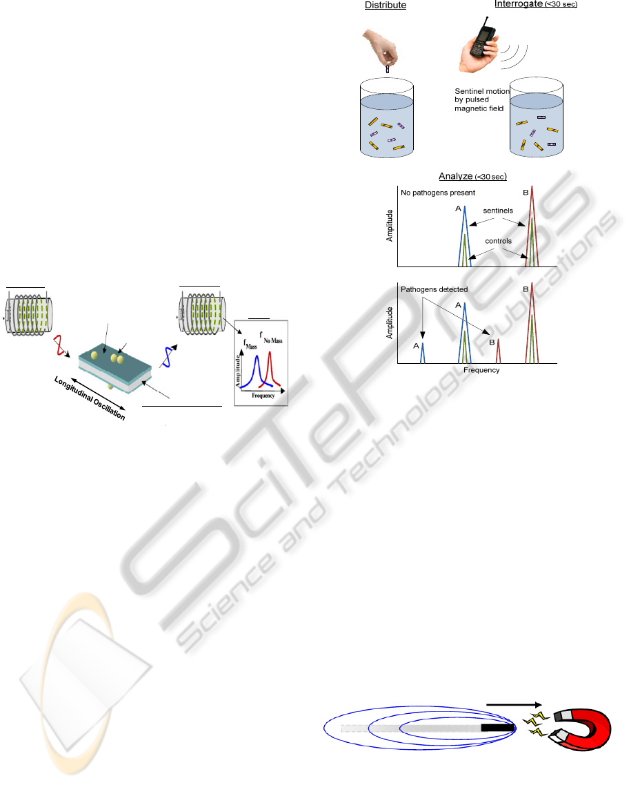
2 THEORY OF THE SENTINEL
A biosentinel is constructed of a freestanding
magnetoelastic (ME) resonator (transducer platform)
that is coated with a biorecognition layer
(bacteriophage) that specifically captures or binds a
single type of pathogen. The magnetoelastic
resonator investigated in the paper is strip-shaped, a
rectangular, flat piece of material. The resonator is
constructed from an iron-based, amorphous alloy
Nature
Bioinspired Sentinels
47
Wikle III H., Li S., Simonian A. and A. Chin B. (2012).
AUTONOMOUS SENTINELS FOR THE DETECTION OF INVASIVE PATHOGENS.
In Proceedings of the International Conference on Biomedical Electronics and Devices, pages 47-52
DOI: 10.5220/0003775200470052
Copyright
c
SciTePress
with magnetostrictive properties. Magnetostrictive
materials undergo a change in shape when subjected
to an applied magnetic field. If the magnetic field is
varied at the proper frequency aligned along the
length direction of the resonator, the structure can
achieve resonance. The detection principle of the
ME sentinels is shown in Figure 2. The freestanding
ME resonator serves as the transduction platform,
actuated into resonance by the application of an
alternating magnetic field. Upon contact with the
specific target bacteria, the bio-molecular
recognition element on the sentinel's surface
captures the target bacterial cells, causing the overall
sensor mass to increase which results in a decrease
in the resonant frequency. The resonant frequency is
remotely and wirelessly measured using a pick-up
coil. No onboard power is required by a sentinel.
Biorecognition Layer
Target
Pathogens
Apply Varying
Magnetic Field
ME Biosentinel
Resulting Field
Magnetoelastic Platform
nm to µm sized resonator
Result
Pick-Up Coil
Driving Coil
Figure 2: Detection principle of a magnetoelastic (ME)
biosentinel. A driving coil generates a modulated magnetic
field that drives the ME resonator into vibrational
resonance. Binding of the target bacteria to the bio-
molecular recognition layer immobilized onto the
resonator increases the mass of the sensor resulting in a
decrease in resonant frequency.
ME sentinels have unique advantages that stem
from both the magnetoelastic resonator platform and
the phage biorecognition layer. The sentinels are
wireless devices, enabling in-situ remote detection
of multiple target pathogens (Figure 3). Due to its
wireless nature, a large number of sentinels can be
deployed simultaneously, which significantly
enhances the probability of binding with a target
pathogen. More importantly, the binding of target
pathogens on only one out of many sentinels can be
easily detected. By taking advantage of these
properties and capabilities of phage-coated ME
resonators, a system of sentinels that mimics the
functions of white blood cells can be built and
deployed for enhanced medical diagnostics, food
safety, or water quality applications.
One of the key parameters of these Fe based, bio-
sentinels is the minimum detection limit. At low
bacterial concentrations, the odds of detection are
Figure 3: A large number of sentinels targeting different
pathogens may be mixed together and interrogated
simultaneously for pathogen detection. Different
pathogens may be detected simultaneously since the
sentinels for different pathogens are designed to operate in
different frequency ranges.
improved either by increasing the number of ME
sentinels deployed or by exposing the sentinels to a
dynamic environment. For detection in liquid media,
dynamic exposure can be achieved by flowing the
media past the immobilized sentinels or by moving
the sentinels around within the media. While flow
cells are a viable option, a simpler approach to
achieve greater exposure is to harness the magnetic
field that is currently used only for pathogen
detection to provide the forces for sentinel motion
(Figure 4). A nonuniform magnetic field can be used
to propel and steer the sentinels.
Figure 4: ME sentinel motion. A nonuniform magnetic
field generated by the detection system can be used to
induce movement in strip shaped sentinels.
BIODEVICES 2012 - International Conference on Biomedical Electronics and Devices
48

2.1 The Resonator Platform
Acoustic resonators as sensor platforms have been
widely investigated (Ballantine et al., 1997). Quartz
crystal microbalances, microcantilevers, surface
acoustic wave devices, and magnetoelastic particles
are all examples of acoustic resonators. Acoustic
resonators are mass sensitive devices where a
change in the mass load on the sensor surface causes
a change in the sensor’s resonant frequency.
Acoustic resonators are characterized by two
important parameters: 1) the sensitivity (S
m
) which
represents the shift in the initial resonant frequency
(Δf = f − f
0
) due to the attachment of a unit mass
load (Δm =m − m
0
) as shown in Equation 1 (Grimes
et al., 1999); and 2) the resonance performance (Q
factor), which is defined as the ratio of the energy
stored in the resonant structure to the total energy
losses per oscillation cycle. In an amplitude-
frequency spectrum, a measure of the Q factor is
given by the resonant frequency f divided by the 3
dB frequency bandwidth. A higher Q factor means a
sharper resonant peak and thus better resolution in
determining the resonant frequency. The minimum
detectable mass (
Δ
m
min
) for an acoustic sensor
platform depends on the ability to resolve resonant
frequency shifts as a result of the mass loading.
0
0
2
1
m
f
m
f
S
m
−≈
Δ
Δ
= (Δm << m
0
) (1)
For biological detection, the surface of the ME
sentinels is coated with a biorecognition element,
such as an antibody or phage. This biorecognition
element is designed to specifically bind the target of
interest. When the ME biosentinel comes into
contact with the target pathogens, the biorecognition
element will capture/bind the target pathogen
creating an additional mass load on the sentinel
resulting in a decrease in the resonant frequency.
Therefore, the presence and concentration of any
target pathogens can be identified by monitoring the
resonant frequency shifts of the sentinel. For a thin
strip-shaped ME resonator of length L, the largest
vibrations will occur along the length direction. The
fundamental resonant frequency of this longitudinal
oscillation is given as (Landau and Lifshitz, 1986,
Liang et al., 2007):
)1(2
1
0
υρ
−
=
E
L
f
(2)
where E, ρ, and υ are the Young’s modulus, density,
and Poisson ratio of the material respectively.
The sensitivity of the ME biosentinel is
compared with cantilevers in Figure 5. For ME
biosentinels and cantilevers fabricated from the
same material and of the same size, the ME sensor
exhibits an S
m
about 100 times better than the
cantilever. Advanced microfabrication processes
will enable the optimization of the resonance
performance of the ME sentinels which will lead to
improved pathogen detection capabilities. Different
shapes, structures, and/or material compositions are
parameters that affect sentinel motion, sensitivity
and resonance performance.
1x10
2
1x10
3
1x10
4
1x10
-6
1x10
-4
1x10
-2
1x10
0
1x10
2
1x10
4
Sensitivity (Hz/pg)
Len
g
th
(
um
)
Sentinels
Cantilevers
Figure 5: Sensitivity vs. length for cantilever and sentinels.
Sentinels are 100 times more sensitive.
2.2 Fabrication of ME Resonators
The ME resonators were fabricated using standard
microelectronic fabrication techniques of
photolithography and physical vapor deposition
(sputtering). The process used to fabricate the
resonators is shown schematically in Figure 6.
Binary alloy magnetoelastic resonators are
fabricated on a patterned wafer by co-depositing iron
and boron at controlled rates under vacuum. The
resonators are coated with gold that provides
oxidation protection for the alloy and a bioactive
surface to immobilize the phage. The resonators are
freed from the wafer by lift-off using an acetone
rinse and collected using a magnet. Fabrication of
the sensor platform begins by coating a 100 mm
plain silicon test wafer with a layer of chromium,
and then gold, each at a thickness of 30−40 nm. This
is accomplished using a Denton Vacuum Discovery-
18™ magnetron sputtering system, which employs
three cathodes (each holding a 3 inch diameter
target) aimed off-axis at a circular, rotating substrate
platform, along with DC and RF power supplies.
The gold layer is needed to adhere the next
deposited film (also gold) to the wafer, while the
AUTONOMOUS SENTINELS FOR THE DETECTION OF INVASIVE PATHOGENS
49
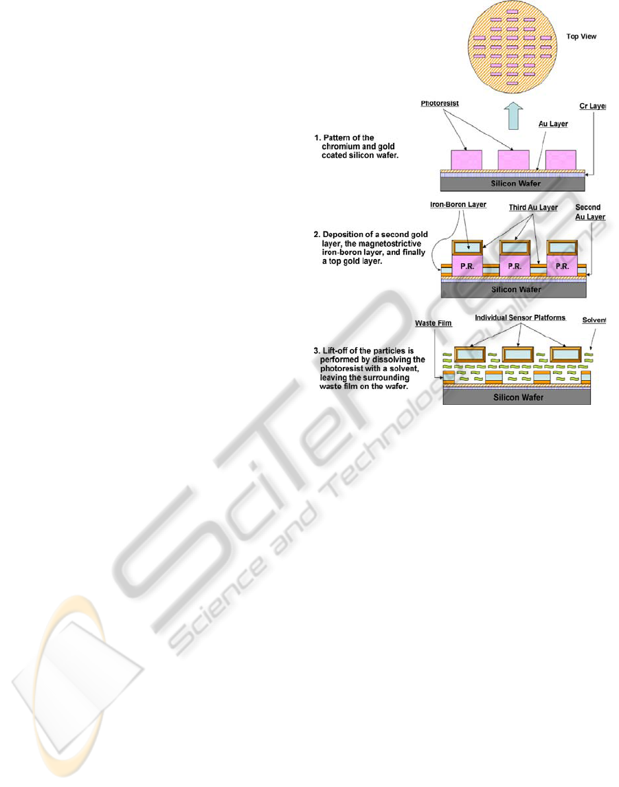
chromium merely serves to act as a bond between
the silicon and the gold. Next, a layer of photoresist
is applied to the gold surface of the wafer by spin
coating such that the resultant thickness is at least
twice that of the desired magnetoelastic film to be
deposited later. This photoresist is then UV exposed
using a positive mask comprised of evenly-spaced
rectangles, which are the desired length and width of
the magnetoelastic sentinels. The wafer is then
developed in a 2:1 solution of de-ionized water and
AZ-400K developer, rinsed, dried, and then
inspected for pattern integrity and thickness.
The magnetoelastic film is then deposited onto
the patterned wafer using the same sputtering system
as before. First, the wafer is loaded into the
deposition chamber, along with a gold, iron, and
boron target for each of the three cathodes, and then
the chamber is pumped down to 7×10
-7
Torr in order
to minimize residual oxygen in the film. Next, a gold
layer is deposited onto the patterned wafer to a
thickness of about 30–40 nm. The magnetoelastic
layer is formed by co-depositing iron (DC) and
boron (RF) simultaneously using a dual-cathode
method. This method differs somewhat from the
usual procedure for co-sputtering iron and boron,
which typically involves using a specially made
composite target. The advantage here is that the
power of each cathode can be tuned separately such
that the film has the desired composition at a
reasonable deposition rate. Thickness of this film
depends on process conditions, and is generally
limited by the thickness of the photoresist layer, but
highly magnetostrictive films of up to about 7 µm
have been obtained using this dual-cathode method.
Finally, another gold layer, using the same
processing conditions as before, is applied on top of
the iron-boron film, such that the magnetostrictive
particles will be completely enclosed in gold. From
an 8" wafer, approximately 40,000 sentinels can be
fabricated. The cost of fabrication of a single 8"
silicon wafer of sentinels is approximately $28.00.
Hence the cost of a single ME sensor is less than
1/1000 of a cent.
2.3 Immobilization of the
Bio-molecular Recognition Layer
To form functional sentinels, a bio-molecular
recognition element must be immobilized onto a
transducing platform to bind the specific target
pathogenic species. Other investigators typically use
traditional antibodies as the biorecognition element.
The strengths and weaknesses of antibody binding
are well known. An antibody is a relatively fragile
Figure 6: The ME resonator fabrication process.
species and subject to denaturation with
consequential loss of sensitivity and other binding
characteristics when exposed to unfavorable
environments. Moreover, the quality of antibodies
can vary with different animals and production
variables. To be used in sentinels, antibodies require
affinity purification and stabilization, which
dramatically increases their cost. Monoclonal
antibodies are more standard and selective, but their
application in the field is hindered by their stability.
The use of phage as substitute antibodies offers a
stable, reproducible and inexpensive alternative
(Petrenko, 2008, Petrenko and Smith, 2000). In
contrast to antibodies, the phage structure is
extraordinarily robust, being resistant to: heat (up to
80 °C) (Brigati and Petrenko, 2005); organic
solvents (e.g., acetonitrile) (Olofsson et al., 2001),
urea (up to 6 M), acid, alkali and other chemicals.
Purified phage can be stored indefinitely at moderate
temperatures without losing infectivity and probe-
binding activity. Three major factors contribute to
the high affinity binding of landscape phage to their
targets: a) constrained conformation of foreign
peptides; b) their multivalent display—thousands of
binding sites per phage filament; and c) extremely
high local concentration of binding sites. The
BIODEVICES 2012 - International Conference on Biomedical Electronics and Devices
50

surface area density of the phage is 300 to 400 m
2
/g,
exceeding even the best-known absorbents and
catalysts. The genetically engineered amino acids
that form the “active receptors” of a landscape phage
comprise up to 25% by weight of the phage and up
to 50% of its surface area—an extraordinarily high
fraction compared to natural proteins, including
antibodies.
Our research team has genetically engineered
filamentous phage (Figure 7), to serve as a
replacement for current antibody technology. The
filamentous E2 phage for binding to Salmonella
enterica serovar Typhimurium was affinity selected
from a landscape f8/8 phage library and provided by
the Department of Biological Sciences at Auburn
University (Petrenko and Sorokulova, 2004). The
clone E2 phage used in this work has been studied
and verified to be highly specific and selective
towards S. Typhimurium (Sorokulova et al., 2005).
The phage was immobilized on the ME sensor
surface using physical adsorption. Each ME sensor
platform was placed in a vial containing 300 μL of
phage E2 suspension (5×10
11
vir/mL in 1 x Tris-
Buffered Saline (TBS)). These vials were then
rotated and incubated on a rotor (running at 8 rpm)
for 1 hour. After the immobilization process, the
sensors were washed three times with 1 x TBS
solution and two times with sterile distilled water in
order to remove salt and any unbound or loosely
bound phage.
In order to reduce nonspecific binding, Bovine
Serum Albumin (BSA) solution was then
immobilized on the sensor surfaces to serve as a
blocking agent. The ME sentinels were immersed
into 1 mg/mL BSA solution for at least 1 hour,
followed by a distilled water rinse. In this study,
control sensors were fabricated and used to calibrate
the effects of environmental changes, such as
temperature and non-specific binding. The control
sensor is identical to the measurement biosensor
except it lacks the E2 phage coating. The control
sensors were also treated with BSA to block
nonspecific binding.
Major coat protein: pVIII
pVIpIII
pIXpVII
Major coat protein: pVIII
pVIpIII
pIXpVII
Figure 7: Filamentous Phage.
3 CHARACTERIZATION OF ME
SENTINEL PERFORMANCE
3.1 Detection of Pathogens by the ME
Sentinels
The S. Typhimurium culture (ATCC 13311) used in
this work was provided by the Department of
Biological Sciences at Auburn University, Auburn,
AL. These cultures were provided in the form of a
suspension at a concentration of 5×10
8
CFU/mL.
The suspensions were serially diluted in water to
prepare bacterial suspensions with the
concentrations ranging from 5×10
1
to 5×10
7
CFU/mL. All test solutions were prepared on the
same day as the biosentinel testing. The test
solutions were stored at 4 °C (during transfer and
storage) and equilibrated to room temperature in a
water bath prior to the experiments.
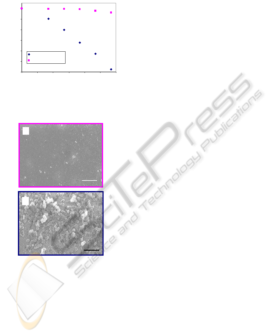
The resonant frequency of the sentinels was
measured using an HP 8751A network analyzer with
S-parameter test set. The ME sentinels (control and
measurement) were placed in a tube containing pure
water and the resonant frequency of the sentinel
measured. The network analyzer scanned, measured
and recorded the resonant frequency spectrum of the
ME sensor as a function of time. After each 30
minute exposure the analyte was changed to the next
highest dilution. Figure 8 shows the frequency shift
measurements for ME sentinels 500 × 100 × 4 µm in
size. Note that the control sensor shows a nearly
constant frequency (no frequency shift), while the
measurement sensor undergoes a frequency shift of
nearly 120,000 Hz. As can be seen from the plot, the
detection limit of the sentinel is better than 50
CFU/mL of S. Typhimurium in water.
A JEOL-7000F scanning electron microscope
(SEM) was used to confirm and compare the binding
of S. Typhimurium on the phage-coated
measurement and control sentinels. After the
detection, the ME sentinels were exposed to osmium
tetroxide (OsO
4
) vapour for 45 minutes. The sensors
were then mounted onto aluminum stubs and
examined using the SEM. Figure 9 shows the SEM
micrographs for the measurement and control
sentinels. The control sentinel shows only a few
cells are bound to the surface while the measurement
sentinel is nearly completely covered with bound S.
Typhimurium bacteria.
AUTONOMOUS SENTINELS FOR THE DETECTION OF INVASIVE PATHOGENS
51
-120000
-100000
-80000
-60000
-40000
-20000
0
1.E+00 1.E+01 1.E+02 1.E+03 1.E+04 1.E+05 1.E+06
Concentration of Salmonella Solution (CFU/ml)
Shift in the Resonance Frequency (Hz)
Measurement Sensor
Control Sensor
Figure 8: Response of 500 µm long biosensor exposed to
increasingly higher concentrations of S. Typhimurium.
The detection limit is less than 50 CFU/mL. The response
of the control sensor (devoid of phage) is also shown.
10µm
(a
10µm
(b
Figure 9: The SEM images show near zero binding of
Salmonella cells to the control sentinel (a) and a large
number of bound Salmonella cells to the measurement
sentinel (b).
4 CONCLUSIONS
Proof-in-principle of the concept of autonomous
sentinels for the detection of invasive pathogens has
been established. Magnetoelastic strip-shaped
resonators coated with a bio-molecular recognition
layer can moved through a liquid using a non-
uniform magnetic field and then measured remotely
and wirelessly to detect the binding and capture of
specific pathogenic bacteria. Because the
magnetoelastic sentinels investigated in this research
are iron based, they can be retrieved with a magnet
and hence captured pathogenic bacteria can be
removed from the system.
REFERENCES
Ballantine, D. S. Jr, White, R. M., Martin, S. J., Ricco, A.
J., Zellers, T., Frye, G. C., Wohltjen, H., 1997.
Acoustic wave sensors: Theory, design, & physio-
chemical applications, Academic Press. San Diego,
CA.
Brigati, J. R., Petrenko, V. A., 2005. Thermostability of
landscape phage probes. Analytical and Bioanalytical
Chemistry, 382, pp.1346-50.
Grimes, C. A., Stoyanov, P. G., Kouzoudis, D., Ong, K.
G., 1999. Remote query pressure measurement using
magnetoelastic sensors. Review of Scientific
Instruments, 70, pp.4711-14.
Landau, L. D., Lifshitz, E. M., 1986. Theory of elasticity,
Pergamon Press. Oxford, 3
rd
edition.
Liang, C., Morshed, S., Prorok, B. C., 2007. Correction
for longitudinal mode vibration in thin slender beams.
Applied Physics Letters, 90, pp.221912.
Olofsson, L., Ankarloo, J., Andersson, P. O., Nicholls, I.
A., 2001. Filamentous bacteriophage stability in non-
aqueous media. Chemistry & Biology, 8, pp.661-71.
Petrenko, V. A., 2008. Evolution of phage display: from
bioactive peptides to bioselective nanomaterials.
Expert Opinion on Drug Delivery, 5, pp.825-36.
Petrenko, V. A., Smith, G. P., 2000. Phages from
landscape libraries as substitute antibodies. Protein
Engineering, 13, pp.589-92.
Petrenko, V. A., Sorokulova, I. B., 2004. Detection of
biological threats. A challenge for directed molecular
evolution. Journal of Microbiological Methods, 58,
pp.147-68.
Sorokulova, I. B., Olsen, E. V., Chen, I. H., Fiebor, B.,
Barbaree, J. M., Vodyanoy, V. J., Chin, B. A.,
Petrenko, V. A., 2005. Landscape phage probes for
Salmonella typhimurium. Journal of Microbiological
Methods, 63, pp.55-72.
Wetzel, B., Schaefer, H., 1982. National Cancer Institute.
BIODEVICES 2012 - International Conference on Biomedical Electronics and Devices
52
