
A 130NM ASIC FOR EMG SIGNAL ACQUISITION
TO CONTROL A HAND PROSTHETIC
Lait Abu Saleh, Wjatscheslaw Galjan, Jakob Tomasik,
Dietmar Schroeder and Wolfgang H. Krautschneider
Institute of Nanoelectronics, Hamburg University of Technology, Eissendorfer Strasse 38, 21073, Hamburg, Germany
Keywords: EMG signal acquisition, Hand prosthetic, Bio-signal amplifier, Mixed-signal chip, Medical implant.
Abstract: A mixed-signal chip in 130nm Technology is described. The chip acquires EMG signals from five
differential inputs. The signals are amplified, multiplexed and digitized inside the developed chip. The
ASIC is optimised for low power and low noise and is intended for application in medical implants.
Furthermore, the chip provides a configuration options for several parameters for the analogue part of the
chip. The chip has been tested by recording EMG signals from implanted Myo-Electrodes.
1 INTRODUCTION
The loss of upper extremities puts several limitations
on trivial functions in daily life. The hand is
probably the most important part of the skeletal-
muscular system in the human body. Therefore
providing people with a proper alternative, which
replaces the lost functionality, constitutes an
important task. The purpose of the MyoPlant project
is the development of a bionic hand prosthesis
system with multiple degrees of freedom, based on a
myogenically controlled intelligent implant. The
project partners are the company Otto Bock
Healthcare GmbH, the German Primate Center DPZ
(Goettingen), the Fraunhofer Institut for Biomedical
Engineering (IBMT), the Technical University
Hamburg-Harburg and the Werner-Wicker-Clinic
(Bad Wildungen) and in cooperation with the
Medical University Vienna.
This article describes the development of an
application-specific integrated circuit (ASIC) for
invasive acquisition of muscular activity in order to
deliver an input for the controller of a hand
prosthetic. The ASIC is intended for use in the
implant above mentioned. The main task of the
ASIC is to record multiple EMG signals from
electrodes connected to the implant’s input, to
amplify the recorded signals, and to deliver these
signals digitally at the output. The digitized data
samples are collected by a microcontroller on the
implant, which sends them to a telemetry chip for
wireless transmission to the external system of the
hand prosthesis.
Volume, power consumption, low noise, and
efficiency play an essential role during the
development of an implantable system. A trade-off
between these parameters is often inevitable for the
developer. A transistor technology with small
feature size has many advantages considering area
reduction and power consumption. At the same time,
the same technology may have strong drawbacks in
terms of noise contribution and amplification factor.
2 SYSTEM REQUIREMENTS
AND SPECIFICATION
Muscle cells have a potential difference of ~100 mV
between the intra- and extracellular medium
(Principles of Neural Science, 2000), while
implanted electrodes record amplitudes in the range
of 100 μV – 5 mV. Therefore, a system for
amplifying these small bio-signals is needed. The
impedance of the used electrodes and the strength of
the bio-signal are important values for the
dimensioning of the bio-amplifier. The electrode
interface and the bio-amplifier input constitute two
impedances in series connected to the bio source
signal. This implies a voltage divider for the signal
source. The input impedance of the bio-amplifier
should be much larger than the impedance of the
electrode interface in order to obtain a large voltage
drop on the input of the amplifier.
The bio-amplifier also needs to accommodate the
149
Abu Saleh L., Galjan W., Tomasik J., Schroeder D. and H. Krautschneider W..
A 130NM ASIC FOR EMG SIGNAL ACQUISITION TO CONTROL A HAND PROSTHETIC.
DOI: 10.5220/0003765101490153
In Proceedings of the International Conference on Biomedical Electronics and Devices (BIODEVICES-2012), pages 149-153
ISBN: 978-989-8425-91-1
Copyright
c
2012 SCITEPRESS (Science and Technology Publications, Lda.)

voltage offsets of the electrode-tissue interface. In
order to overcome the problem of a comparatively
large DC offset on the differential input of the
amplifier, which might drive the amplifier into
saturation, an AC-coupling method was used for this
stage (R.R. Harrison, 2003).
The ASIC has an analogue to digital converter
(ADC) for digitizing the recorded signals. The
resolution of the ADC is set as a trade-off between
the target signal-to-noise ratio and the allowable data
rate by the telemetry chip. The use of an analogue
filter reduces the data rate while using a high
resolution at the ADC. Furthermore, the analogue
filter removes irrelevant signal frequencies by
limiting the bandwidth to the needed EMG-
bandwidth for controlling the prosthesis. A
configurable sampling rate at the ADC allows us to
change the data rate sent by the telemetry chip
according to link quality.
A well defined specification is very essential before
starting the development of an ASIC. The main
requirements of the developed ASIC can be
summarised as follows:
Low power consumption;
Low noise;
High common mode rejection ratio (CMRR);
Small silicon area;
Small data rate with high resolution.
Table 1: Specification of the ASIC.
Parameter Value unit comment
number of
channels
5
Input range
± 0.5
± 1
± 5
± 12
mV
Externally
configurable
Bandwidth
100 – 800
100 – 1500
Hz
Externally
configurable
Input
referred
noise
3
4
μV
rms
μV
rms
100 – 800 Hz
100 – 1500 Hz
CMRR 50 dB @ 50 Hz
Resolution 10 Bit
A supply voltage of 2.5 V – 3 V is needed for the
digital I/O-pads of the chip. The core voltage is
1.2 V (130 nm technology). This voltage must be
stable (voltage regulator with high Ripple Rejection)
in order to avoid fluctuations in the amplified signal.
Several methods for acquisition of bio-signals
(unipolar, bipolar or tripolar recordings) are reported
in literature. The chip was constructed for bipolar
acquisition method. The basic advantages of this
method are as follows:
Better symmetry in the input circuit;
Saves power on chip: No extra power for
amplification and distribution of the reference
potential to all amplifiers necessary;
No single point of failure (as in the case of
unipolar recording);
Surgically easier to perform;
Less vulnerable to interference from
neighbouring or from deep muscles.
On the other hand, this method needs more
electrodes and connected cables than the unipolar
method.
Figure 1: Chip architecture.
3 ARCHITECTURE AND DESIGN
A block diagram of the ASIC is shown in Fig. 1. It
has five analogue channels, which consist each of a
preamplifier and a low-pass filter. As a concept
study, the chip implements different circuit
alternatives in each channel. Channel 4 has a
multiplexer at the input in order to test the
functionality of switching between different
electrodes. The channels are combined by another
multiplexer, which directs the selected signal to a
programmable post-amplifier. An analogue to digital
converter (ADC) following the amplifier provides
the digitized signal at a 10-bit parallel port. A
configuration register with a serial interface is used
for setting the configuration parameters of the chip.
Further control lines are used to select the active
channel.
3.1 Analogue Front End
The analogue front-end consists of the preamplifiers,
low-pass filters, multiplexer, and post-amplifier.
BIODEVICES 2012 - International Conference on Biomedical Electronics and Devices
150
3.1.1 Preamplifier
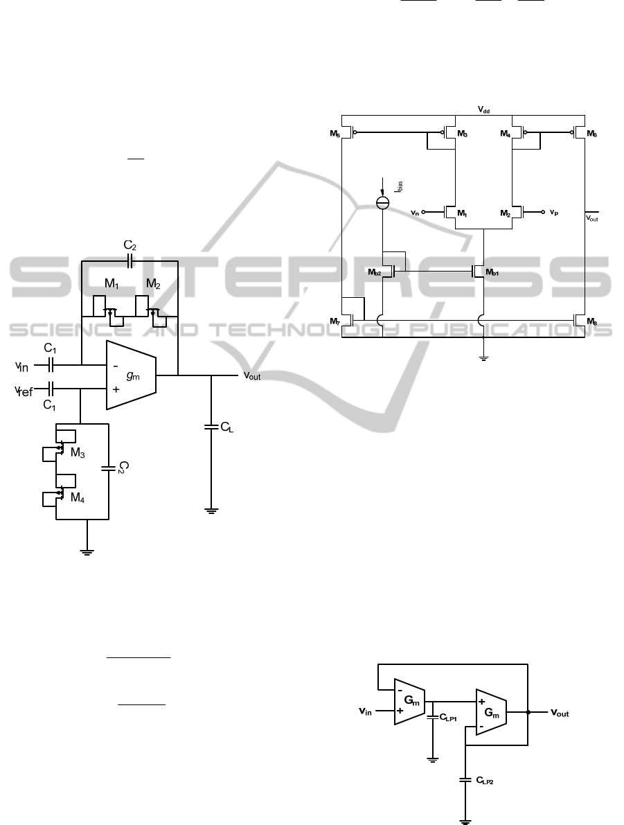
The preamplifier is shown in Fig. 2. It is based on
the proposal in Harrison 2003 and Harrison 2008,
which uses an operational transconductance
amplifier (OTA) as the amplification element. The
OTA delivers a current at the output that is
proportional to the differential voltage input. A
capacitive coupling by C1 and C2 determines the
voltage gain of the stage as
2
1
C
C
A=
(1)
The MOSFETs shown act as resistors (Harrison
2003), implementing very large resistances > 10
11
Ω
on a relatively small area.
Figure 2: Preamplifier.
The amplfier has a bandpass characteristic with the
corner frequencies:
,
2
1
2
CR
f
mos
L
π
=
(2)
AC
G
f
L
m
H
π
2
=
(3)
where R
MOS
denotes the resistance of the MOS-
resistors M
1
, M
2
and M
3
, M
4
mentioned above.
Fig. 3 depicts the circuit of the OTA. With
respect to the low-noise requirement, a high
transconductance of the input transistors is
advantageous in order to diminish the noise
contributions of the other transistors:
)21(
3
16
)(
1
7
1
3
1
2
m
m
m
m
m
n
g
g
g
g
g
kT
fv ++=
(4)
A triple well NMOS transistor was used at the input
stage of the OTA because it shows better noise
characteristics and better g
m
value than the PMOS
device.
Figure 3: Schematic of the OTA.
3.1.2 Analogue Low-Pass Filter
The low-pass filter suppresses unwanted frequencies
of the input signal (anti-aliasing). In order to obtain
an approximately brick-shaped transfer function and
to avoid large overshoot of the step response, we
implemented a Bessel low-pass filter (Tietze Schenk
2002), using the circuit shown in Fig. 4 (Geiger
1985).
A 5
th
order filter has been selected, which was
realised by the contribution of the preamplifier (see
above) and the series connection of two stages of
Fig. 4. This filter order represents a compromise
between sampling rate and analogue circuit
resources, since a higher filter order allows a lower
sampling rate and vice versa.
Figure 4: Second order low-pass filter.
A 130NM ASIC FOR EMG SIGNAL ACQUISITION TO CONTROL A HAND PROSTHETIC
151

3.1.3 Post-Amplifier
The task of the post-amplifier “PostAmp” (Tomasik,
2008) is further amplification of the signal and
driving the ADC input. Using an optimized setting
of its bias currents, an optimal trade-off between
low-power and low-noise operation can be
programmed (Tomasik, 2008).
3.2 Digital Part
The digital part of the chip consists of the analogue
to digital converter (ADC) and the configuration
register.
3.2.1 ADC
The ADC receives the signal voltage from the post-
amplifier and generates a 10-bit digital
representation at the output. A successive
approximation converter (SAR-ADC) has been
implemented. The most important advantages of this
architecture are low power consumption and small
chip area.
The SAR-ADC consists of a digital to analogue
converter (DAC), a comparator, and a digital control
circuit. The sampling rate has been chosen with
consideration to aliasing. The Nyquist condition
requests
samplesignal
ff
2
1
≤
(5)
The maximum power of unwanted signal fractions
has been specified such that the error is smaller than
½ LSB. Consequently, we obtain:
V
V
N
LSB
Err
2
1
2
1
2
1
11
==
(6)
dB
V
V
LSB
Err
66)(log20
10
−=
(7)
and the sampling frequency must be 2*f
-66dB
(see
Fig. 5) in order to satisfy the error specification and
to avoid aliasing effects. For the analogue channel
described here with its 5
th
order filter, the sampling
rate f
sample
becomes
kHzf
dB
2.10
66
=
−
(8)
kH
z
f
sample
4.20=
(9)
Figure 5: Frequency response of the analogue channel
3.2.2 Configuration Register
The configuration register is 40 bits long and stores
the parameters for the control of the chip. The
register is realised as a shift register that can be read
from or written to using a serial interface. The
configuration register controls the following
parameters:
• Signal bandwidth: The bandwidth of the
analogue channels can be selected between
(100-800 Hz) and (100-1500 Hz). It is defined
by a capacitor array in parallel with the load
capacitance of the preamplifier and a proper
selection of the bias currents of the filter OTAs.
• Channel 4: This channel has a multiplexer at its
input for higher reliability in case one electrode
pair at the input was defect. An electrode pair
with the lower impedance value will be selected
(external control).
• Power-Down: Each channel can be powered
down if necessary for reduced power
consumption.
4 EXPERIMENTAL RESULTS
The ASIC was fabricated in a 130-nm CMOS
process with a chip area of 1.525 mm x 1.525 mm
(Fig. 6).
Figure 6: The Myo-Chip on a match head.
BIODEVICES 2012 - International Conference on Biomedical Electronics and Devices
152
The measurement results are summarized in
Table 2.
Table 2: Measurement results.
Parameter Value Unit comment
number of
channels
5
Input range
± 0.5
± 1
± 5
± 12
mV
Externally
configurable
Channel gain
50
120
600
1200
Externally
configurable
Bandwidth
6 – 800
6 – 1500
Hz
Externally
configurable
Input referred
noise
2,2
2,5
μV
rms
μV
rms
6 – 800 Hz
6 – 1500 Hz
CMRR > 69 dB @ 50 Hz
Harmonic
Distortion
(without
ADC)
< 0.2 % @ 500 Hz
ENOB
(ADC)
8.5 Bit
Power
consumption
5.3 mW
For the whole chip
(incl. 5 channels)
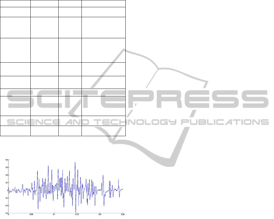
A measured EMG signal from the shoulder muscle
is depicted in figure 7.
time (sec)
A
m
plitu
d
e
(
m
V
)
Figure 7: EMG signal from the shoulder muscle.
5 CONCLUSIONS
An integrated circuit for the acquisition of muscle
signals (EMG) was presented. The chip is able to
amplify the recorded signals and to provide them
digitally at the output. It has an area of 1.525 x
1.525 mm
2
, consumes approx. 5.3 mW and can be
used in an implanted system. A future version of the
chip will contain an extended digital unit that
performs data compression and decimation of the
digital signals. Furthermore it implements a
communication protocol with a radio chip on an
implant to transmit EMG signals wirelessly from
inside the body.
ACKNOWLEDGEMENTS
Many thanks to all partners in this project for the
team spirit and the good collaboration. The project
MyoPlant was financed from the BMBF (Project
number: 16SV3699).
REFERENCES
H. Dietl, A. Gail, K.-P. Hoffmann, W. Krautschneider, T.
Meiners. Joint Project MyoPlant. BMT2010, Rostock,
Germany, 6.-8. Oct. 2010.
L. Abu-Saleh, W. Galjan, J. M. Tomasik, D. Schröder, W.
H. Krautschneider. An Implantable System for EMG
Signal Recording for controlling a Hand Prosthetesis.
BMT2010, Rostock, Germany, 6.-8. Oct. 2010.
J. Cardona Audi, C. Müller, O. Scholz, R. Ruff, K.-P.
Hoffmann. Real-time data link for wireless
implantable application. In 3
rd
European Conference
Technically Assisted Rehabilitation, TAR 2011,
Berlin, 17.-18. March 2011.
E. R. Kadell, J. H. Schwartz, T. M. Jessel. Principles Of
Neural Science. McGraw-Hill, Boston, MA, 2000.
R. R. Harrison, C. Charles. A Low-Power Low-Noise
CMOS Amplifier For Neural Recording Applications.
IEEE Journal Of Solid-State Curcuits, Vol. 38, No. 6,
pp. 958 – 965, 2003.
R. R. Harrison. The Design Of Integrated Circuits to
Observe Brain Activity. Proceedings of the IEEE, vol.
96, No. 7, pp. 1203 – 1216, 2008.
U. Tietze, Ch. Schenk. Semiconductor Circuit
Technology. 12. Edition, Springer, Berlin-Heidelberg,
2002.
R. L. Geiger, E. Sanchez-Sinencio. Active Filter Design
Using Operational Transconductance Amplifiers. A
Tutorial, IEEE Circuits and Devices Magazine, Vol. 1,
pp. 20-32, 1985.
J. M. Tomasik, K. M. Hafkemeyer, W. Galjan, D.
Schroeder, W. H. Krautschneider. A 130 nm CMOS
Programable Operational Amplifier. In Norchip 2008,
Tallinn, Estonia, 17.-18. Nov. 2008.
A 130NM ASIC FOR EMG SIGNAL ACQUISITION TO CONTROL A HAND PROSTHETIC
153
