
ANNEALING TEMPERATURE EFFECT ON THE SENSITIVITY
OF SIGE NANOWIRE FOR BIO-SENSOR
Kow-Ming Chang
1,2
, Chu-Feng Chen
1
, Yu-Bin Wang
1
, Chung-Hsien Liu
1
, Jiun-Ming Kuo
1
1
Institute of Electronics, National Chiao-Tung University, No. 1001, University Rd., Hsinchu 300, Taiwan, R.O.C.
2
Department of Electronic Engineering, I-Shou University, No. 1, Sec. 1, Syuecheng Rd., Kaohsiung, 840, Taiwan, R.O.C
Chiung-Hui Lai
Department of Microelectronics Engineering, Chung Hua University
No. 707, Sec.2, WuFu Rd., Hsinchu, 300, Taiwan, R.O.C
Keywords: Silicon nanowire, SiGe, Bio-sensor, 3-amino-propyltrime-thoxy-silane (APTS).
Abstract: Nanowire is widely used in biological sensor because it has the high surface-to-volume ratio. Germanium
(Ge) would be beneficial to enhance the sensitivity of silicon nanowire for bio-sensor. In this study, we have
successfully fabricated the
SiGe on Insulator (SGOI) nanowires with different annealing temperature by
side-wall spacer technique, respectively. The 3-amino-propyltrime-thoxy-silane (APTS) is used to modify
the surface, which can connect the bio-linker. Nanowire is considered as a resistance, and the change of
conductance (ΔG) and sensitivity (S) of different samples corresponding to APTS treatment were
investigated. As annealing temperature was elevated from 800 to 950℃, the SiGe nanowire exhibited
increasing sensitivity in the chemical detection. However, it was noted that degradation of sensitivity was
observed as the annealing temperature increases up to 1000℃. This behavior may be associated with the
reduction of the Ge concentration at the surface of SiGe nanowire due to high-temperature diffusion of Ge
in Si. So, temperature is a key parameter in the annealing process producing two effects: repairs of defects
and Ge diffusion. There would be an optimal annealing temperature between 900 and 1000℃.
1 INTRODUCTION
Silicon nanowire has recently attracted much
attention for its potential applications in the
biological and chemical sensors. Its sensing
mechanism is considered to be the change of its
electrical conductance upon surface as the bio-
molecular stay on it. Due to the large surface-to-
volume ratio and quasi-1D characteristics, the
silicon nanowire sensor provides a high sensitivity in
chemical detection such as PH buffer solution (Cui
et al., 2001), viruses (Patolsky et al., 2004), and
DNA (Li et al., 2004). Silicon nanowires are
particularly appealing for sensing applications, since
the silicon dioxide can effectively passivate surface
dangling bonds, and at the same time can be
chemically modified through the well known silanol
chemistry to provide surface functionalization and
selectivity for particular analytes.
Several studies have been attempted to fabricate
the nanowire by the advance photo-emission such
like Extreme Ultraviolet (EUV) or X-ray (Solak et
al., 1999), or the Atomic Force Microscope (AFM)
lithography (Nemutudi et al., 2001), or nanoimprint
(Yan et al., 2005), or sidewall spacer (Choi et al.,
2002), or vapor state synthesis (Mohanty et al.,
2007), or vapor-liquid-solid (VLS) growth (Li et al.,
2003). The sidewall spacer formation is an easy
process for nanowire fabrication with the advantages
of high-yield and low-cost. The method only using
the combination of the conventional lithography and
process technology was demonstrated without
complex processes such as electron beam
lithography (EBL), scanning probe lithography
(SPL) and VLS, etc.
It is reported that SiGe alloy has higher carrier
mobility than Si and can be thermally oxidized at
relatively low temperature. Moreover, SiGe field
345
Chang K., Chen C., Wang Y., Liu C., Kuo J. and Lai C..
ANNEALING TEMPERATURE EFFECT ON THE SENSITIVITY OF SIGE NANOWIRE FOR BIO-SENSOR.
DOI: 10.5220/0003153503450348
In Proceedings of the International Conference on Biomedical Electronics and Devices (BIODEVICES-2011), pages 345-348
ISBN: 978-989-8425-37-9
Copyright
c
2011 SCITEPRESS (Science and Technology Publications, Lda.)
effect transistor exhibits the higher current change as
the same gate voltage applied (Yeo et al., 2000). In
the previous works (Change et al., 2008a), it has
already demonstrated IgG antibody sensing
capability of SiGe nanowire sensor. First, the 3-
amino-propyltrime-thoxy-silane (APTS) was used to
modify the surface, which can connect the bio-linker.
APTS is used to modify the surface of native oxide
layer around nanowires. Hydroxyl functional groups
on the surface of native oxide layer were replaced by
the methoxy groups of APTS molecules. After
APTS modification, the surface of nanowire was
terminated by amine groups. In the experimental
environment, amine group is prone to be positively
charged, that is, the surface potential nanowire
increased, and the conductance of p-type nanowire
decreased. Next, bis-sulfo-succinimidyl suberate
(BS3) is used as linker between APTS and IgG
antibody. BS3 treatment resulted in negative charges.
Hence, the conductance of p-type nanowires
increased. After APTS and BS3 modification,
nanowire was capable of capturing IgG antibody.
Instead of the convention silicon nanowire, SiGe
nanowire sensor is expected to have better
sensitivity in the chemical detection for higher
carrier mobility as the same bio-molecular bind on
the surface. It is well known that annealing
temperature did repair the interior defects of SiGe.
The higher concentration of Ge the higher sensitivity
would become. However, excess of Ge will induce
more vacancies of surface, which will degrade the
adhesion between APTS and interface and decrease
sensitivity (Change et al., 2008b).
In this paper, we used the sidewall spacer
technique to fabricate the Si
0.93
Ge
0.07
and Si
0.86
Ge
0.14
nanowires with different annealing temperature for
discussion of the sensitivity, respectively. We focus
on investigating the change of conductance (ΔG) and
sensitivity (S) of different samples corresponding to
APTS treatment.
2 EXPERIMENT
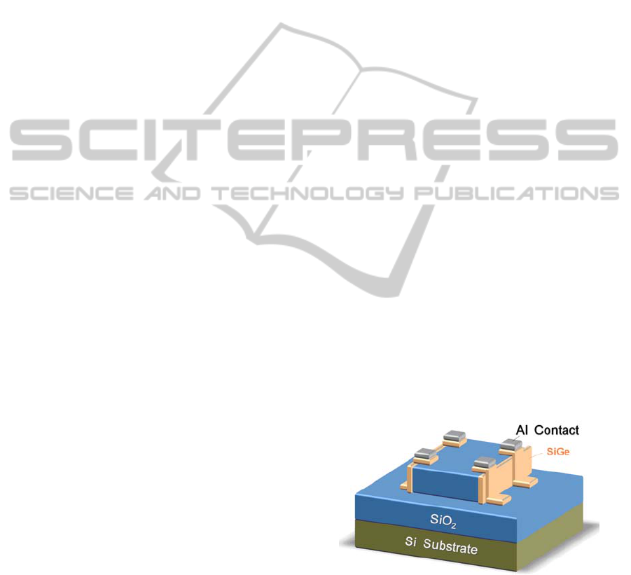
The structure is shown in Figure 1. All test samples
were fabricated on p-type (100)-oriented bare silicon
wafer with 1~10 Ω-cm resistivity. The poly-Si,
Si
0.93
Ge
0.07
and Si
0.86
Ge
0.14
nanowires were
fabricated by the side-wall spacer technique using
the combination of the conventional lithography and
processes technology, respectively. Starting with
standard RCA clean of silicon substrate, wet
oxidation was performed by SVCS Furnace system
at 980℃ for 7 hours to grow the bottom oxide of
about 5500 Å as an insulator oxide. After
lithography patterning of active area, oxide was
etched by Tokyo Electron Limited TE5000 Reactive
Ion Etch (RIE) system to form a 3000 Å oxide step.
Then, standard RCA clean was performed, followed
by a amorphous silicon (α-Si) film of 200 Å
deposition by SVCS Furnace system at 650℃ as
seed layer for SiGe film deposition. Then, a
polycrystalline SiGe film of 600 Å was deposited by
the ultra-high-vacuum chemical vapor deposition
(ANELAVA SiGe UHV-CVD) at 665℃. After
lithography patterning of the Source/Drain (S/D)
contact region, the SiGe film (800 Å, 20% over
etched) was etched by Transformer Coupled Plasma
(TCP) poly etcher. Only the S/D contact region and
the side-wall spacer retained SiGe. The residue SiGe
film is called SiGe nanowire. After lithography
patterning of removal of unwanted sidewall spacer,
the SiGe nanowire were etched and isolated. Finally,
Boron was heavily doped with 5×10
15
atoms/cm
2
at
10 keV to form p-type SiGe nanowire. Next, the
samples were subject to activation annealing in
nitrogen (N
2
) ambient at 800, 900, 950 and 1000 ℃
for 30 minutes. The aluminum was deposited by
thermal coater and patterned to reserve the S/D
region and sintered at 400
o
C for 30 minutes.
The Hewlett Packard HP 4156A was used in this
study to measure the electric characteristics of
nanowire sensor. Drain voltage (V
D
) was varied
from -10 to 10V and 500 mV a step, and back gate
voltage was 0 V. The measurement of electric
characteristics was performed ate every stage of
surface modification, and the average conductance
was then extracted from I
D
-V
D
characteristics with
V
D
= 3~6 V.
Figure 1: Schematic representation of SiGe nanowire
structure by the side-wall spacer technique.
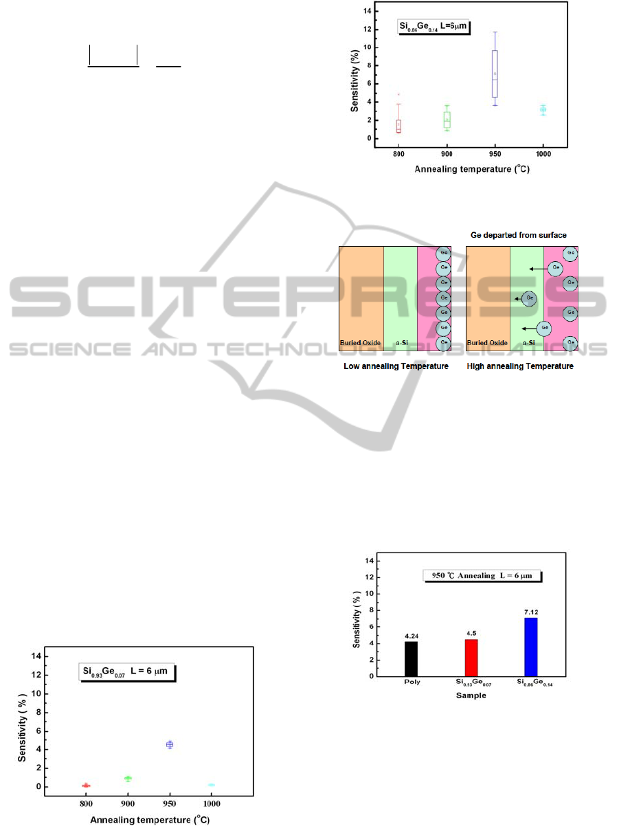
3 RESULTS AND DISCUSSIONS
The sensitivity (S) of a nanowire-based sensor is
BIODEVICES 2011 - International Conference on Biomedical Electronics and Devices
346
defined as the ratio of the magnitude of conductance
change to the baseline conductance value:
0
00
GG
G
S
GG
−
Δ
==
(1)
, where G
0
is the conductance before molecule
capture, G is the conductance after molecule capture,
and ΔG is the different between G and G
0
. Figures 2
and 3 show the sensitivity of the Si
0.93
Ge
0.07
and
Si
0.86
Ge
0.14
nanowire with different annealing
temperature after APTS modified, respectively.
Adequate Ge concentration will be more helpful to
enhance the sensitivity of silicon nanowire for bio-
sensor. The sensitivity increased slightly with
increasing annealing temperature from 800 to 900℃.
It is supposed that the annealing energy is
insufficient for repairing the defects. Furthermore, it
is observed that the raise of the sensitivity is more
obvious at temperature of 950℃ due to enough
energy to arrange. The sensitiveity of Si
0.86
Ge
0.14
nanowire could be 11.67% at 950℃ because of
better concentration and quality of Ge. However, it
is noted that a higher annealing temperature of about
1000 ℃ resulted in degraded sensitivity. This
behavior may be associated with reduction of Ge
concentration at the surface of SiGe nanowire
because the velocity of Ge diffusion toward Si
would be increased at higher temperature (Sugiyama
et al., 2004). Figure 4 is a schematic of the Ge
diffusion at low and high temperatures. So,
temperature is a key parameter in the annealing
process producing two effects: repairs of defects and
Ge diffusion. There would be an optimal annealing
temperature between 900 and 1000℃.
Figure 5 shows the sensitivity of poly-Si, Si
0.93
Ge
0.07
and Si
0.86
Ge
0.14
nanowire with annealing temperature
of 950℃ after APTS modified. The higher
concentration of Ge exhibits the higher sensitivity.
Figure 2: Sensitivity of Si
0.93
Ge
0.07
nanowire with different
annealing temperature after APTS modified.
Figure 3: Sensitivity of Si
0.86
Ge
0.14
nanowire with different
annealing temperature after APTS modified.
Figure 4: Schematic illustration of Ge diffusion at low and
high temperatures.
From the above, we conjecture that nanowire
obtains more energy at 950℃ to arrange the lattices
more regularly. Therefore, the lower defects make
the higher sensitivity increase. Hence, there would
be an optimal annealing temperature of about 950℃
in order to obtain better quality and higher
sensitivity.
Figure 5: S Sensitivity of poly-Si, Si
0.93
Ge
0.07
and
Si
0.86
Ge
0.14
nanowire with annealing temperature of
950℃after APTS modified. The higher concentration of
Ge becomes the higher sensitivity.
4 CONCLUSIONS
In this paper, we have investigated the effect of
ANNEALING TEMPERATURE EFFECT ON THE SENSITIVITY OF SIGE NANOWIRE FOR BIO-SENSOR
347

different annealing temperature on the sensitivity of
SiGe nanowire with Ge 7% and 11%. Raising the
annealing temperature can bring large sensitivity due
to repairs of defects, but it will degraded sensitivity
due to Ge diffusion as the annealing temperature
increases up to 1000℃. There would be a reasonable
annealing temperature between 900℃ and 1000℃.
It is concluded from experiments that the optimized
annealing temperature is around 950℃. Adequate
Ge concentration will be more helpful to enhance
the sensitivity of silicon nanowire for bio-sensor.
Si
0.86
Ge
0.14
nanowire with annealing temperature of
about 950℃ can obtain higher sensitivity (~11.67%)
in the APTS detection.
ACKNOWLEDGEMENTS
The authors would like to thank the staff of the
National Nano Device Laboratory for their technical
help. They also acknowledge the financial support of
the National Science Council (NSC) under Contract
Nos. NSC 98-2221-E-009-174-MY3.
REFERENCES
Cui, Y. (2001). Nanowire Nanosensors for Highly
Sensitive and Selective Detection of Biological and
Chemical Species. Science, 293, 1289-1292.
Li, Z. (2004). Sequence-Specific Label-Free DNA Sensors
Based on Silicon Nanowires. Nano Letters, 4(2), 245-
247.
Patolsky, F. (2003). Electrical detection of single viruses.
Proc. Natl. Acad. Sci. U.S.A., 101, 14017- 14022.
Solak, H. H. (1999). Exposure of 38 nm period grating
patterns with extreme ultraviolet interferometric
lithography. Appl. Phys. Lett., 75(15), 2328-2330.
Nemutudi, R. (2001). Modification of a shallow 2DEG by
AFM lithography. Microelectronic Engineering, 57,
967-973.
Yan, X. M. (2005). Fabrication of large number density
platinum nanowire arrays by size reduction
lithography and nanoimprint lithography. Nano Letters,
5(4), 745-748.
Choi, Y. K. (2002). A Spacer Patterning Technology for
Nanoscale CMOS. IEET Transactions on Electron
Devices, 49(3), 436-441.
Mohanty, P. (2007). Simple vapor-phase synthesis of
single-crystalline Ag nanowires and single-nanowire
surface-enhanced Raman scattering. J. AM. CHEM.
SOC., 129, 9576-9577.
Li, C. (2003). Diameter-controlled growth of single-
crystalline In
2
O
3
nanowires and their electronic
properties. Adv. Mater., 15(2), 143-146.
Yeo, Y.-C. (2000). Enhance Performance in Sub-100 nm
CMOSFETs using Strained Epitaxial Silicon-
Germanium. IEDM, 00-753.
Change, K.-M. (2008a). The Ge enhance the sensitivity for
bio-sensor. 2
nd
IEEE International Nanoelectronics
Conference, 811- 814.
Chang, K.-M. (2008b). Higher drive current for SiGe
nanowires. 2
nd
IEEE International Nanoelectronics
Conference, 315-319.
Sugiyama, N. (2004). Temperature effects on Ge
condensation by thermal oxidation of SiGe-on-
insulator structures. Journal of Applied Physics, 95(2),
4007-4011.
BIODEVICES 2011 - International Conference on Biomedical Electronics and Devices
348
