
CATECHOL DETETION USING AN OPTICAL MEMS SENSOR
Peter H. Dykstra, Stephan T. Koev, Reza Ghodssi
MEMS Sensors and Actuators Lab, Department of Electrical and Computer Engineering
Institute for Systems Research (ISR), University of Maryland, College Park, MD 20742, U.S.A.
Gregory F. Payne
University of Maryland Biotechnology Institute (UMBI), Rockville, MD 20850, U.S.A.
Liangli Yu
Department of Nutrition and Food Science, University of Maryland, College Park, MD 20742, U.S.A.
Keywords: Catechol, Chitosan, Waveguides, Absorbance.
Abstract: We report the successful fabrication and testing of an optical MEMS sensor for the detection of the toxic
phenol, catechol. Catechol’s presence in food and drinking water posses a health concern due to its harmful
effects on cell respiration. By-products of catechol oxidation have demonstrated increased absorbance
changes in a chitosan film in the UV and near UV range. Our reported sensor takes advantage of this unique
absorbance property to detect catechol by measuring the change in light intensity at 472 nm, thus
eliminating non-specific responses that occur from other oxidized chemicals which do not cause the
absorbance change. Concentrations as low as 1 mM catechol are detected while control experiments
including ascorbic acid display no measurable response.
1 INTRODUCTION
Monitoring the safety of our water supply by using
portable, efficient and inexpensive devices has
become an area of growing interest over the past
decade. The growth of industry has contributed to
the contamination of ground waters with various
potentially dangerous organic chemicals. Catechol is
a synthetic phenol commonly generated in factory
processes and it has been proven to have detrimental
health effects (Starek, 2003). One monitoring
solution is through the use of
microelectromechanical systems (MEMS) to create
on-chip sensors which can give field personnel
accurate and sensitive data on-site regarding the
testing of the water supply.
Recently reported sensors for catechol detection
either use optical or electrochemical measurement
schemes. Optical sensors making use of absorbance
(Abdullah et al., 2006) and fluorescence (Wu et al.,
2004) detection have been reported but the necessity
for bulky, external measuring equipment has
hindered the fabrication of such devices on chip.
Electrochemical sensors typically employ a standard
three electrode system with the working electrode
covered by an immobilization matrix such as
calcium carbonate to entrap oxidizing enzymes
(Shan et al., 2007). Although these devices result in
high sensitivity, the enzyme activity degrades over
time and can be directly affected by certain
conditions such as the pH of the solution making
these sensors difficult to calibrate.
Our reported device utilizes an optical
absorbance technique in a sealed microfluidic
channel for the detection of catechol. In order to
amplify the effect of the detected absorbance by
catechol oxidation, the aminopolysaccharide
chitosan is deposited in the microfluidic channel,
thus intersecting the pathway of the light through the
device. The proposed detection scheme does not
require the use of enzymes yet still remains selective
to phenolic compounds vs other chemical agents.
104
Dykstra P., Koev S., Ghodssi R., Payne G. and Yu L. (2009).
CATECHOL DETETION USING AN OPTICAL MEMS SENSOR.
In Proceedings of the International Conference on Biomedical Electronics and Devices, pages 104-108
DOI: 10.5220/0001552001040108
Copyright
c
SciTePress
2 MATERIALS AND THEORY
2.1 Catechol
Catechol is a benzenediol, which is a subset of the
phenol class of organic compounds. The chemical
formula of Catechol is C
6
H
4
(OH)
2
.
Following
oxidation, catechol loses its hydrogen atoms from
the hydroxyl groups and becomes an
orthobenzoquinone, more commonly referred to as
an o-quinone. The oxidation of catechol in the cell
creates free radicals which cause damage to vital cell
components such as lipids, proteins and DNA (Sies,
1997).
2.2 Chitosan
Chitosan is a unique material that is well suited for
biological micro-devices due to its ability to be
selectivity deposited and its high density of amine
groups, which provide active bonding sites. The
selective deposition occurs due to chitosan’s
insolubility above a pH of 6.5. At low pH, chitosan
is protonated and soluble in water. As the pH rises
above 6.5, the amines lose their net positive charge
and the chitosan becomes insoluble. By taking
advantage of this property, one can deposit a film of
chitosan onto a cathode during an electrochemical
reaction. The pH rises with increasing proximity to
the cathode due to the reduction of the hydrogen
ions. The chitosan forms as a thin film or hydrogel
over the cathode surface depending on the amplitude
of the applied current density.
Chitosan has an added advantage over other
polysaccharides because it contains nucleophilic
primary amine (NH
2
) groups at nearly every
repeating sugar residue in its structure. The o-
quinones, which are formed from the oxidized
catechol molecules, bind to the amine groups and
impart physical changes to the film, such as a
change in the optical absorbance (Wu et al., 2005).
2.3 Optics
Understanding the operating principle of the device
requires a more detailed understanding of light
propagation and absorption through a medium. The
absorbance can be related to the concentration of
absorbing species present as demonstrated by the
Beer-Lambert Law:
lc
I
I
A
ε
=−= )(log
0
1
10
(1)
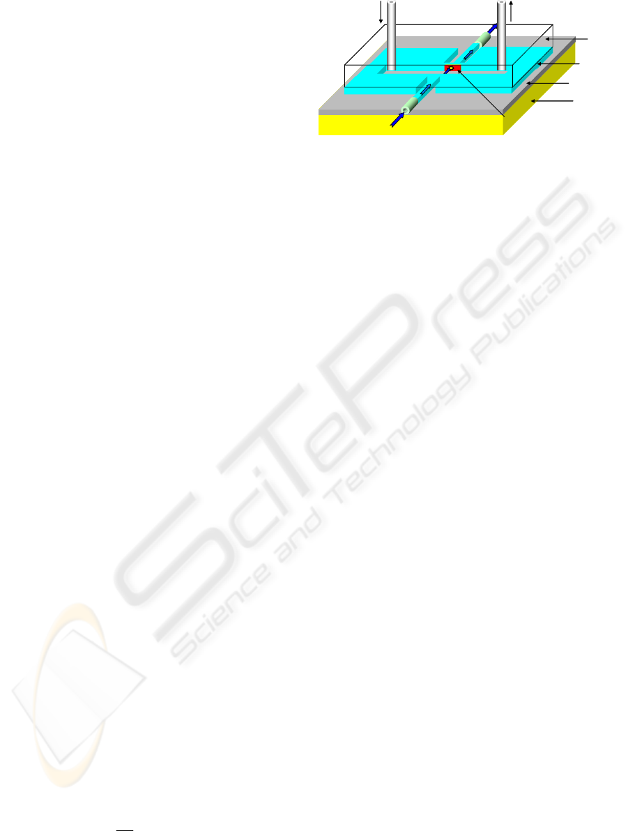
Fluid In
Fluid Out
Light In
Light Out
SU-8
Oxide
Deposited Chitosan Film
Silicon
PDMS
Fluid In
Fluid Out
Light In
Light Out
SU-8
Oxide
Deposited Chitosan Film
Silicon
PDMS
Figure 1: 3-d Schematic of the packaged device. The
device dimensions are 3.2 x 2.4 x 0.24 cm.
Where ε is the molar absorptivity, l is the path length
the light takes as it propagates through the absorbing
layer and c is the concentration. In our experiments,
the path length, l, is defined as the thickness of the
deposited chitosan film. O-quinones have been
reported to show a strong absorbance in the UV and
near UV range of the electromagnetic spectrum (Wu
et al., 2005). For this reason, a blue laser source at
472 nm was chosen for the optical measurements
taken with the MEMS sensor.
In our device, on-chip waveguides are patterned
from the polymer SU-8 as shown in the device
schematic (Figure 1). Blue light is coupled in and
out of the waveguides via multimode fibers with a
core diameter of 62.5 μm. The cross sectional area
of the polymer waveguides is 100 μm by 150 μm.
The light propagates through a film of chitosan that
has been deposited onto a transparent, conductive
film of indium tin oxide.
Since the absorbance measurement is purely
related to the optical power being received, it is
important to understand the different optical loss
mechanisms through the device in order to achieve
an acceptable signal to noise ratio. The primary
sources of loss are caused by waveguide losses
which include material absorption and scattering,
divergence of the light crossing the channel, and
roughness associated with the waveguide facets.
Waveguide loss will occur due to the roughness
of the waveguide and any material absorption
through the SU-8. This attenuation was measured to
be 21.15 dB/cm at 472 nm for waveguides with our
dimensions using image processing software. A top-
down digital photograph was taken of fabricated test
waveguides coupled to a blue laser source. The light
intensity down the length of the waveguide was
analyzed to determine the attenuation coefficient.
Divergence of the light as it crosses the
microfluidic channel from one waveguide to the next
is another possible source of loss. The light
capturing efficiency from one waveguide to the next
is found by integrating the surface energy of a beam
CATECHOL DETETION USING AN OPTICAL MEMS SENSOR
105
with a Gaussian profile and is related to the width of
the beam waist as seen in (2).
2
0
2
0
)(
*)(2
wzw
wzw
+
=
η
(2)
Where w
0
and w(z) are the width of the beam
waist before and after it has traversed the channel.
For the dimensions used in our device, the coupling
efficiency of the light as it traverses the channel
from one waveguide to another is near unity (η =
0.99). The high coupling efficiency is a result of
using waveguides with large cross sectional areas.
With these considerations, the most significant
factor that contributes to optical loss in the device is
the roughness of the waveguide facets and sides. The
surface roughness of the waveguides is an inherent
limitation when using lithography and cannot be
completely avoided.
3 DEVICE FABRICATION
3.1 Wafer Level Processes
The MEMS sensor was fabricated using
conventional MEMS patterning techniques. Four
inch silicon wafers (<100> orientation) begin with a
one μm thick thermal SiO
2
to act as a bottom
cladding layer for the waveguides. Layers of chrome
(20 nm) and gold (200 nm) are sputtered onto the
oxide coated wafers and patterned to create the
electrodes inside the microfluidic channels.
SU-8 was applied to the wafer and spun first at
600 RPM for 10 seconds followed by 1150 RPM for
30 seconds to achieve a final thickness of 100 μm.
The pre-bake was performed on a hotplate at 55
o
C
for 2 hours with a temperature ramp of 5 degrees per
minute.
The SU-8 was exposed to UV light at a dose of
2500 mJ/cm
2
using a mask aligner system, and then
placed back on the hotplate to bake at 55
o
C for 90
minutes with a temperature ramp of 5 degrees per
minute. After post-baking, the SU-8 was developed
for 10 minutes.
A film 200 nm thick of indium tin oxide (ITO)
was deposited on the wafer using RF magnetron
sputtering. The sidewall patterning procedure of the
ITO using AZ9245 photoresist has been described
elsewhere (Powers et al., 2005). The wafers are
cleaned using acetone, methanol, isopropyl alcohol
and DI water, then diced into individual dies for
testing.
3.2 Die-level Processes
Medium molecular weight (~200 kDa) chitosan
flakes were purchased from Sigma Aldrich and
prepared using established methods resulting in a
solution with pH of 5.3 and w/v chitosan of 0.5%
(Yi et al., 2005). The chitosan solution was applied
to the active electrode area using a 100 μl syringe
and biased at a current of 0.35 μA, which
corresponds to a current density of 4 A/m
2
. This
procedure results in complete chitosan coverage of
the sidewall interface. The current was applied for
10 minutes, after which the device was rinsed
extensively with DI water and blown dry with
nitrogen.
The deposited chitosan films were measured to
be between 5 and 10 microns thick by measuring the
distance the chitosan extends from the sidewall
using an optical microscope. Following deposition
and rinsing, the chips are immersed in a 1 M
solution of NaOH for 5 minutes to neutralize the
chitosan film.
The fluidic channel was sealed using a thick (1
mm) flexible polymer, PDMS. PDMS curing agent
and polymer were purchased from Sigma Aldrich
and mixed in a 1:10 ratio. The solution was cured at
80
o
C for 25 minutes in a box furnace, and then cut
into smaller pieces to fit over the device. To position
the PDMS layer, methanol is applied to one side and
the PDMS is slid into place over the device.
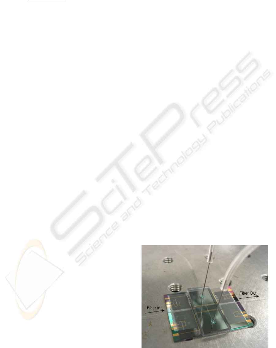
Metal capillaries with OD 400 μm and ID 200
μm were inserted through the PDMS to create liquid
inlet and outlet ports. Multimode optical fibers were
aligned to the on-chip waveguides through the use of
patterned grooves in the SU-8 resist. Once aligned
by hand under a stereomicroscope, an adhesive was
used to secure the fiber. The final packaged device is
shown in figure 2.
Figure 2: Photograph of packaged device.
BIODEVICES 2009 - International Conference on Biomedical Electronics and Devices
106
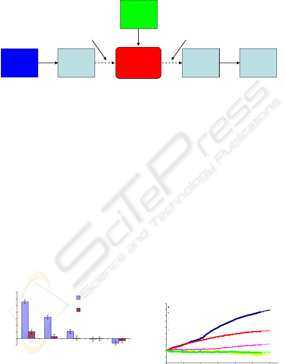
Microsensor
472 nm Blue
Laser
XYZ Fiber
Aligner Stage
Syringe Pump
Photodetector
Computer
Software
Input Fiber Output Fiber
Microsensor
472 nm Blue
Laser
XYZ Fiber
Aligner Stage
Syringe Pump
Photodetector
Computer
Software
Input Fiber Output Fiber
Figure 3: Block Diagram of testing setup for the MEMS sensor.
4 TESTING AND RESULTS
Absorbance measurements from catechol oxidation
were taken using blue light (472 nm) coupled
through the MEMS device. Figure 3 displays a
graphic of the testing setup used. Light was
delivered from a free space blue laser (LaserMate,
Pomona, CA) operating in the continuous wave
mode and focused into a multimode fiber using a
manual alignment stage. Output light was coupled
via the optical fiber to a USB linked
spectrophotometer (Ocean Optics, Dunedin, FL)
which facilitated automated data collection using
software. Catechol flakes were purchased from
Sigma Aldrich and dissolved in a 20 mM phosphate
buffer at a pH of 5.3. Liquid was administered using
a GENIE PLUS syringe pump (Kent Scientific,
Torrington, CT) at a flow rate of 100 μl/hr, which
translates to a linear flow velocity in the channel of
about 1 mm/s. All of the experiments were
performed at room temperature.
Figure 4 displays the change in measured light
intensity for three different catechol concentrations
after they were oxidized for 10 minutes at a current
density of 4A/m
2
. No decrease in intensity was
observed from the oxidation of the buffer solution or
-10
0
10
20
30
40
50
60
70
100 mM
Catechol
10 mM
Catechol
1 mM
Catechol
Buffer
Solution
100 mM
Ascorbic Acid
Decrease in Intensity (%)
with chitosan
without chitosan
Figure 4: Measured decrease in light intensity at 472 nm
after 10 minute oxidation at 4 A/m
2
. A clear signal
increase is displayed for all catechol concentrations when
using chitosan in the device.
the common antioxidant, ascorbic acid. Also shown
are measurements for devices without the chitosan
film. The data clearly demonstrates the necessity of
the chitosan in order to detect smaller concentrations
of catechol. Devices with the chitosan film display a
3x and 7x signal increase vs. those without chitosan
for 100 mM and 10 mM catechol concentrations
respectively. At our lowest measured concentration
of 1 mM, no change in the light intensity is detected
for the device without the chitosan film. The
chitosan film amplifies the signal because it
effectively traps the generated o-quinones at the
sensing area of the device through covalent bonding.
It should be noted that these tests without chitosan
require the liquid flow to be stopped in the channel.
Any applied flow rate will cause the o-quinones to
be swept away from the sensing area, disallowing
any accumulation which would cause a detectable
change in absorbance. Measurement error was
calculated based on the observed fluctuations in the
intensity measurement due to either changes in the
laser power or noise effects in the detector.
The increasing absorbance change over the 10
minute period for each sample is displayed in figure
5. The accumulation of the o-quinones is roughly the
same for each concentration of catechol for the first
minute as the rate is primarily reaction limited. Over
-0.1
-0.05
0
0.05
0.1
0.15
0.2
0.25
0.3
0.35
0.4
0 100 200 300 400 500 600
Time (sec)
Absorbance
100 mM Catechol
10 mM Catechol
1 mM Catechol
100 mM Ascorbic Acid
Buffer Solution
Figure 5: Change in absorbance over time for each sample.
CATECHOL DETETION USING AN OPTICAL MEMS SENSOR
107

time, the absorbance rate becomes diffusion limited
as the catechol must traverse through the chitosan
film to reach the electrode.
5 CONCLUSIONS
We report the demonstration of on-chip catechol
detection using optical absorbance measurements.
The device successfully demonstrates selective
detection of phenolic (catechol) vs. non-phenolic
(ascorbic acid) compounds without the need of
enzymes. The device also exhibits good
differentiation for a wide range of catechol
concentrations. Since our device uniquely allows for
the collection of time resolved absorbance data,
calibration curves can be fit to different times in
order to achieve more accurate sensing of the
concentration. The analysis performed in this
research can hopefully help to provide the
groundwork for a device used for the detection of
catechol packaged in a low-cost, portable system.
ACKNOWLEDGEMENTS
The authors would like to thank the National
Science Foundation (NSF-EFRI) and the R. W.
Deutsch Foundation for funding this research.
REFERENCES
Abdullah, J., Ahmad, M., Karuppiah, N., Heng, L. Y. &
Sidek, H. (2006) Immobilization of tyrosinase in
chitosan film for an optical detection of phenol.
Sensors and Actuators B, 114, 604-609.
Powers, M. A., Koev, S. T., Schleunitz, A., Yi, H.,
Hodzic, V., Bentley, W. E., Payne, G. F., Rubloff, G.
W. & Ghodssi, R. (2005) A fabrication platform for
electrically mediated optically active biofunctionalized
sites in BioMEMS. Lab on a Chip, 5, 583-586.
Shan, D., Zhu, M., Han, E., Xue, H. & Cosnier, S. (2007)
Calcium carbonate nanoparticles: A host matrix for the
construction of highly sensitive amperometric phenol
biosensor. Biosensors and Bioelectronics, 23, 648-
654.
Sies, H. (1997) Oxidative stress: oxidants and
antioxidants. Experimental Physiology, 82, 291-295.
Starek, A. (2003) Estrogens and Organochlorine
Xenoestrogens and Breast Cancer Risk. International
Journal of Occupational Medicine and Environmental
Health, 16, 113-124.
Wu, L.-Q., Ghodssi, R., Elabd, Y. A. & Payne, G. F.
(2005) Biomimetic Pattern Transfer. Advanced
Functional Materials, 15, 189-195.
Wu, X. J., Choi, M. M. F. & Wu, X. M. (2004) An
organic-phase optical phenol biosensor coupling
enzymatic oxidation with chemical reduction. The
Analyst, 129, 1143-1149.
Yi, H., Wu, L.-Q., Bentley, W. E., Ghodssi, R., Rubloff,
G. W., Culver, J. N. & Payne, G. F. (2005)
Biofabrication with chitosan. Biomacromolecules, 6,
2881-2894.
BIODEVICES 2009 - International Conference on Biomedical Electronics and Devices
108
