CARRIER AND SYMBOL PHASE SYNCHRONIZERS
Antonio D. Reis
1,2
, Jose F. Rocha
1
, Atilio S. Gameiro
1
and Jose P. Carvalho
2
1
Dep. de Electrónica e Telecomunicações / Instituto de Telecomunicações, Universidade de Aveiro, 3810 Aveiro, Portugal
2
Dep. de Fisica / U. D. Remota, Universidade da Beira Interior Covilhã, 6200 Covilhã, Portugal
Keywords: Synchronism, Telecommunications, Digital Communications.
Abstract: This paper presents two groups of synchronizers, namely the Carrier Phase Synchronizer and the Symbol
Phase Synchronizer. In the first group the VCO (Voltage Controlled Oscillator) synchronizes with the input
periodic signal and in the second the VCO synchronizes with a no periodic signal. Each group is studied
under four topologies, namely the analog, hybrid, combinational and sequential. The objective is to evaluate
the two groups with their four topologies and to observe the jitter-noise behaviours.
1 INTRODUCTION
This work study two groups of synchronizers,
namely the carrier phase synchronizers and the
symbol phase synchronizers (Jazwinski, 1966),
(Imbeaux, 1983).
The difference between the two groups is inside
of the phase comparator. So, the carrier phase
comparator synchronizes its VCO with an input
periodic deterministic wave, whereas the symbol
phase comparator synchronizes its VCO with an
input no periodic random symbol data sequence
(Rosenkranz, 1982), (Witte, 1983), (Hogge, 1985).
The carrier synchronizer recoveries the carrier and
the base band electric signal that is carried. The
symbol synchronizer recoveries the clock and uses it
to sample and to retime the data (Simon and
Lindsey, 1977), (Carruthers, Falconer, Sandler and
Strawczynski, 1990), (Huber and Liu, 1992),
(D’Amico, D’Andrea and Regianni, 2001), (Dobkin,
Ginosar and Sotiriou, 2004), (Noels, Steendam and
Moeneclaey, 2006).
Each group is studied under four topologies,
namely the analog, the hybrid, the combinational
and the sequential.
Also the difference between the four topologies is
inside of the phase comparator. Each phase
comparator uses its type of components (Reis,
Rocha, Gameiro and Pacheco, 2007).
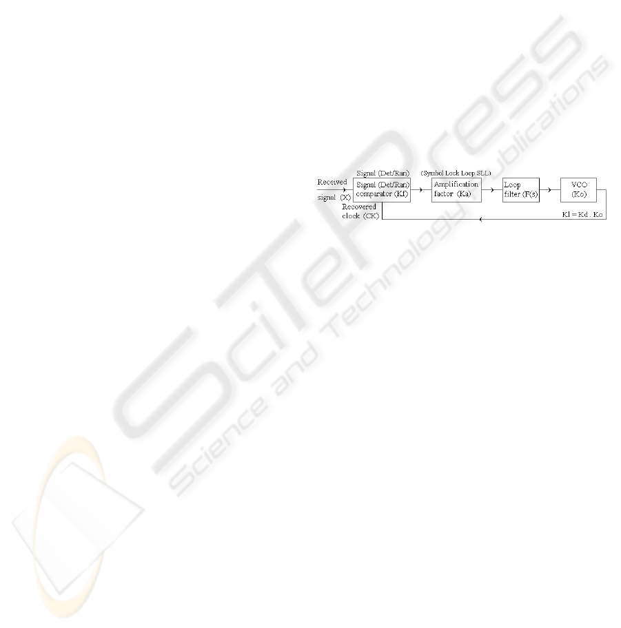
The synchronizer consists of the phase
comparator (phase Detector), loop filter, VCO and
amplification gain (Fig.1)
Figure 1: Aspect of the carrier and symbol phase
synchronizer.
Kf is the phase comparator gain, F(s) is the loop
filter, Ko is the VCO gain, and Ka is the loop
amplification gain that acts in the locus root
determining the desired characteristics.
Next, we present separately the two synchronizers
groups, beginning with the carrier group with their
four topologies and after the symbol group with their
four topologies.
Then, we present the design and tests of the two
groups with their four topologies.
After, we present the results with some
comparisons.
Finally, we present the conclusions.
2 FOUR CARRIER PHASE
SYNCHRONIZERS
We will present the four carrier phase synchronizers,
namely the analog, the hybrid, the combinational
and the sequential. The difference between them is
inside of the phase comparator (Reis, Rocha,
Gameiro and Pacheco, 2007).
186
D. Reis A., F. Rocha J., S. Gameiro A. and P. Carvalho J. (2008).
CARRIER AND SYMBOL PHASE SYNCHRONIZERS.
In Proceedings of the International Conference on Wireless Information Networks and Systems, pages 186-190
DOI: 10.5220/0002026701860190
Copyright
c
SciTePress
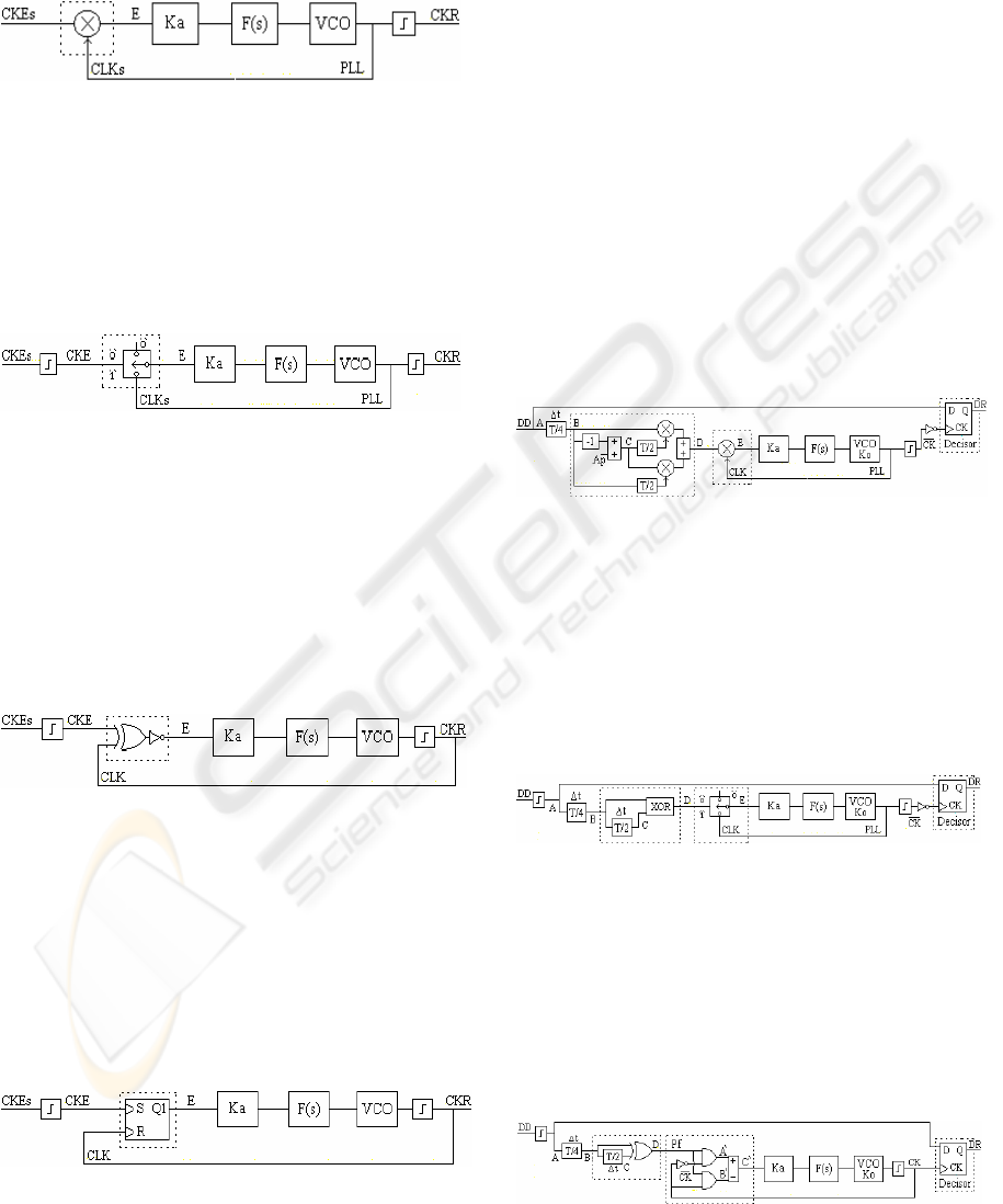
2.1 Analog Carrier Topology
The analog type has a carrier phase comparator
based on the ideal multiplier (analog component)
(Fig.2)
Figure 2: Analog carrier phase synchronizer.
The phase comparator two inputs (main input and
VCO output) are both analog (full-analog).
2.2 Hybrid Carrier Topology
The hybrid type has a carrier phase comparator
based on the real switch (hybrid component) (Fig.3)
Figure 3: Hybrid carrier phase synchronizer.
The phase comparator main input is digital but the
input coming from VCO output is still analog (semi-
analog).
2.3 Combinational Carrier Topology
The combinational type has a carrier phase
comparator based on an exor gate (combinational
component) (Fig.4)
Figure 4: Combinational carrier phase synchronizer.
The phase comparator two inputs (main input and
VCO output) are both digital, but the phase
comparator output is only function of the inputs
(digital combinational).
2.4 Sequential Carrier Topology
The sequential type has a carrier phase comparator
based on the flip flop (sequential component) (Fig.5)
Figure 5: Sequential carrier phase synchronizer.
The phase comparator two inputs (main input and
VCO output) are both digital, but now the phase
comparator output is simultaneously function of the
inputs and of its state (digital sequential - with intern
memory).
3 FOUR SYMBOL PHASE
SYNCHRONIZERS
We will present the four symbol phase
synchronizers, namely the analog, hybrid,
combinational and sequential. The difference
between them is inside of the phase comparator
(Reis, Rocha, Gameiro and Pacheco, 2007).
3.1 Analog Symbol Topology
Fig.6 shows the analog type, whose phase
comparator is based on analog ideal switches.
Figure 6: Analog symbol phase synchronizer.
The two inputs (main input and VCO output) at
the symbol phase comparator are both analog (full-
analog).
3.2 Hybrid Symbol Topology
Fig.7 shows the hybrid type, whose phase
comparator is based on an hybrid real switch.
Figure 7: Hybrid symbol phase synchronizer.
The two inputs (main input and VCO output) at
the symbol phase comparator, the first is digital, but
the second is still analog (half-analog).
3.3 Combinational Symbol Topology
Fig.8 shows the combinational type, whose phase
comparator is based on an exor gate.
Figure 8: Combinational symbol phase synchronizer.
CARRIER AND SYMBOL PHASE SYNCHRONIZERS
187
The two inputs (main input and VCO output) at
the symbol phase comparator are both digital
(digital-combinational). The output is only function
of the inputs (circuit without memory).
3.4 Sequential Symbol Topology
Fig.9 shows the sequential type, whose phase
comparator is based on a flip flop and additional
logic gates.
Figure 9: Sequential symbol phase synchronizer.
The two inputs (main input and VCO output) at
the symbol phase comparator are both digital
(digital-sequential). The output is simultaneously
function of the inputs and of the state (circuit with
memory).
4 DESIGN, TESTS AND RESULTS
We will present the design, tests and results of the
referred synchronizers (Reis, Rocha, Gameiro and
Pacheco, 2001).
4.1 Design
To get guaranteed results, it is necessary to
dimension all the synchronizers with equal
conditions. Then it is necessary to design all the
loops with identical linearized transfer functions.
The general loop gain is Kl=Kd.Ko=Ka.Kf.Ko
where Kf is the phase comparator gain, Ko is the
VCO gain and Ka is the control amplification factor
that permits the desired characteristics.
For analysis facilities, we use a normalized
transmission rate tx=1baud, what implies also
normalized values for the others dependent
parameters. So, the normalized clock frequency is
fCK=1Hz.
We choose a normalized external noise bandwidth
Bn = 5Hz and a normalized loop noise bandwidth Bl
= 0.02Hz. Later, we can disnormalize these values to
the appropriated transmission rate tx.
Now, we will apply a signal with noise ratio SNR
given by the signal amplitude Aef, noise spectral
density No and external noise bandwidth Bn, so the
SNR = A
2
ef
/(No.Bn). But, No can be related with the
noise variance σn and inverse sampling Δτ=1/Samp,
then No=2σn
2
.Δτ, so SNR=A
2
ef
/(2σn
2
.Δτ.Bn) =
0.5
2
/(2σn
2
*10
-3
*5)= 25/σn
2
.
After, we observe the output jitter UI as function
of the input signal with noise SNR. The dimension
of the loops is
- 1
st
order loop:
The loop filter F(s)=1 with cutoff frequency 0.5Hz
(Bp=0.5 Hz is 25 times bigger than Bl=0.02Hz)
eliminates only the high frequency, but maintain the
loop characteristics.
The transfer function is
H(s)=
G(s)
1G(s)+
=
+
=
+
KdKoF s
sKdKoFs
KdKo
sKdKo
()
()
(1)
the loop noise bandwidth is
Bl =
KdKo
Ka
K
fKo
44
=
= 0.02Hz (2)
Then, for the analog synchronizers, the loop
bandwidth is
Bl=0.02=
(Ka.Kf.Ko)/4 with (Km=1, A=1/2, B=1/2;
Ko=2π)
(Ka.Km.A.B.Ko)/4 = 0.02
-> Ka=0.08*2/
π
(3)
For the hybrid synchronizers, the loop bandwidth is
Bl=0.02=
(Ka.Kf.Ko)/4 with (Km=1, A=1/2, B=0.45;
Ko=2π)
(Ka.Km.A.B.Ko)/4 = 0.02
-> Ka=0.08*2.2/
π
(4)
For the combinational synchronizers, the loop
bandwidth is
Bl=0.02=
(Ka.Kf.Ko)/4 with (Kf=1/π; Ko=2π)
(Ka*1/
π
*2
π
)/4 = 0.02 -> Ka=0.04 (5)
For the sequential synchronizers, the loop bandwidth
is
Bl=0.02=
(Ka.Kf.Ko)/4 with (Kf=1/2π; Ko=2π)
(Ka*1/2
π
*2
π
)/4 =0.02 -> Ka=0.08 (6)
The jitter depends on the RMS signal Aef, on the
power spectral density No and on the loop noise
bandwidth Bl.
For analog PLL the jitter is
σφ
2
=Bl.No/Aef
2
=Bl.2.σn
2
.Δτ=0.02*10
-
3
*2σn
2
/0.5
2
=16*10
-5
.σn
2
For the others PLLs the jitter formula is more
complicated.
- 2
nd
order loop:
The
second order loop is not shown here, but the
results are identical to the ones obtained above for
the first order loop.
WINSYS 2008 - International Conference on Wireless Information Networks and Systems
188
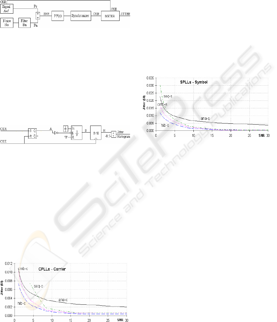
4.2 Tests
The following figure (Fig.10) shows the setup that
was used to test the various synchronizers.
Figure 10: Block diagram of the test setup.
The receiver recovered clock with jitter is compared
with the emitter original clock without jitter, the
difference is the jitter of the received clock.
4.3 Jitter Measurer (Meter)
The jitter measurer (Meter) consists of a RS flip
flop, which detects the random variable phase of the
recovered clock (CKR), relatively to the fixed phase
of the emitter clock (CKE). This relative random
phase variation is the recovered clock jitter (Fig.11).
Figure 11: The jitter measurer (Meter).
The other blocks convert this random phase
variation into a random amplitude variation, which
is the jitter histogram.
Then, the jitter histogram is sampled and
processed by an appropriate program, providing the
unit interval root mean square jitter (UI-RMS) and
the unit interval peak to peak jitter (UI-PP).
4.4 Results
We present firstly the results (RMS jitter - SNR
signal to noise ratio) of the carrier group with its
four topologies and after the symbol group with its
four topologies.
Figure 12: Jitter-SNR curves of the four carrier
synchronizers (a,h,c,s).
Fig.12 shows the jitter-SNR curves of the four
carrier phase synchronizers, namely the analog (ana-
c), the hybrid (hib-c), the combinational (cmb-c) and
the sequential(seq-c).
We verify, that for high SNR, the synchronizers
without input limiter (ana) is disadvantageous over
the others with input limiter (hib, cmb, seq).
However for low SNR the synchronizer with intern
memory (seq) is slightly disadvantageous over the
others without intern memory (ana, hib, cmb). This
disadvantage can be minimized with a prefilter.
Fig.13 shows the jitter-SNR curves of the four
symbol phase synchronizers, namely the analog
(ana-s), the hybrid (hib-s), the combinational (cmb-
s) and the sequential (seq-s).
Figure 13: Jitter-SNR curves of the four symbol
synchronizers (a,h,c,s).
We verify that for high SNR, the synchronizers
without input limiter (ana) is disadvantageous over
the others with input limiter (hib, cmb, seq). For low
SNR, the synchronizer with intern memory (seq) is
slightly disadvantageous over the others without
intern memory (ana, hib, cmb). This disadvantage
can be minimized with a prefilter.
5 CONCLUSIONS
We studied two groups of synchronizers, which are
the carrier phase synchronizers and the symbol
phase synchronizers, depending on their phase
comparator.
Each group was studied under four topologies,
namely the analog (ana), the hybrid (hib), the
combinational (cmb) and the sequential (seq).
The two groups present a similar results relation
between their four topologies (analog, hybrid,
combinational and sequential).
For high SNR, the synchronizer without input
limiter (ana) is disadvantageous over the others with
input limiter (hib, cmb, seq), since the limiter
ignores low noise spikes, diminishing the jitter.
For low SNR the synchronizers without input
CARRIER AND SYMBOL PHASE SYNCHRONIZERS
189

limiter (ana) becomes advantageous over the others
with input limiter (hib, cmb, seq), since the limiter
provokes random gate commutation, increasing the
jitter. Also, in low SNR the synchronizer with intern
memory (seq) is the worst case since the state
memory is scrambled by noise spikes increasing the
jitter. This disadvantage can be minimized with a
prefilter which reduces the noise spikes.
Anyway, the sequential topology, due to its intern
memory, has more project potentialities, what is
useful.
ACKNOWLEDGEMENTS
The authors are grateful to the program FCT
(Foundation for sCience and Technology).
REFERENCES
Jazwinski A. H., 1966. Filtering for Nonlinear Dynamical
Systems. IEEE Transactions on Automatic Control
p.765 Oct.
Imbeaux, J. C., 1983. Performance of the delay-line
multiplier circuit for clock and carrier synchronization.
IEEE Journal on Selected Areas in Communications
p.82 Jan.
Rosenkranz, W., 1982. Phase Locked Loops with limiter
phase detectors in the presence of noise. IEEE Trans.
on Communications com-30 Nº10 pp.2297-2304. Oct.
Witte, H. H., 1983. A Simple Clock Extraction Circuit
Using a Self Sustaining Monostable Multivibrator
Output Signal. Electronics Letters, Vol.19, Is.21,
pp.897-898, Oct.
Hogge, C. R., 1985. A Self Correcting Clock Recovery
Circuit. IEEE Tran. Electron Devices p.2704 Dec.
Reis, A. D., Rocha, J. F., Gameiro, A. S., Carvalho, J. P.,
2001. A New Technique to Measure the Jitter. Proc.
III Conf. on Telecommunications pp.64-67 FFoz-PT
23-24 Apr.
Simon, M. K., Lindsey, W. C., 1977. Tracking
Performance of Symbol Synchronizers for Manchester
Coded Data. IEEE Transactions on Communications
Vol. com-2.5 Nº4, pp.393-408, April.
Carruthers, J., Falconer, D., Sandler, H., Strawczynski, L.,
1990. Bit Synchronization in the Presence of Co-
Channel Interference. Proc. Conf. on Electrical and
Computer Engineering pp.4.1.1-4.1.7, Ottawa-CA 3-6
Sep.
Huber, J., Liu, W., 1992. Data-Aided Synchronization of
Coherent CPM-Receivers. IEEE Transactions on
Communications Vol.40 Nº1, pp.178-189, Jan.
D’Amico, A., D’Andrea, A., Reggianni, 2001. Efficient
Non-Data-Aided Carrier and Clock Recovery for
Satellite DVB at Very Low SNR. IEEE Jou. on
Sattelite Areas in Comm. Vol.19 Nº12 pp.2320-2330,
Dec.
Dobkin, R., Ginosar, R., Sotiriou, C. P., 2004. Data
Synchronization Issues in GALS SoCs. Proc. 10th
International Symposium on Asynchronous Circuits
and Systems, pp.CD-Ed., Crete-Greece 19-23 Apr.
Noels, N., Steendam, H., Moeneclaey, M., 2006.
Effectiveness Study of Code-Aided and Non-Code-
Aided ML-Based Feedback Phase Synchronizers.
Proc. IEEE Int Conf. on Comm.(ICC’06) pp.2946-
2951, Ist.-TK, 11-15 Jun.
Reis, A. D., Rocha, J. F., Gameiro, A. S., Carvalho, J. P.,
2007. Synchronizers Operating by Two or One Data
Transitions. Proc. V Sym. on Enabling Optical
Network and Sen. (SEONs 2007) p.87-88, Av-PT 29-
29 Jun.
WINSYS 2008 - International Conference on Wireless Information Networks and Systems
190
