DIFFERENTIAL ELECTRIC FIELD SENSITIVE FIELD EFFECT
TRANSISTOR
Characteristics, Modeling and Applications
Yehya H. Ghallab
1, 2
and Wael Badawy
2
1
Department of Biomedical Engineering, Helwan University, Cairo, Egypt
2
Department of Electrical and Computer Engineering,University of Calgary, Calgary, Alberta, Canada
Keywords: Electric Field Sensor, CMOS technology, Electric Field, Field Effect Transistor, lab-on-a-chip, Integrated
sensors.
Abstract: This paper presents the Differential Electric Field Sensitive Field Effect Transistor (DeFET) as a CMOS
electric field sensor. The DeFET is based on a standard 0.18-µm Taiwan Semiconductor Manufacturing
Company (TSMC) CMOS technology. This paper also presents the DeFET’s DC and AC models. The
experimental and simulation results which validate the different models of the DeFET are presented.
Moreover, some applications of the DeFET on the biomedical and lab-on-a-chip are presented.
1 INTRODUCTION
The Differential Electric Field Sensitive Field Effect
Transistor (DeFET) device is a new electric field
sensor which can sense the electric field and convert
the electric field into a corresponding electrical
signal such as voltage or current (Ghallab et al.,
2005) (Ghallab et al., 2006) Its physical structure
has two adjacent gate terminals (Ghallab et al.,
2005). With the split-gate structure, DeFET can
sense the electric field which is perpendicular to the
gate channels of the device. Using the DeFET, we
can get direct real-time information about the
electric field, and consequently, we can extract
useful information such as identify and characterize
the biological cells (Ghallab et al., 2006). Also, the
DeFET can be simply integrated with the CMOS-
based lab on a chip and read-out circuits. As a new
device, the DeFET is not a standard device in the
(Simulation Program with Integrated Circuit
Emphasis) SPICE simulator libraries, so we need a
macro model to evaluate the performance of circuits
composed of DeFET and MOSFET devices.
In this paper, SPICE macro models (dc and ac
models) of DeFET will be offered to evaluate the
performance of the circuits. Also, some applications
of the DeFET are presented.
This paper is constructed as follows. The
operational principle of the DeFET is reviewed in
part2. The SPICE macro models (dc and ac) are
formed and described in Section 3. Experimental
and simulation results which confirm the proposed
models are shown and discussed in part 4. Some
applications of the DeFET are presented in part 5.
Section 6 concludes this paper and discusses the
merits of the proposed DeFET based on the
experimental findings.
2 THE DeFET
The DeFET consists of two complementary eFETs,
one of them is a P eFET type and the second is an N
eFET type (Ghallab et al., 2006). The eFET structure
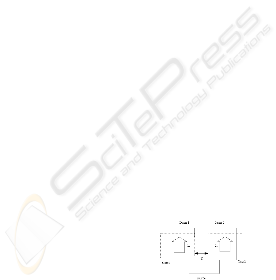
is shown in Fig. 1. The eFET contains two split
drains, two split gates and a single source, see Fig. 1.
Figure 1: Schematic structure of an DeFET.
The equivalent circuit of the DeFET is shown in Fig.
2.
250
H. Ghallab Y. and Badawy W. (2008).
DIFFERENTIAL ELECTRIC FIELD SENSITIVE FIELD EFFECT TRANSISTOR - Characteristics, Modeling and Applications.
In Proceedings of the First International Conference on Biomedical Electronics and Devices, pages 250-255
DOI: 10.5220/0001046102500255
Copyright
c
SciTePress
Figure 2: An equivalent circuit of a DeFET and schematic
of the DeFET used in SPECTRE simulation.
From Fig. 2, the two gates of P eFET and N eFET
are connected with each other, and there is a cross
coupling between the two drains of the P eFET and
the N eFET. The output current I
Out
is equal to the
difference between the two drain currents Ip-In (i.e.
I
Out
= Ip-In, see Fig.2). On the other hand, Ip and In
are functions of the two applied gate voltages V
in1
and V
in2
, respectively. The DeFET is designed to
achieve an output voltage V
Out
, directly related to the
difference between the two applied gate voltages
(V
in1
-V
in2
), and as V
in1
-V
in2
is equal to the applied
electric field above the two gates (E) multiplied by
the distance between them (V
in1
-V
in2
/Y = E), where
Y is the distance between the two split gates, which
is constant. So, V
Out
is related directly to the intensity
of the applied electric field. Thus by measuring V
Out
we can detect the intensity of the electric field to be
as follows (Ghallab et al., 2006):
Ou t m L Un i
VgYREV=+
(1)
Eq. 1 shows a liner relationship between the
DeFET’s output voltage and the intensity of the
applied electric field.
Also, from Eq. 1, we can observe that there is two
cases, they are:
1) Null electric-field case (Uniform case): This
special case will be obtained when the intensity of
the electric filed is zero, and consequently getting
the same potential on the two gates (i.e., V
in1 = Vin2),
and from Eq.1V
out
=V
uni
2) Nonzero electric-field case (Nonuniform case):
This implies any electric-field condition that leads to
a potential difference between the two gates (i.e.,
V
in1 ≠Vin2). So, we can rewrite Eq. 1 as:
out Non Uni
V=V +V
(2)
where: V
non
= SE=
mL
g
YR E
is the output voltage
when we have a nonuniform electric field case, and
V
uni
is the output voltage when we have a uniform
electric field case and S (sensitivity) =
mL
g
YR
.
3 MODELING THE DeFET
As a new device, the DeFET is not a standard device
in the simulator libraries, so a macro model to
evaluate the performance of circuits composed of
DeFET and MOSFET devices is needed. A Dc
model has been proposed and tested using
SPECTRE version 5. Also, an equivalent dc circuit
of the DeFET using PSPICE version 9.1 have
proposed. So, it can be used in the SPICE
environment.
3.1 A Simple DC Model
Fig. 2 shows the proposed DeFET circuit used for
SPECTRE simulation. The channel length and the
width of the Pmos and Nmos used are 0.4μm / 10μm
and 0.4μm / 1μm, respectively. Fig. 3 shows the
simulation results of the output voltage V
Out
against
the input voltage difference V
in1
- V
in2
(∆V), where
V
in1
varies from –2.5V to 2.5V and V
in2
is 0V.
Figure 3: DC response of the DeFET.
From Fig. 3, a linear relationship between V
Out
and
∆V can be observed. As the external electric field
E= -∆V/Y, and Y=0.5μm, Fig.4 shows the output
voltage V
Out
against the intensity of the applied
electric field. We can observe that V
Out
is linearly
related to E, as we expected from the theory of the
DeFET (see Eq. 1). The sensitivity can be
determined from this figure as S= ∆V
out
/∆E =
51.7(mV/V/μm). If we vary V
in1
from –2.5 to 2.5
Volt
and V
in2
from –3 to 3Volt, we can get the same
DIFFERENTIAL ELECTRIC FIELD SENSITIVE FIELD EFFECT TRANSISTOR - Characteristics, Modeling and
Applications
251
linear relationship between V
Out
and V
in1
for
different V
in2
, as shown in Fig. 5.
-4.0E+006 -2.0E+006 0.0E+000 2.0E+006 4.0E+006
0.4
0.6
0.8
1
0.5
0.7
0.9
Figure 4: Output voltage versus electric field intensity.
-2 -1 0 1 2-2. 5 -1.5 -0.5 0.5 1. 5 2. 5
-1
-0. 5
0
0.5
1
1.5
2
-0.75
-0.25
0.25
0.75
1.25
1.75
V
in2
= -3V
V
in2
= -2V
V
in2
= -1V
V
in2
= 0V
V
in2
= 1V
V
in2
= 2V
V
in2
= 3V
Figure 5: Spectre’s simulation results.
3.2 SPICE’s DC Equivalent Circuit
Fig. 6 shows the SPICE equivalent circuit of the
DeFET. As it is outlined before in The DeFET’s
theory of operation (section 2), there are two cases
of electric field. The first one is a uniform electric
field case, and the second is a nonuniform electric
field, both of these field cases can control the output
voltage (V
out
). The output voltage caused by the
uniform case (V
uni
) is represented by the four
MOSFETs (M
1
-M
4
) with the two gates are
connected, see Fig. 6. In other words, V
Uni
represents
the output voltage when the two gates are connected.
The output crrent caused by a nonuniform electric
field (I
Non
), is represented by an electric field
controlled current source (ECCS). I
Non
is related to
the electric field E, and the sensitivity S by the
equation (I
Non
= SE).
V
DD
V
SS
M
1
M
2
M
3
M
4
V
in
I
p
I
n
V
o
ECCS
I
Non
I
Uni
R
L
Figure 6: DeFET’s SPICE equivalent circuit.
Fig. 7 shows the SPICE equivalent circuit of ECCS.
In this SPICE circuit, the external electric field
applied is represented as a voltage source V
Ele
. The
value of R
sen
is proportional to the inverse value of
the sensitivity “S”. I
Non
is a current source controlled
by I
1
, which caused by the nonuniform external
electric field.
Figure 7: Electric field controlled current source (ECCS)
model.
As a simple model, Fig. 8 shows this simple DC
model, where the output current (I
out
) is the
summation of two dependent sources of current.
The first is an electric field controlled current source
(I
Non
), which represents the nonumiform electric
field, and the second is a voltage controlled current
source (I
Uni
), which represents the output current
obtained when having a uniform electric field.
BIODEVICES 2008 - International Conference on Biomedical Electronics and Devices
252
Figure 8: A simple DC model.
3.3 AC Model
Fig. 9 Shows the AC model of the DeFET, where
the media is represented by a capacitor in parallel
with a resistor (C
ext
//R
ext
). The media here can be the
dielectric fluid above the DeFET sensor, or any
neutral body, such as: biocells, DNA molecules, or
virus, or it can be both.
Figure 9: The AC model of the DeFET.
The AC response for different C
ext
values is shown
in Fig. 10. From this figure we can observe that the
DeFET is working as a bandpass filter. The
magnitude, bandwidth and the frequency range of
operation of this filter depend on the external media;
see Fig. 9, these factors are very important to extract
useful information about the media itself. A
summary of these results is shown in Table 1.
Figure 10: AC response with Rext =500K Ohm and Cext
varies (Ghallab et al., 2006).
Table 1: Summary of the AC response when R
ext
=500 KΩ
and C
ext
varies.
C
ext
Central frequency Bandwidth
10 pF
0.1 nF
100 nF
1µF
26.7 MHz
10 MHz
2.6 MHz
50.1 KH
116 MHz
26.59 MHz
9.84 MHz
311 KHz
4 SIMULATION AND
EXPERIMENTAL RESULTS
Fig. 11 shows the schematic input file for the
PSPICE, we have used level 7 models for the used
Pmos and Nmos transistors. Fig. 12 shows the
simulation results of the output voltage V
Out
against
the input voltage V
3
, where V
3
varies from –2.5V to
2.5V and V
4
varies from –3 to 3Volt. From Fig. 12,
V
3
represents the uniform electric field source, while
V
4
represents the nonuniform electric field source.
Also we can observe the linear relationship between
V
Out
and V
in1
for different V
in2
. In Fig. 12, both the
simulation results obtained from the two different
models that were proposed, i.e. using PSPICE and
SPECTRE simulators, and we can observe the good
agreements between these two models. Thus, both of
these models can properly represent the DC response
of the DeFET.
Nonuniform electric field source
Uniform electric
Field source
Figure 11: DeFET’s PSPICE equivalent circuit.
As the external electric field E = -∆V/Y, and
Y=0.5μm, Fig. 13 shows the output voltage V
Out
against the electric field applied. We can observe
that V
Out
is linearly related to E, as we expected
from the theory of the DeFET (see equation 1).
DIFFERENTIAL ELECTRIC FIELD SENSITIVE FIELD EFFECT TRANSISTOR - Characteristics, Modeling and
Applications
253
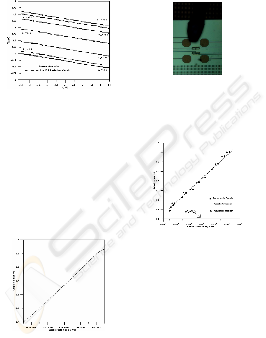
Figure 12: SPECTRE and PSPICE simulation.
As the external electric field E = -∆V/Y, and
Y=0.5μm, Fig. 13 shows the output voltage V
Out
against the electric field applied. We can observe
that V
Out
is linearly related to E, as we expected
from the theory of the DeFET (see equation 1).
The proposed DeFET is implemented in the
standard CMOS 0.18-µm technology. Fig. 14 shows
a microscopic picture of two DeFETs and the
electrodes used to apply the required electric-field
pattern. To test experimentally the DC response of
the DeFET, a DC voltage with different values,
signs and different configuration have been applied
to the four electrodes surrounding the DeFET
sensors, hence, varying the magnitude and sign of
the applied electric field (E) (Ghallab et al., 2006).
At the output, the output voltage associated with
each value of the measured electric field above the
gates will be measured and compared with the
simulation results, i.e., Specter’s circuit Simulator.
Figure 13: PSPICE Output voltage versus electric field
intensity.
Figure 14: The die picture shows the DeFET sensor
(Ghallab et al., 2006).
The result is shown in Fig.15, from which a good
agreement between the experimental and the
simulation results can be observed. Also, we can
observe that the sensitivity of the DeFET, which is
the slope of the line shown in Fig. 15, is about
51.7mV/ (V/µm).
Figure 15: The DC response of the DeFET (Ghallab,
2005).
5 DeFET’S APPLICATIONS
Differential Electric Field Effect Transistor (DeFET)
sensor can be used in many applications: for
example, it can be used in microfluidic applications,
to extract some useful properties of the fluid that is
used. Also; it can be used in nonuniform electric
field (Dielectrophoresis) applications to get
information about the biocells that are used. To
achieve this (Burt et al, 1989), DeFET can measure
the disturbance that occurs from the existence of the
biocells in the applied electric field; it is well known
that each kind of biocell will provide a different
disturbance based on its electrical properties, i.e. its
conductivity and permittivity
.
Moreover, if we use
the DeFETs in array form, i.e., array of sensors, then
BIODEVICES 2008 - International Conference on Biomedical Electronics and Devices
254

we can sense the electric field at different locations.
In its array form, the proposed DeFET sensor can be
applied to the DNA analysis, because we can use it
to detect the radius of the DNA molecule (Washizu
M. et al, 1990).
6 CONCLUSIONS
This paper presents the characteristics and the
alternative models of the DeFET, as a new electric
field sensor. Although DeFET is not a standard
device in the SPICE library, the macro models for
the DeFET device is presented to evaluate the
performance of circuits composed of the MOSFET
and DeFET devices. The experimental results have
been compared with the simulation results of the
proposed models. The correctness and flexibility of
the proposed SPICE models have been verified. The
proposed methods are expected to make the
prediction of the circuits using the DeFET and
MOSFET devices possible. The proposed DeFET
sensor can be used in many applications in the
biomedical field.
REFERENCES
Ghallab, Y. H. and Badaw, W. 2006, ‘DeFET, A Novel
Electric field Sensor for Lab-on-a-Chip and
Biomedical Applications’, IEEE Journal of Sensor,
vol.6, no.4, pp. 1027-1037.
Ghallab, Y. H. and Badawy, W. 2006, ‘A Single CMOS
Chip for Biocell Tracking, Levitation, Detection, and
Characterization’, International symposium on Circuit
and system (ISCAS 06), pp. 3349-3352.
Ghallab, Y. H. and Badawy, W. 2005, ‘A CMOS Lab-on-
a-Chip for Biomedical Applications’, International
symposium on Circuit and systems (ISCAS 05), pp.
1346-1349.
Ghallab, Y. H. 2005, ‘A Novel CMOS Electric Field
Imager for Lab-on-a-chip and Biomedical
Applications’, PhD Thesis, University of Calgary,
Canada.
Burt J. P. H., Al-Ameen T. A. K., Pethig R., and Wang
X., 1989, “An optical dielectrophoresis spectrometer
for low frequency measurements on colloidal
suspensions,” J. Phys. E, Sci. Instrum., vol. 22, no. 11,
pp. 952–957.
Washizu M. and Kurosawa O. 1990, “Electrostatic
manipulation of DNA in microfabricated structures,”
IEEE Trans. Ind. Appl., vol. 26, no. 6, pp. 1165–1172.
DIFFERENTIAL ELECTRIC FIELD SENSITIVE FIELD EFFECT TRANSISTOR - Characteristics, Modeling and
Applications
255
