
TRACKING PLASMA ETCH PROCESS VARIATIONS USING
PRINCIPAL COMPONENT ANALYSIS OF OES DATA
Beibei Ma, Seán McLoone and John Ringwood
Department of Electronic Engineering, National University of Ireland Maynooth, Maynooth, Ireland
Keywords: Semiconductor manufacturing, plasma etching, metal etching, optical emission spectroscopy (OES),
principal component analysis (PCA), batch processing.
Abstract: This paper explores the application of principal component analysis (PCA) to the monitoring of within-lot
and between-lot plasma variations that occur in a plasma etching chamber used in semiconductor
manufacturing, as observed through Optical Emission Spectroscopy (OES) analysis of the chamber exhaust.
Using PCA, patterns that are difficult to identify in the 2048-dimension OES data are condensed into a
small number of principle components (PCs). It is shown, with the aid of experimental data, that by simply
tracking changes in the directions of these PCs both inter-lot and intra-lot patterns can be identified.
1 INTRODUCTION
Modern day semiconductor manufacturing is a
highly competitive business in which companies are
required to produce vast quantities of reliable high
performance integrated circuits (ICs) at low cost. As
such, close monitoring and tight control of hundreds
of complex process steps are needed to maintain
production standards and high product throughput.
In this context we focus on plasma etching of
semiconductor wafers, an important process step in
the manufacture of many ICs (Sugawara, 1998). A
typical reaction ion etching (RIE) chamber is
illustrated in Fig. 1. Gas is pumped into the chamber
under vacuum and ionised using a high power
Microwave (MF) source to create a plasma. A radio
frequency (RF) electromagnetic field accelerates the
resulting ionised species towards the electrode,
where they interact both chemically and physically
with the wafer, etching away the exposed surface.
The etch rate and profile obtained are determined in
a complex and nonlinear fashion by the plasma
chemistry and energy as well as several process
variables including gas flow rates and RF power.
Monitoring the chemistry of the plasma in the
chamber can be achieved using Optical Emission
Spectroscopy (OES) (Splichal et al., 1987). In the
plasma chamber considered in this study the OES
data is collected for the exhaust plasma leaving the
chamber using a 2048 wavelength OES sensor
(170nm to 875nm) with a sampling interval of 0.75s.
Using this setup OES data was collected for 17 lots
of 24 wafers, with each waver undergoing a two step
etch process lasting 45s. A sample OES data set for
a single wafer is shown in Fig. 2.
Exhaust
MF
Plasma
BCl
3
, Cl
2
Wafer
Electrode
RF
Match
box
OES
Figure 1: Diagram of a plasma etching chamber.
With the OES footprint of each wafer having
dimensions of 60
×
2048, direct visualisation and
monitoring of variations in the plasma chemistry
across wafers and across lots is impractical.
Fortunately, optical emission spectra are inherently
highly redundant making it possible to achieve
substantial data compression using Principle
Component Analysis (PCA) techniques without
loosing valuable information on plasma changes. In
this paper we show that simply monitoring changes
361
Ma B., McLoone S. and Ringwood J. (2007).
TRACKING PLASMA ETCH PROCESS VARIATIONS USING PRINCIPAL COMPONENT ANALYSIS OF OES DATA.
In Proceedings of the Fourth International Conference on Informatics in Control, Automation and Robotics, pages 361-364
DOI: 10.5220/0001629303610364
Copyright
c
SciTePress
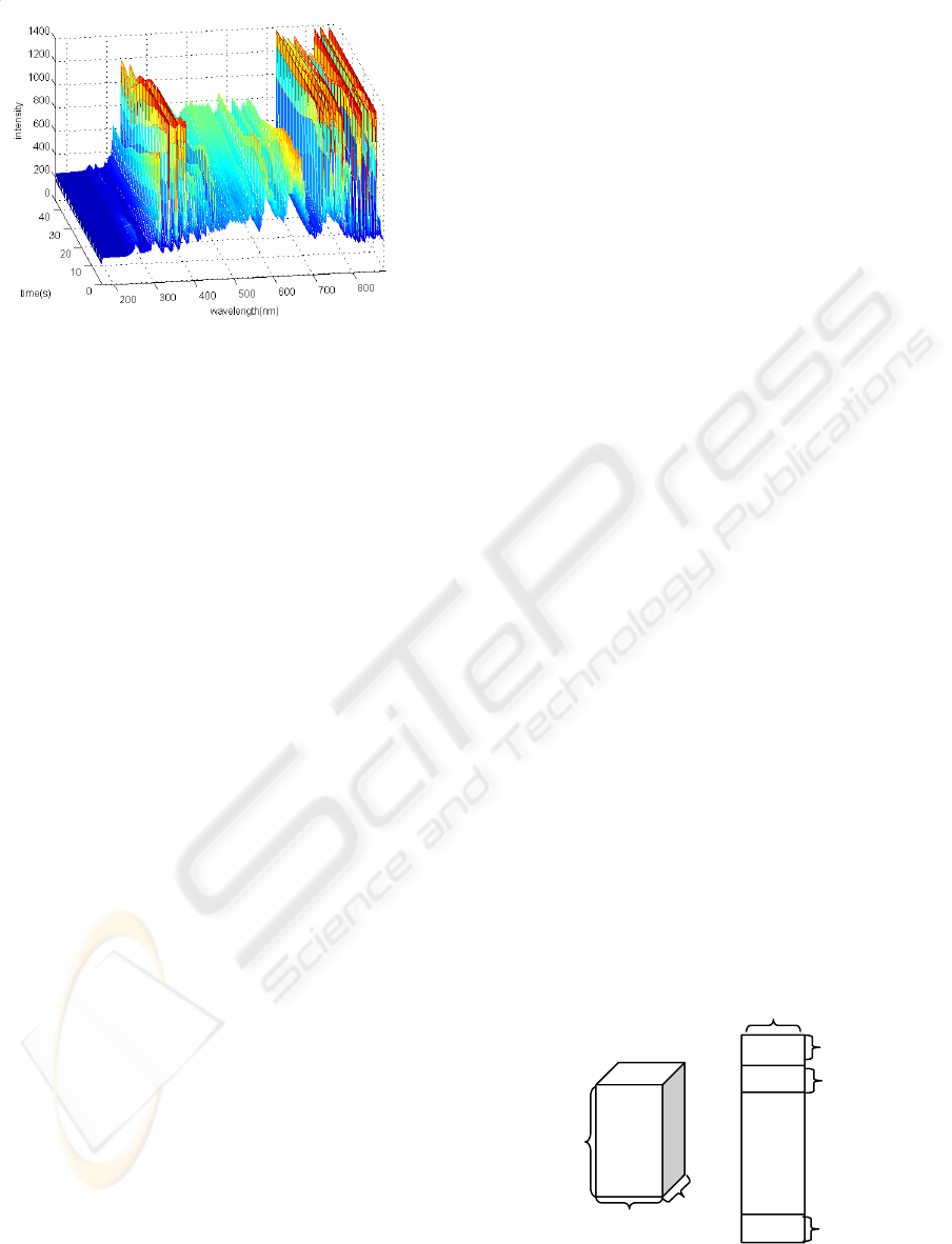
Figure 2: A plasma etch OES data set for a single wafer.
in the directions of the principle component loading
vectors, computed on either a wafer-by-wafer or lot-
by-lot basis, is sufficient to detect valuable
information on process trends that are not
immediately apparent when looking at the OES data
as a whole.
2 PRINCIPAL COMPONENT
ANALYSIS
Principal component analysis (PCA) is a linear
multivariate data projection technique widely used
for data compression and analysis (Jackson, 1991). It
provides a means of generating low dimension
representations of high dimension datasets while
retaining the maximum amount of information.
2.1 Definition
PCA is a method of writing a matrix X of rank r as
a sum of r matrices of rank 1,
where the rank 1
matrices are expressed as outer products of two
vectors, a score
i
t and a loading
i
p (Jackson, 1991)
∑
=
=
r
i
ii
1
T
ptX
(1)
The loading vectors,
i
p , are eigenvectors of the
matrix
XX
T
, that is
iii
ppXX
λ
=)(
T
(2)
where
i
λ is the eigenvalue associated with the i
th
eigenvector
i
p . The loading vectors
i
p describe the
principal directions of variation in X, are orthogonal
to each other:
ji
ji
≠∀= ,pp 0
T
(3)
and have unit length, while the eigenvalues indicate
the amount of variance represented by each
direction. For a given
X and
i
p , the corresponding
score vector
i
t is given by:
ii
Xpt
=
(4)
A principle component (PC) model of
X
is then
obtained by selecting the components
),(
ii
tp with
the largest eigenvalues to represent it. When data
redundancy is high two or three PCs are often
sufficient to obtain a good model.
Essentially, PCA projects a high dimensional
data space onto a lower dimensional sub-space
where the axes are the PC loading vectors and the
coordinates of the data the PC score vectors.
Singular Value Decomposition (SVD) can be
used to calculate all r principal components in one
step. Alternatively, the nonlinear iterative partial
least squares (NIPALS) algorithm (Geladi, 1986)
can be used to calculate them one at a time in order
of significance.
2.2 Multi-way PCA (MPCA)
Since batch process data is usually arranged in a 3-
way matrix (batch-variable-time), it must be
unfolded into a 2-way matrix in order to apply PCA.
This is known as Multi-way Principal Component
Analysis (MPCA) and was first introduced by Wold
et al. (1987). There are several ways to unfold a 3-
way matrix. In this paper, we choose to unfold the
data along wavelength direction (Fig. 3), because we
are interested in tracking process changes over time.
time
wavelength
wafer1
wafer24
wafer2
time
time
wavelength
24 wafers
time
Batch
Figure 3: Unfolding of the 3-way OES data blocks. Each
block corresponds to a lot of 24 wafers.
ICINCO 2007 - International Conference on Informatics in Control, Automation and Robotics
362
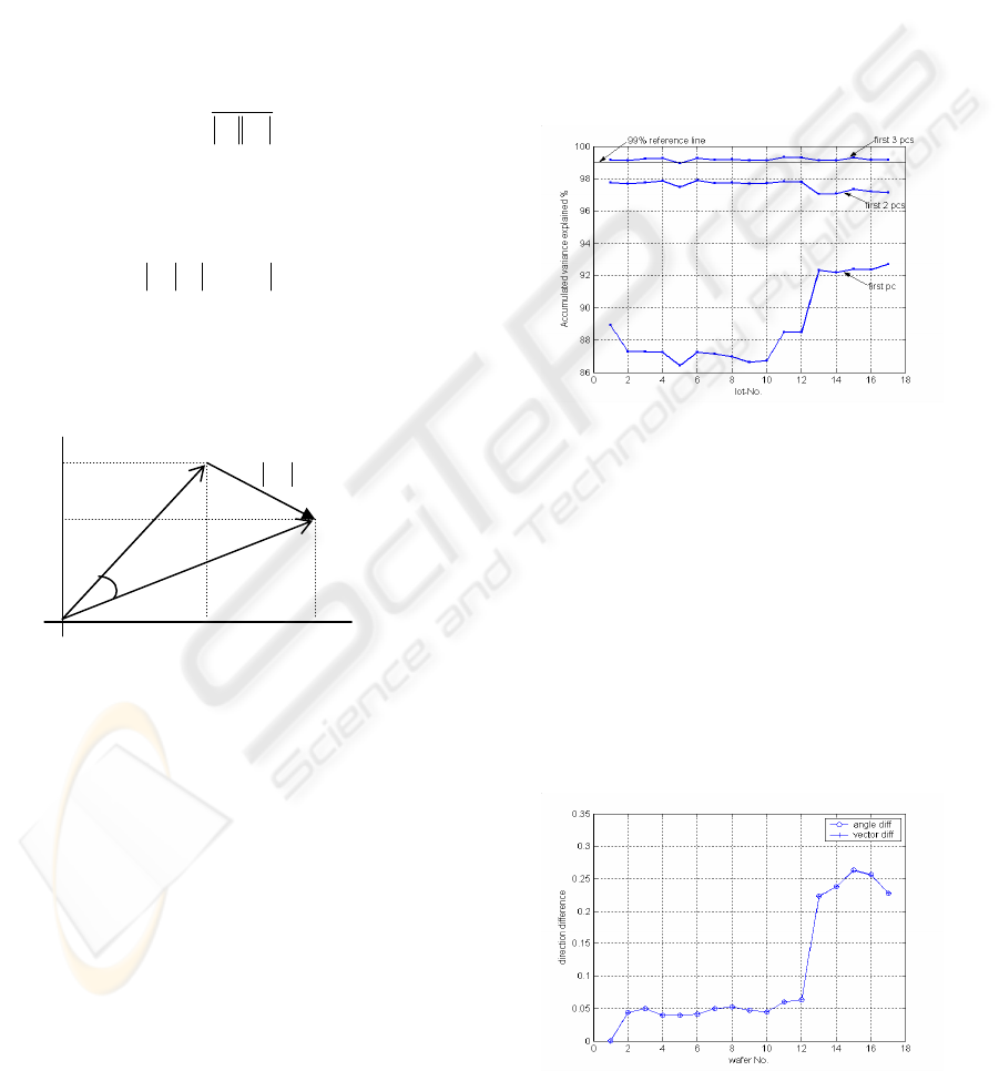
2.3 Monitoring PC-loadings
If PCA is performed on the OES data as a whole
process trends can only be observed by monitoring
the time evolution of the scores. However, if PCA is
applied on a wafer-by-wafer or lot-by-lot basis very
effective monitoring of process variation can be
achieved by tracking the changes in the directions of
the PC loadings. Changes can be expressed either in
terms the angle between loadings or the magnitude
of the vector difference between them as illustrated
in Fig. 4. The angle
θ (in radians) is given by
)
vv
vv
(
21
T
21
arccosθ =
(5)
while the magnitude of the vector difference
φ is
simply defined as
21
vvΔv −==φ .
(6)
Since, by definition, loading vectors are unit length
it follows that for small
θ the two measures are
approximately equivalent, i.e.
θφ ≈ .
Figure 4: Measuring changes in loading vector directions.
3 OES DATA ANALYSIS
3.1 Data Pre-processing
Data pre-processing is an essential first step in PCA
analysis. Variables need to be appropriately scaled
and irrelevant or corrupted measurements removed
if valid and interpretable results are to be obtained.
In this study the following pre-processing step were
performed on the OES data: (1) Data segments
corresponding to non-etch periods at the start and
end of each etch cycle were removed; (2) Saturated
wavelengths were omitted and; (3) Wavelength
intensities were scaled to have zero mean.
3.2 Lot-by-lot Analysis
Having unfolded the OES data as indicated in Fig. 3,
analysis by PCA can be performed by treating each
lot of 24 wafers as a single data matrix. We will
refer to the resulting PCs as lot-PCs, consisting of
lot-PC loadings and lot-PC scores. The variance
explained by the first three lot-PCs is plotted as a
function of lot number in Fig. 5. This shows that
across all lots the first three principal components
can explain over 99% of the plasma variation
captured by the OES data. In fact the first PC
captures over 85% of the data variation observed
across all 2048 wavelengths.
Figure 5: Accumulated variance explained by the first
three lot PCs.
A closer look at Fig. 5 shows that a jump occurs
in the variance explained by lot-PC
1
at lot 13.
Analysis of the variation in the direction of lot-PC
1
across lots (Fig. 6) reveals that this is linked to a
significant change in the orientation of lot-PC
1
from
lot 13 onwards. Following investigation it was
determined that the plasma change was as a result of
a small drift in the flow rate of a cooling gas applied
to the backside of the wafers during etching, a
change that was not detected by the existing plasma
chamber process monitoring schemes.
Figure 6: Variation in lot-PC
1
(loading) direction across
lots (with respect to lot 1).
x
y
Δv
θ
2
v
1
v
TRACKING PLASMA ETCH PROCESS VARIATIONS USING PRINCIPAL COMPONENT ANALYSIS OF OES
DATA
363
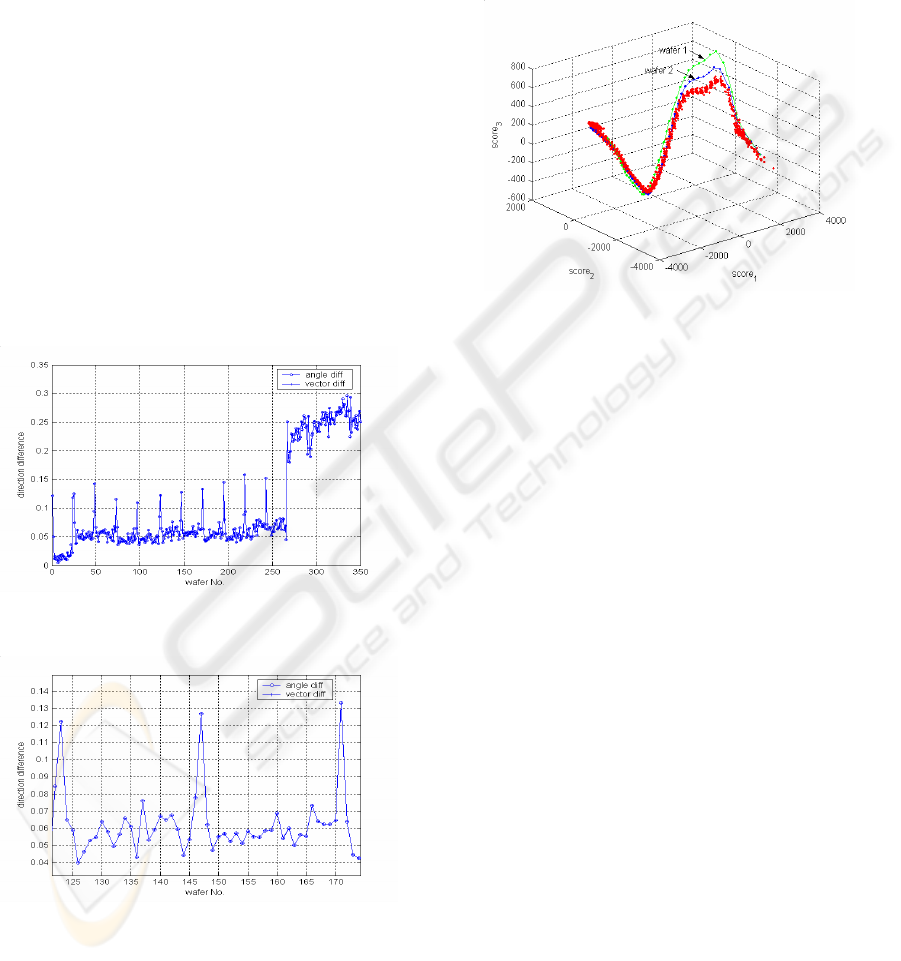
3.3 Wafer-by-wafer Analysis
Here, we simply perform PCA analysis on
individual wafer OES data sets and compare the
patterns across wafers. This allows us to explore the
variation that takes place within lots.
Fig. 7 shows the variation in wafer-PC
1
direction
over all the wafers with lot-PC
1
from lot 1 taken as a
reference. The plasma change at lot 12 observed in
the lot-PC analysis is clearly present in this data as
well, as is a small offset during the first lot.
Large spikes are evident throughout Fig. 7.
These occur at the first wafer in each lot. This is
highlighted in Fig. 8 which shows a zoomed in view
of Fig. 7 covering two lots. These sharp changes
were attributed to changes in the absorption
characteristics of the plasma chamber wall as a
result of a cleaning cycle that is performed between
lots. While a dummy etch cycle is performed
following each clean cycle to counter this affect, it is
clear from Fig. 8 that cleaning still has a significant
impact on plasma characteristics for the first (and to
a lesser extent) the second wafer etch of each lot.
Figure 7: Variation in wafer-PC
1
direction across all
wafers (using lot-PC
1
from lot 1 as a reference).
Figure 8: Variation in wafer-PC
1
direction over two lots.
3.4 Score Patterns
As an illustration of the data compression and
pattern visualisation capabilities of PCA the score
patterns generated by the OES data for all the wafers
in lot 9 are plotted in Fig. 9. Here, the first three lot-
PC loadings from lot 8 were used as a reference PC
model and the PC-scores for each wafer calculated
according to Eq. (4). It is easy to see that the
evolution of the OES data for the first and second
wafers is substantially different from the remaining
wafers, as predicted by the wafer-PC loading
analysis.
Figure 9: The first three scores of all the wafers in lot 9.
4 CONCLUSIONS
In this paper we have demonstrated how monitoring
changes in PC directions can be a useful tool in
revealing patterns contained in the high dimensional
data sets generated from OES analysis of wafer etch
plasma chambers.
ACKNOWLEDGEMENTS
The financial support provided by Enterprise Ireland
is gratefully acknowledged.
REFERENCES
Sugawara, M., 1998. Plasma Etching: Fundamentals and
applications, Oxford University Press, New York.
Splichal, M., Anderson, H., 1987. Application of
Chemometrics to Optical Emission Spectroscopy for
Plasma Monitoring. Proc. SPIE, 2, pp. 189-203.
Jackson, J. E., 1991. A User’s Guide to Principal
Components, Wiley Interscience Press, New York.
Geladi, P., Kowalski, R. B., 1986. Partial least-squares
regression: a tutorial. Analytica Chimica. Acta., 185,
pp.1-17.
Wold, S., Geladi, P., Esbensen, K., Ohman, J., 1987.
Multi-way principal components and PLS analysis.
Journal of Chemometrics, 1, pp. 41-56.
ICINCO 2007 - International Conference on Informatics in Control, Automation and Robotics
364
