
Nanosphere Photolithography: The Influence of Nanopore Arrays
Disorder on Extraordinary Optical Transmission
Andrei Ushkov
1,2 a
, Olivier Dellea
3
, Isabelle Verrier
1
, Thomas Kampfe
1
, Alexey Shcherbakov
4 b
,
Jean-Yves Michalon
1
and Yves Jourlin
1 c
1
Univ. Lyon, UJM-Saint-Etienne, CNRS, Institut d’Optique Graduate School, Laboratoire Hubert Curien UMR 5516,
F-42023 Saint-Etienne, France
2
Center for Photonics and 2D Materials, Moscow Institute of Physics and Technology, 9 Institutsky Lane, Dolgoprudny
141700, Russia
3
Grenoble Alpes Univ., CEA-Liten, 17 rue des Martyrs, 38054 Grenoble, France
4
Department of Physics and Engineering, ITMO University, 49 Kronverksky Pr., 197101 St. Petersburg, Russia
Keywords:
Nanosphere Photolithohraphy, NPL, Extraordinary Optical Transmission, EOT, Disorder, Nanopore Array,
Diffraction Graing, Plasmonics, Numerical Simulations.
Abstract:
We analyze both experimentally and numerically the influence of nanopore arrays disorder on extraordinary
optical transmission in samples, fabricated via nanosphere photolithography. Two measures of disorder are
considered, the correlations between them are discussed using experimental and numerical data. We propose
a theoretical model which takes explicitly the disorder into account, and show how the concurrence between
nanopore depth and disorder level defines the quality of EOT excitation. Simulated spectra are in a good
agreement with experimental ones. Our results reveal the possibilities of NPL for EOT-based applications and
pave the way toward plasmonic devices with a polycrystalline design.
1 INTRODUCTION
Since its discovery in 1998 by Ebbessen (Ebbesen
et al., 1998), the Extraordinary Optical Transmission
(EOT) has been studied intensively for numerous ap-
plications in optical filtering (Wen et al., 2019), sens-
ing (Yeh et al., 2011) and energy transfer (Andrew
and Barnes, 2004). Different EOT-compatible sam-
ple designs were considered, for example continuous
or perforated thin metal films (Ushkov et al., 2019;
Jourlin et al., 2009; Sauvage-Vincent et al., 2013;
Wen et al., 2019; Park et al., 2020; Yue et al., 2014),
metallic slit arrays (Deng et al., 2018), deep undu-
lations for localized plasmon excitations (Genet and
Ebbesen, 2010). In order to fabricate samples and
study the EOT experimentally, various surface nanos-
tructuration approaches exist: Electron-Beam Lithog-
raphy (Li et al., 2010; Yue et al., 2014), Focused
Ion Beam Milling (Ebbesen et al., 1998; Hahn et al.,
2020; Liu et al., 2020b), Soft-Nanoimprinting (Cam-
a
https://orcid.org/0000-0001-8962-1599
b
https://orcid.org/0000-0002-9070-5439
c
https://orcid.org/0000-0002-7935-2150
pos et al., 2008) or Laser Interference Lithography
(Ushkov et al., 2020; Cao et al., 2018).
Nowadays the self-assembled colloidal mono-
layers attract more and more attention for practi-
cal plasmonic applications. Despite the polycrys-
talline geometry, structures fabricated via colloidal
self-assembly can support resonant optical effects.
Plasmon-mediated resonant transmission was ob-
served, for example, in samples prepared via metal
deposition into the intersticies between colloidal par-
ticles (Liu et al., 2020a; Jamiolkowski et al., 2019), or
in continuous metal films covering a self-assembled
nanosphere mask (Farcau, 2019; Quint and Pacholski,
2014; Zhang et al., 2012) with or without the removal
of particles.
The deposition of close-packed self-assembled
colloidal monolayers on different substrates is per-
formed by various modifications of the Langmuir-
Blodgett technique (Ruan et al., 2007; Dell
´
ea et al.,
2014; Lotito and Zambelli, 2016; Vogel et al.,
2011). In comparison with conventional periodic
structuration methods these approaches possess a
high throughput, are well adapted for the curved and
non-conventional surfaces (Berthod et al., 2017; Pen-
46
Ushkov, A., Dellea, O., Verrier, I., Kampfe, T., Shcherbakov, A., Michalon, J. and Jourlin, Y.
Nanosphere Photolithography: The Influence of Nanopore Arrays Disorder on Extraordinary Optical Transmission.
DOI: 10.5220/0010344400460053
In Proceedings of the 9th International Conference on Photonics, Optics and Laser Technology (PHOTOPTICS 2021), pages 46-53
ISBN: 978-989-758-492-3
Copyright
c
2021 by SCITEPRESS – Science and Technology Publications, Lda. All rights reserved
dergraph et al., 2013; Bhawalkar et al., 2010) and can
be integrated into industrial production lines (Dell
´
ea
et al., 2014).
The disorder should be explicitly taken into ac-
count for the polycrystalline structures. It was shown
both numerically and experimentally (Quint and Pa-
cholski, 2014) that the disorder in thin gold film un-
dulations flattens and lowers the optical transmission;
the randomness in film perforation positions leads to
a broadband absorption (Fang et al., 2015), polycrys-
talline structures were used as light absorbers (Qu and
Kinzel, 2016).
In this work we study the influence of disorder
on EOT in samples, prepared via an advanced sur-
face nanostructuring method called Nanosphere Pho-
tolithography (NPL) (Zhang et al., 2016). In con-
trast to other colloidal-based approaches mentioned
above, NPL is much more flexible in the nanotopogra-
phy as it employs photonic nanojets for drawing sur-
face motifs. This feature makes it possible to control
the surface undulations depth, avoid the photoresist
layer perforations and produce nanopores - the ge-
ometry more flexible for the tuning of plasmonic re-
sponse in comparison with nanoholes (Gartia et al.,
2013; Wang et al., 2013). We consider two measures
of nanopore arrays disorder, compare them and show
how to explicitly take the disorder into account in
numerical simulations. Experimental EOT measure-
ments are in a good correspondence with calculated
spectra. In addition, we propose a phenomenological
model, adapted from the 1D case (Nau et al., 2007),
for EOT calculations in disordered 2D structures. Our
results are promising to reveal the possibilities of NPL
for EOT-based applications and pave the way toward
plasmonic devices with a polycrystalline design.
2 FABRICATION AND
CHARACTERIZATION OF
SAMPLES
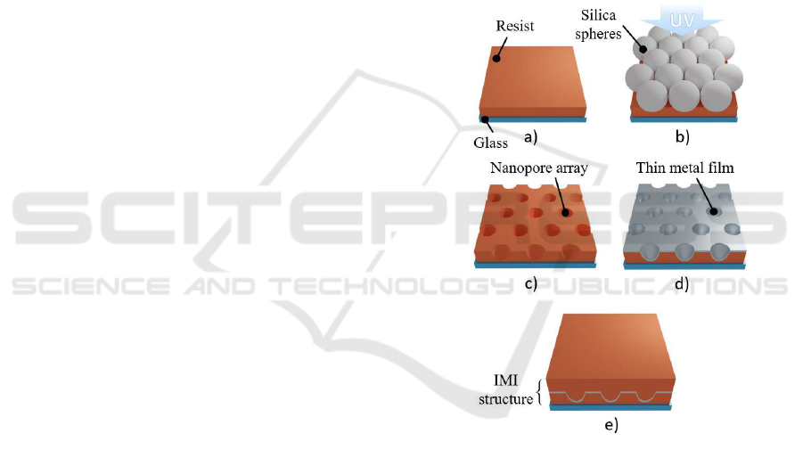
In Fig. 1 we present the main technological steps for
samples fabrication. On a surface of BK7 glass slides
3.7 × 2.5 cm, cleaned in ultrasonic acetone, ethanol
baths and DI-water bath, a 600 nm/250 nm-thick
Shipley S1805 photoresist layer is spin-coated for
1.1 µm/300 nm microsphere diameter, respectively,
see Fig. 1a. The resist was soft-baked at 60
◦
C
for 1 min. The Boostream process, developed in
CEA-Liten (Dell
´
ea et al., 2014), performs the self-
assembly of silica nano/micro particles with diam-
eters of σ
0
=1.1 µm or 300 nm into close-packed
monolayers on the water surface. The Boostream
process allows the transfer of these polycrystalline
monolayers onto the substrate in a continuous man-
ner, which is advantageous for industrial needs (Shav-
dina et al., 2015). The colloidal mask on the resist
surface acts as a microlens array for UV irradiation
(see Fig. 1b) and exposes the resist during a cer-
tain time t
exp
∼ 10 s. The exposed sample is then
cleaned in an ultrasonic bath from the colloidal parti-
cles and is developed in MF-319 developer at 8
◦
C for
t
dev
∼ 4 s. As a result, nanopore arrays appear in the
resist, see Fig. 1c. Final fabrication steps (Figs. 1d-e)
are 20 nm-thick aluminum layer deposition via mag-
netron sputtering, and the second 600 nm-thick resist
coating to protect the metal and create the symmet-
rical ”Insulator-Metal-Insulator” (IMI) structure with
improved EOT behavior.
Figure 1: Nanopore array fabrication: a) The glass slide
cleaning and a deposition of a photoresist film; b) deposi-
tion of colloidal monolayer, UV irradiation; c) the removla
of colloidal particles, resist development and formation of
nanopores; d) surface metallization; e) second resist film
deposition for the symmetrical ”Insulator-Metal-Insulator”
(IMI) structure.
An optical microscope and SEM were used to
visualize arrays with interpore distances 1.1 µm and
300 nm, respectively, before the final resist coating in
Fig. 1e. Four samples S1-S4 were fabricated experi-
mentally with different interpore distances and disor-
der, see Figs. 2a-d. Nanopore depth was measured us-
ing AFM, transmission spectra of IMI structures were
measured using the UV/Vis/NIR spectrophotometer
Cary 5000.
Nanosphere Photolithography: The Influence of Nanopore Arrays Disorder on Extraordinary Optical Transmission
47
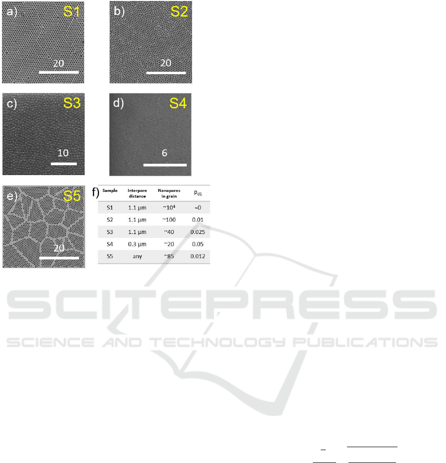
Figure 2: a)-c) Optical microscope photographs of NPL-
fabricated nanopore arrays samples S1-S3 with different
quality and a mean interpore distance σ
0
=1.1 µm. AFM-
measured nanopore depth is ∼ 220 nm; d) SEM photo-
graph of nanopore sample S4 with a mean interpore distance
σ
0
= 300 nm, AFM-measured nanopore depth 50 nm; e)
Example of simulated polycrystalline sample; f) the mean
interpore distance σ
0
, average number N of nanopores in
grains and a measure of disorder 1/N for every sample S1-
S5. Values above the scale bars in a)-e) show the distances
in microns.
3 PARAMETERS OF DISORDER
In two-dimensional systems a number of param-
eter have been proposed to quantify the disor-
der: nanopore concentration and hole-to-hole spacing
(Reilly III et al., 2010), impurity concentration (Gray
et al., 2015), statistical control parameter (Richter
et al., 2011). In this work we consider two measures
of disorder p
d1
and p
d2
: nanopores per grain and the
normalized width of the structure factor peak, respec-
tively. In what follows these parameters are used for
EOT calculations, and the correlation between them
is discussed.
Numerical simulations of transmission spectra
were performed using a proprietary GSMCC code
(Shcherbakov and Tishchenko, 2017) and the Lumer-
ical FDTD software. In the FDTD method nanopores
have vertical walls, in the GSMCC simulations the
walls were slightly slanted. Both methods produced
similar spectra, which assures the attained numerical
results. The material dispersion is used for simula-
tions, the dispersion of the resist S1805 was measured
by ellipsometry.
3.1 Nanopores Per Grain
In the context of polycrystalline geometries a natu-
ral measure of disorder is an average number N of
nanopores per grain, because this value is dimension-
less, allows to compare samples with different char-
acteristic lengths and is easy to estimate from experi-
mental data. We use the inverse number of nanopores
per grain as the first of two parameters of disorder:
p
d1
≡ 1/N. The values p
d1
for the samples S1-S4,
which are specified in Fig. 2f, confirm the visual im-
pression that the disorder increases from S1 to S4.
In order to clarify the nanopore distribution in high-
quality samples, we performed the image-processing-
based statistical analysis of large 227 µm×170 µm mi-
croscope photographs, nanopore grains with differ-
ent orientations of hexagonal lattice are depicted by
different colors in Fig. 5b. These photographs al-
low estimating an average huge number of nanopores
per grain as ∼ 10
4
by defining the grain size in S1
as 100 µm. This grain size, however, is still much
smaller than the spectrophotometer incident light spot
1 mm×3 mm, so in all samples S1-S4 it measures
a collective response of numerous randomly oriented
domains.
Figures 3a-b show the measured transmission
spectra at normal incidence through metallized sam-
ples S3 and S1, respectively. The pronounced EOT
peak exists in S1 only due to its long-range order;
the EOT resonant wavelength λ
EOT
≈ 1530 nm can
be estimated via the formula for hexagonal lattice
(Eks¸io
˘
glu et al., 2016):
λ
EOT
=
√
3σ
0
2
s
ε
d
·Re(ε
m
)
ε
d
+ Re(ε
m
)
, (1)
for 6 symmetrical first diffraction orders (m,n) =
(±1,0),(0,±1),(±1,∓1); ε
d
and ε
m
are dielectric
permittivities of dielectric and metallic layers, respec-
tively, and σ
0
is the interpore distance defined by the
diameter of the self-assembled particles. Although in
Fig. 3b the modeling of ideal hexagonal lattice is
enough for a good correspondence with experiment,
the disorder in Fig. 3a necessiates the simulation of
the periodical super cell, as shown in Fig. 3a inset.
The nanopore distribution from experimental data
was used in Fig. 3a, the cell size is adapted to include
the mean number of nanopores per grain N = 43 in
PHOTOPTICS 2021 - 9th International Conference on Photonics, Optics and Laser Technology
48
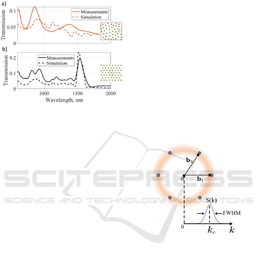
Figure 3: Transmission spectra at normal incidence with
and without EOT through samples with a mean interpore
distance 1.1 µm. Solid curves in a) and b) correspond to the
measured transmission through samples S3 and S1, respec-
tively. Dashed lines in a) and b) are the calculated spectra
of nanopore arrays arranged in periodical cells, shown as in-
sets in a) and b); red rectangles denote periodical boundary
conditions, its size in a) is 6816 × 5636 nm.
correspondence with values of Fig. 2f. Both experi-
mental and numerical results show that a high disor-
der in nanopore arrays effectively suppresses the EOT
peak.
Although the parameter p
d1
is easy to estimate
from experimental data and allows to define properly
the size of super cells with disorder, it is a geometri-
cal value which is not directly connected with sample
diffraction properties. We believe that for EOT-based
devices another parameter of disorder is more appro-
priate, introduced in the next section.
3.2 Normalized Width of the Structure
Factor Peak
As it was mentioned above, the experimental samples
consist of a huge number of randomly oriented grains,
illuminated by normally incident light during spec-
tral measurements. We study the EOT caused by first
diffraction orders; in polycrystalline samples these
orders, coming from different grains, create a circle
in reciprocal space with the radius k
c
≡
|
b
1
|
=
|
b
2
|
,
where b
1
and b
2
are basis reciprocal vectors for an
ideal hexagonal grating, see Fig. 4. To calculate
a Fourier transform ρ
k
of nanopore arrays we use a
set of two-dimensional Dirac delta functions ρ(r) =
∑
N
i=1
δ(r −r
i
), which are zero except nanopore cen-
ters r = r
i
, and get ρ
k
=
∑
N
i=1
exp(ik ·r
i
). The
blue profile in Fig. 4 represents the radial-averaged
static structure factor S(k), which is proportional to
the squared modulus of Fourier amplitudes: S(k) =
hρ
k
ρ
−k
i/N.
If nanopore grains are large enough (as for the
sample S1), the circle is thin, and the measured EOT
is almost the same as for ideal hexagonal grating
(see Fig. 3b), even if the total number of illumi-
nated grains is big. The transmission through peri-
odical hexagonal lattices weakly depends to incident
light polarization due to the 6-fold rotational symme-
try (Zhao et al., 2017). Our preliminary calculations
show that transmission variations are well below 1%
for any linear polarization in hexagonally arranged
nanopores. For samples with smaller grains the recip-
rocal space circle is wider in analogy with diffraction
in amorphous liquids (Ziman, 1979; Rojas-Ochoa
et al., 2004). Consequently, the Full Width at Half
Maximum (FWHM) of the radial distribution can
serve as a measure of disorder, connected with the
structure diffraction properties. In this paper we con-
sider the dimensionless parameter of disorder p
d2
≡
FWHM/k
c
.
Figure 4: Sketch of the first Fourier harmonics circle for
polycrystalline gratings. Reciprocal basis vectors b
1
and b
2
and 6 first diffraction orders denoted by blue points are de-
fined by ideal hexagonal nanopore arrangement. The profile
along the circles radius (in blue) represents the static struc-
ture factor S(k).
The both parameters p
d1
and p
d2
grow with the
growth of disorder, their values for experimental sam-
ples S1-S4 are shown in Fig. 5a. According to
this figure, the reciprocal space circle slows its width
growth with the increase of p
d1
, it means that diffrac-
tion properties of structures with small crystallites do
not depend sufficiently on the disorder level, in con-
trast to samples with large crystallites and a long-
range order. In order to understand this behavior bet-
ter we developed a simple model of polycrystalline
nanopore arrays (see, for example, S5 in Fig. 2e).
For every simulation a set of points is chosen ran-
domly, and the Voronoi diagram of this set defines
Nanosphere Photolithography: The Influence of Nanopore Arrays Disorder on Extraordinary Optical Transmission
49
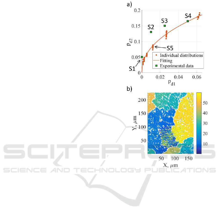
the nanopore grains boundaries. The space inside
grains is filled with hexagonally arranged elements
(nanopores), the lattice orientation is chosen ran-
domly in every grain. We leave the thin stripes along
boundaries empty to avoid the overlap of nanopores
from different grains. In such a way, numerous re-
alizations of nanopore arrays with different p
d1
were
simulated, and corresponding values of p
d2
were cal-
culated. In Fig. 5a parameters p
d1
and p
d2
of indi-
vidual simulated nanopore distributions are denoted,
together with a phenomenological power function fit-
ting p
d2
(p
d1
) = 0.63p
0.45
d1
.
The comparison of experimental and modeled de-
pendences p
d2
(p
d1
) in Fig. 5a allows to make two
observations. Firstly, the modeled monotone func-
tion generally repeats the experimental behavior, thus
the average number of nanopores per grain can, to
a first approximation, determine a diffraction qual-
ity of samples. Secondly, the experimental values of
p
d2
tend to be larger than those predicted by a sim-
ple polycrystalline model. It can be explained by
the presence of additional defects in nanopore arrays
along with randomly oriented crystallites, i.e. hexag-
onal lattice phase jumps (Avrutsky et al., 2000) (white
uncolored lines in Fig. 5b) and regions between
grains, filled with randomly distributed nanopores.
Although these defects can be introduced into the
modelling, it goes beyond the scope of this paper. In
the following section we use the ”diffraction” param-
eter of disorder for numerical simulation of EOT.
3.3 Influence of Nanopore Arrays
Disorder on EOT
In order to utilize the parameter p
d2
and introduce
explicitly the disorder into numerical EOT calcula-
tions we propose a model, adapted from the 1D case
(Nau et al., 2007). A radial-symmetric structure fac-
tor S(k), calculated for experimental nanopore distri-
bution, is least square fitted to a Gaussian to obtain
the value of p
d2
. At the same time, the structure peak
width defines a set of effective first diffraction orders
k, which come from different grains and give a con-
tribution α
k
T
k
(λ) to the total transmission T(λ) at a
wavelength λ. We assume a simple incoherent sum-
mation of these partial contributions because of nu-
merous randomly oriented and distributed grains. The
scaling factor α
k
depends on the density of excited
modes and is proportional to the corresponding value
S(k).
The total transmission is the sum of all par-
tial contributions with k around the structure factor
peak, where the α
k
is sufficiently non-zero: T(λ) =
∑
k
α
k
T
k
(λ). Partial spectra T
k
are obtained from the
Figure 5: a) Correlation between two disorder parameters
p
d1
and p
d2
for simulated (brown points and fitting line) and
experimental nanopore distributions (green squares). Sam-
ples S1-S4 and the example of simulated distribution S5 are
shown in Figs. 2a-e. The phenomenological power function
fitting p
d2
= 0.63p
0.45
d1
is used.
simulation of perfect samples (Nau et al., 2007).
Figure 6a shows several calculated transmission
spectra at normal incidence for 50 nm-depth nanopore
arrays, for different disorder levels p
d2
. The ex-
perimentally measured value of EOT and its spec-
tral shape for sample S4 is in a good agreement
with theoretical results at appropriate disorder level,
compare with its value in Fig. 5a. The ”diffrac-
tion” parameter p
d2
is convenient to study the influ-
ence of continuously varying disorder on EOT. Fig-
ure 6b demonstrates the change of maximum EOT
value with nanopore depth at numerous disorder lev-
els. Generally, the disorder suppresses the resonant
transmission. Interestingly, it can also turn a trans-
mission decreasing with a depth growth into an in-
creasing one, for deep gratings (see the highest and
the lowest curves in Fig. 6b at depth>100 nm). The
3D-representation of calculated data in Fig. 6c re-
PHOTOPTICS 2021 - 9th International Conference on Photonics, Optics and Laser Technology
50
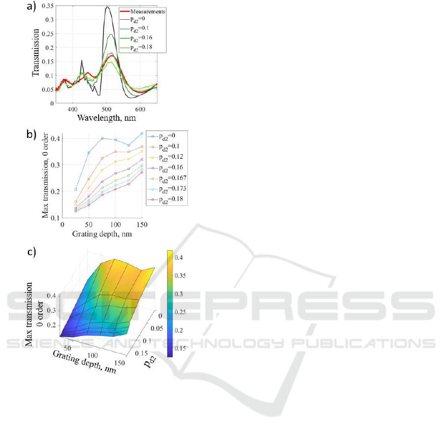
Figure 6: a) A set of calculated transmission spectra (tones
of green) at normal incidence with different parameter of
disorder p
d2
. A red curve shows an experimentally mea-
sured transmission for the sample S4. Simulated and exper-
imental nanopore depth is 50 nm; b) calculated maximum
EOT transmission as a function of graing depth for a set of
p
d2
; c) 3D-representation of data from b), showing a con-
currence between grating depth and disorder for the value
of EOT.
veals an interplay between grating depth and disorder
for establishing a EOT value.
4 CONCLUSIONS
In conclusion, we analyzed both experimentally and
numerically the influence of nanopore arrays disor-
der on extraordinary optical transmission in samples,
fabricated via nanosphere photolithography. We used
two measures of disorder: ”geometrical” parameter
p
d1
and ”diffraction” parameter p
d2
, and constructed a
simple model of nanopore distributions to understand
better the correlations between p
d1
and p
d2
. We con-
sider the value of p
d2
as a more appropriate and con-
venient one for numerical simulation of disordered
samples in the context of EOT, and proposed a theo-
retical model which takes explicitly the disorder into
account. Simulated spectra are in a good agreement
with experimental ones. We have shown how the con-
currence between nanopore depth and disorder level
defines the quality of EOT excitation. We believe
that our results, which reveal the possibilities of NPL
for EOT-based applications, will pave the way toward
plasmonic devices with a polycrystalline design.
ACKNOWLEDGEMENTS
The work was funded by the SIS 488 doctoral school
of Saint-Etienne, university of Lyon (France), and
by RFBR, project number 19-32-90034. The au-
thors would like to thank CNRS engineers Marion
HOCHEDEL and Arnaud VALOUR for the technical
support.
REFERENCES
Andrew, P. and Barnes, W. (2004). Energy transfer across
a metal film mediated by surface plasmon polaritons.
Science, 306(5698):1002–1005.
Avrutsky, I., Li, B., and Zhao, Y. (2000). Characterization
of two-dimensional colloidal polycrystalline materials
using optical diffraction. JOSA B, 17(6):904–909.
Berthod, L., Shavdina, O., Vocanson, F., Langlet, M., Del-
lea, O., Veillas, C., Reynaud, S., Verrier, I., and
Jourlin, Y. (2017). Colloidal photolithography applied
to functional microstructure on cylinder based on pho-
topatternable TiO
2
sol-gel. Microelectronic Engineer-
ing, 177:46–51.
Bhawalkar, S. P., Qian, J., Heiber, M. C., and Jia, L.
(2010). Development of a colloidal lithography
method for patterning nonplanar surfaces. Langmuir,
26(22):16662–16666.
Campos, L. M., Meinel, I., Guino, R. G., Schierhorn, M.,
Gupta, N., Stucky, G. D., and Hawker, C. J. (2008).
Highly versatile and robust materials for soft imprint
lithography based on thiol-ene click chemistry. Ad-
vanced Materials, 20(19):3728–3733.
Cao, J., Sun, Y., Zhu, H., Cao, M., Zhang, X., and Gao,
S. (2018). Plasmon-enhanced optical transmission at
multiple wavelengths through an asymmetric corru-
gated thin silver film. Plasmonics, 13(5):1549–1554.
Dell
´
ea, O., Shavdina, O., Fugier, P., Coronel, P., Ollier, E.,
and D
´
esage, S.-F. (2014). Control methods in micro-
spheres precision assembly for colloidal lithography.
Nanosphere Photolithography: The Influence of Nanopore Arrays Disorder on Extraordinary Optical Transmission
51

In Ratchev, S., editor, Precision Assembly Technolo-
gies and Systems, pages 107–117. Springer Heidel-
berg.
Deng, Z.-L., Cao, Y., Li, X., and Wang, G. P. (2018). Mul-
tifunctional metasurface: from extraordinary optical
transmission to extraordinary optical diffraction in a
single structure. Photonics Research, 6(5):443–450.
Ebbesen, T. W., Lezec, H. J., Ghaemi, H., Thio, T., and
Wolff, P. A. (1998). Extraordinary optical transmis-
sion through sub-wavelength hole arrays. Nature,
391(6668):667–669.
Eks¸io
˘
glu, Y., Cetin, A. E., and Petr
´
a
ˇ
cek, J. (2016). Opti-
cal response of plasmonic nanohole arrays: compar-
ison of square and hexagonal lattices. Plasmonics,
11(3):851–856.
Fang, X., Lou, M., Bao, H., and Zhao, C. (2015). Thin films
with disordered nanohole patterns for solar radiation
absorbers. Journal of Quantitative Spectroscopy and
Radiative Transfer, 158:145–153.
Farcau, C. (2019). Metal-coated microsphere monolayers as
surface plasmon resonance sensors operating in both
transmission and reflection modes. Scientific reports,
9(1):1–9.
Gartia, M. R., Hsiao, A., Pokhriyal, A., Seo, S., Kulsharova,
G., Cunningham, B. T., Bond, T. C., and Liu, G. L.
(2013). Colorimetric plasmon resonance imaging us-
ing nano lycurgus cup arrays. Advanced Optical Ma-
terials, 1(1):68–76.
Genet, C. and Ebbesen, T. W. (2010). Light in tiny holes.
In Nanoscience And Technology: A Collection of Re-
views from Nature Journals, pages 205–212. World
Scientific.
Gray, A. T., Mould, E., Royall, C. P., and Williams, I.
(2015). Structural characterisation of polycrystalline
colloidal monolayers in the presence of aspherical
impurities. Journal of Physics: Condensed Matter,
27(19):194108.
Hahn, C., Hajebifard, A., and Berini, P. (2020). Helium fo-
cused ion beam direct milling of plasmonic heptamer-
arranged nanohole arrays. Nanophotonics, 9(2):393–
399.
Jamiolkowski, R. M., Chen, K. Y., Fiorenza, S. A., Tate,
A. M., Pfeil, S. H., and Goldman, Y. E. (2019).
Nanoaperture fabrication via colloidal lithography for
single molecule fluorescence analysis. PloS one,
14:10.
Jourlin, Y., Tonchev, S., Tishchenko, A., Pedri, C., Veillas,
C., Parriaux, O., Last, A., and Lacroute, Y. (2009).
Spatially and polarization resolved plasmon mediated
transmission through continuous metal films. Optics
express, 17(14):12155–12166.
Li, J.-Y., Hua, Y.-L., Fu, J.-X., and Li, Z.-Y. (2010). Influ-
ence of hole geometry and lattice constant on extraor-
dinary optical transmission through subwavelength
hole arrays in metal films. Journal of Applied Physics,
107(7):073101.
Liu, J., Zhang, X., Li, W., Jiang, C., Wang, Z., and Xiao, X.
(2020a). Recent progress in periodic patterning fabri-
cated by self-assembly of colloidal spheres for optical
applications. Sci. China Mater., 63:1418–1437.
Liu, Q., Song, Y., Zeng, P., Zhang, C., Chen, Y., Wang, H.,
Luo, Y., and Duan, H. (2020b). High-fidelity fabrica-
tion of plasmonic nanoholes array via ion-beam pla-
narization for extraordinary transmission applications.
Applied Surface Science, 526:146690.
Lotito, V. and Zambelli, T. (2016). Self-assembly of single-
sized and binary colloidal particles at air/water in-
terface by surface confinement and water discharge.
Langmuir, 32(37):9582–9590.
Nau, D., Sch
¨
onhardt, A., Bauer, C., Christ, A., Zentgraf,
T., Kuhl, J., Klein, M., and Giessen, H. (2007). Cor-
relation effects in disordered metallic photonic crystal
slabs. Physical review letters, 98(13):133902.
Park, J., Lee, H., Gliserin, A., Kim, K., and Kim, S. (2020).
Spectral shifting in extraordinary optical transmission
by polarization-dependent surface plasmon coupling.
Plasmonics, 15(2):489–494.
Pendergraph, S. A., Park, J. Y., Hendricks, N. R., Crosby,
A. J., and Carter, K. R. (2013). Facile colloidal lithog-
raphy on rough and non-planar surfaces for asymmet-
ric patterning. Small, 9(18):3037–3042.
Qu, C. and Kinzel, E. C. (2016). Polycrystalline metasur-
face perfect absorbers fabricated using microsphere
photolithography. Optics letters, 41(15):3399–3402.
Quint, S. and Pacholski, C. (2014). Getting real: In-
fluence of structural disorder on the performance of
plasmonic hole array sensors fabricated by a bottom-
up approach. Journal of Materials Chemistry C,
2(36):7632–7638.
Reilly III, T. H., Tenent, R. C., Barnes, T. M., Rowlen,
K. L., and van de Lagemaat, J. (2010). Controlling the
optical properties of plasmonic disordered nanohole
silver films. ACS nano, 4(2):615–624.
Richter, C., Schmiedeberg, M., and Stark, H. (2011). A col-
loidal model system with tunable disorder: Solid-fluid
transition and discontinuities in the limit of zero dis-
order. The European Physical Journal E, 34(10):107.
Rojas-Ochoa, L. F., Mendez-Alcaraz, J., S
´
aenz, J.,
Schurtenberger, P., and Scheffold, F. (2004). Pho-
tonic properties of strongly correlated colloidal liq-
uids. Physical review letters, 93(7):073903.
Ruan, W.-d., L
¨
u, Z.-c., Nan, J., Wang, C.-x., Bing,
Z., and Zhang, J.-h. (2007). Facile fabrication of
large area polystyrene colloidal crystal monolayer via
surfactant-free langmuir-blodgett technique. Chemi-
cal Research in Chinese Universities, 23(6):712–714.
Sauvage-Vincent, J., Tonchev, S., Veillas, C., Reynaud, S.,
and Jourlin, Y. (2013). Optical security device for doc-
ument protection using plasmon resonant transmis-
sion through a thin corrugated metallic film embed-
ded in a plastic foil. Journal of the European Optical
Society-Rapid publications, 8:1–6.
Shavdina, O., Berthod, L., Kampfe, T., Reynaud, S., Veil-
las, C., Verrier, I., Langlet, M., Vocanson, F., Fugier,
P., Jourlin, Y., and Dellea, O. (2015). Large area fabri-
cation of periodic TiO
2
nanopillars using microsphere
photolithography on a photopatternable sol–gel film.
Langmuir, 31(28):7877–7884.
Shcherbakov, A. A. and Tishchenko, A. V. (2017). Gen-
eralized source method in curvilinear coordinates for
PHOTOPTICS 2021 - 9th International Conference on Photonics, Optics and Laser Technology
52

2d grating diffraction simulation. J. Quant. Spectrosc.
Radiat. Transf., 187:76–96.
Ushkov, A., Verrier, I., Kampfe, T., and Jourlin, Y. (2020).
Subwavelength diffraction gratings with macroscopic
moir
´
e patterns generated via laser interference lithog-
raphy. Optics Express, 28(11):16453–16468.
Ushkov, A. A., Shcherbakov, A. A., Verrier, I., Kampfe,
T., and Jourlin, Y. (2019). Systematic study of res-
onant transmission effects in visible band using vari-
able depth gratings. Scientific reports, 9(1):1–9.
Vogel, N., de Viguerie, L., Jonas, U., Weiss, C. K.,
and Landfester, K. (2011). Wafer-scale fabrica-
tion of ordered binary colloidal monolayers with ad-
justable stoichiometries. Advanced functional materi-
als, 21(16):3064–3073.
Wang, W., Peng, Y., and Cui, T. (2013). Simulation study
of extraordinary optical transmission induced by sub-
wavelength nanopore arrays towards label-free bio-
chemical analysis. In 2013 International Conference
on Manipulation, Manufacturing and Measurement
on the Nanoscale, pages 140–145. IEEE.
Wen, K., Luo, X.-Q., Chen, Z., Zhu, W., Guo, W., and
Wang, X. (2019). Enhanced optical transmission as-
sisted near-infrared plasmonic optical filter via hybrid
subwavelength structures. Plasmonics, 14(6):1649–
1657.
Yeh, W.-H., Petefish, J. W., and Hillier, A. C. (2011).
Diffraction-based tracking of surface plasmon reso-
nance enhanced transmission through a gold-coated
grating. Analytical chemistry, 83(15):6047–6053.
Yue, W., Wang, Z., Yang, Y., Li, J., Wu, Y., Chen, L., Ooi,
B., Wang, X., and Zhang, X.-x. (2014). Enhanced ex-
traordinary optical transmission (EOT) through arrays
of bridged nanohole pairs and their sensing applica-
tions. Nanoscale, 6(14):7917–7923.
Zhang, X., Li, Z., Ye, S., Wu, S., Zhang, J., Cui, L., Li,
A., Wang, T., Li, S., and Yang, B. (2012). Elevated
ag nanohole arrays for high performance plasmonic
sensors based on extraordinary optical transmission.
Journal of Materials Chemistry, 22(18):8903–8910.
Zhang, Z., Geng, C., Hao, Z., Wei, T., and Yan, Q. (2016).
Recent advancement on micro-/nano-spherical lens
photolithography based on monolayer colloidal crys-
tals. Advances in colloid and interface science,
228:105–122.
Zhao, J., Yu, X., Yang, X., Xiang, Q., Duan, H., and
Yu, Y. (2017). Polarization independent subtractive
color printing based on ultrathin hexagonal nanodisk-
nanohole hybrid structure arrays. Optics express,
25(19):23137–23145.
Ziman, J. M. (1979). Models of disorder: the theoretical
physics of homogeneously disordered systems. Cam-
bridge University.
Nanosphere Photolithography: The Influence of Nanopore Arrays Disorder on Extraordinary Optical Transmission
53
