
Junction Temperature Measurement
in Optically-Controlled Power Mosfet
Sandro Rao
1
, Elisa D. Mallemace
1
, G. Cocorullo
2
, L. Dehimi
3,4
and Francesco G. Della Corte
1
1
Department of Information Engineering Infrastructures and Sustainable Energy (DIIES), Università Mediterranea,
89122, Reggio Calabria, Italy
2
Dipartimento di Ingegneria Informatica, Modellistica, Elettronica e Sistemistica (DIMES), Università della Calabria,
87036, Rende, Cosenza, Italy
3
Laboratory of Metallic and Semi-conducting Materials (LMSM), University of Biskra, BP 145, 07000 Biskra, Algeria
4
Faculty of Material Science, University of Batna, 05000 Batna, Algeria
Keywords: Optically-Controlled SiC Power MOSFET, Temperature Monitoring, Integrated-Fabry-Perot Cavity, Junction
Temperature.
Abstract: The temperature-dependent optical properties of silicon carbide (SiC), such as refractive index and
reflectivity, have been used for a direct monitoring of the junction temperature of a power MOSFET. In
particular, the optical response of a 4H-SiC MOSFET-integrated Fabry-Perot cavity to temperature changes
has been investigated through parametric optical simulations at the wavelength of 450 nm. The reflected
optical power exhibited oscillatory patterns caused by the multiple beam interference for which the MOSFET
epilayer, between the gate-oxide and the doped 4H-SiC substrate, acts as a Fabry-Perot etalon. These results
were used to calculate the refractive index change and, therefore, the optical phase shift of ∆φ= π/2
corresponding to a temperature variation that can be considered as a warning for the device “health”. In
practical applications, the periodic monitoring of the optic spectrum at the interferometric structure output
gives an essential information about the device operating temperature condition that, for high power
operations, may lead to device damages or system failure.
1 INTRODUCTION
The thermal control of any semiconductor device is
of extreme importance to achieve optimal
performance, reliability and durability. Temperature
has a strong influence on the main electrical
parameters and, for power devices or more complex
electronic modules, in particular, a thermal
management during the operating lifetime is
exploited as a damage indicator to prevent the system
failure.
In general, the thermal resistance of a device, R
T
,
is given by: R
T
=ΔT/P,
where ΔT is the rise in
temperature with respect to a specified reference
point, and P is the power dissipated by the device.
Ideally, the thermal resistance is a device
specification that permits the user to determine the
maximum temperature for any power level. In order
for a device manufacturer to specify and, for a user to
verify R
T
, an accurate, reliable method for measuring
the device internal temperature is required
(Blackburn & Berning, 1982).
The technology of silicon carbide (SiC) is today
recognized to be one of the most practical for pulsed-
power applications taking, moreover, advantage from
the high thermal conductivity of SiC which lowers the
thermal resistance for a given active area and current
density (Mazumder & Sarkar, 2009; Della Corte,
Giglio, Pangallo, & Rao, 2018).
4H-SiC-based switching devices, in particular,
can operate at high voltages and high currents up to
theoretical temperatures higher than 800°C
(Neudeck, 2006), however, the maximum allowed
operating temperature of commercialized SiC-
MOSFETs is usually lower than 175°C, limited by
metals contacts, passivating materials and packaging
technology (CREE, 2019).
Therefore, a continuous monitoring of the device
junction temperature (T
j
), with a minimum of
interference from the other device parameters, is
110
Rao, S., Mallemace, E., Cocorullo, G., Dehimi, L. and Della Corte, F.
Junction Temperature Measurement in Optically-Controlled Power Mosfet.
DOI: 10.5220/0010327001100114
In Proceedings of the 9th International Conference on Photonics, Optics and Laser Technology (PHOTOPTICS 2021), pages 110-114
ISBN: 978-989-758-492-3
Copyright
c
2021 by SCITEPRESS – Science and Technology Publications, Lda. All rights reserved

essential to verify the power device “health” and to
prevent damages.
In literature, many methods have been proposed
for monitoring the power MOSFET temperature;
these can be divided in three main categories
(Blackburn, 2004): optical, physical contact and
electrical methods. The main solutions use
luminescence (Schuermeyer et al., 2000), Raman
spectroscopy (Kuball et al., 2002), liquid crystals
thermographic (Parsley, 1991), turn-on delay of
impulse signal (Shi et al., 2017)
or an external
temperature sensor (Rao, Pangallo, & Della Corte,
2015).
However, each of these approaches only provide
a global temperature whose value differs greatly from
the real device junction temperature, T
j
.
Recently, the linear relation between the body-
drain voltage of power MOSFETs and their junction
temperature has been experimentally investigated by
these authors in a wide range of bias currents in a
temperature range from about 22 up 150 °C
(Pangallo, Rao, Adinolfi, Graditi, & Della Corte,
2019). Moreover, a new method for measuring the T
j
of power light emitting diodes (LEDs), used for
lighting, has been presented (Pangallo et al., 2018)
together with a microcontroller-based circuit
designed and realized for a real-time monitoring
(Della Corte et al., 2020).
In this work, we present a new approach allowing
the junction temperature control of a 4H-SiC power
MOSFET through an optical signal. Optical
simulation results of the MOSFET-integrated Fabry-
Perot cavity, consisting of the gate oxide, the epilayer
and the doped substrate, show that the temperature-
induced refractive index change allows to calculate
the T
j
variation. The proposed optically-controlled
power MOSFET junction temperature can be done
during the lifetime of the device in order to alert the
user before its failure.
2 DEVICE STRUCTURE AND
SIMULATION RESULTS
A 4H-SiC-based MOSFET structure has been
modeled using R-Soft CAD (RSoft, 2006), a photonic
device simulator using the beam propagation method,
to perform 3-D parametric optical simulations.
The MOSFET-integrated Fabry-Perot cavity, in
the <x,z> plane, where <z> is the optical propagation
direction, is shown in Figure 1. Simulations were
performed using a continuous laser optical beam, at
the wavelength of 450 nm, launched on top of the
gate-oxide layer. Layers thickness and optical data of
the materials used for simulations are listed in Table
1.
As shown in Figure 1, the optically-controlled
MOSFET has an optical window instead of the gate
electrode. When the light falls on it, no excess
carriers, at the considered wavelength of 450 nm, are
generated, therefore, the conductivity as well as the
drain current are not influenced by the optical signal
used for the device temperature monitoring. It is
worth noting that the control of T
j
is generally done
using a short pulse laser source with a repetition rate
comparable or lower than the slow thermal dynamics
of the device.
Figure 1: Schematic cross-section of an optically-controlled
4H-SiC MOSFET. The MOSFET-integrated FP cavity
consists of the 4H-SiC epilayer between the SiO
2
gate-oxide
and the 4H-SiC heavily-doped substrate.
Table 1: Optical and geometrical parameters of the
MOSFET-integrated FP cavity.
Silicon oxide thickness (t
ox
) [µm] 0.1
Channel length [µm] (Della Corte, De
Martino, Pezzimenti, Adinolfi, & Graditi,
2018)
6.5
Epilayer thickness (t
epi
) [µm] 10
Substrate thickness (t
sub
) [µm] 2.5
Silicon oxide refractive index (n
ox
) 1.44
Epilayer refractive index (n
epi
)
(Watanabe, Kimoto, & Suda, 2012)
2.73
Substrate refractive index (n
sub
) (Lim,
Manzur, & Kar, 2011)
2.65
From a technological point of view, the power
MOSFET fabrication requires a high quality of both
epilayer surfaces, therefore careful attention towards
the morphology of all stacked-layers is performed in
any industrial process. Optical microscopy (OM) is a
Junction Temperature Measurement in Optically-Controlled Power Mosfet
111
fast and non-destructive method, which is generally
used after each growth to determine the morphology,
uniformity and epilayer defects (Ager III, 1998).
Moreover, OM is carried out also to reveal any
presence of 4H-SiC domains when the growth is
performed on doped-SiC substrates.
Under these technological conditions, a
reflectance spectrum can be registered at the input of
the Fabry-Perot (FP) cavity consisting of the
smoothed gate-oxide/epilayer and epilayer/substrate
interfaces.
The interference fringes are detected, in case of
homoepitaxy, as in our structure, due to a difference
in refractive index between the epilayer and the
substrate (see Table 1). This difference is achieved by
the strong doping concentration discrepancy between
the 4H-SiC epilayer (N
D
-N
A
~10
16
cm
-3
) and the 4H-
SiC substrate, which has usually a nitrogen doping
concentration in the range 10
18
-10
19
cm
-3
(Della Corte
et al., 2018).
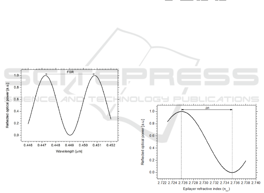
Figure 2 shows the simulated FP reflected
spectrum centered at the wavelengths of interest. The
corresponding calculated Free Spectral Range (FSR)
is 3.57 nm, in agreement with the theoretical value
(Agrawal, 2012).
Figure 2: Normalized-reflected output power vs.
wavelength. The FSR is the spacing in wavelength
calculated between two successive reflected optical
intensity maxima (or minima) of the FP cavity.
For the refractive index values considered in this
work (n
sub
=2.65, n
epi
=2.73), the modulation depth,
defined as M
%
= (I
MAX
– I
MIN
)/ I
MAX,
where I
MAX
and
I
MIN
are the maximum and minimum intensities of the
reflected signal, is 15.2%, varying from M
%
=24.2%
down to M
%
=5.4% for n
sub
=2.6 and n
sub
=2.7,
respectively.
Moreover, parametric simulations were
performed in order to verify the independence of the
gate oxide thickness, considered in this work from 50
to 500 nm, on the FP outputs. The used value of 100
nm is typical for commercial power MOSFETs.
As known, the temperature dependence of the
optical path length of a monochromatic light, incident
perpendicularly upon a device surface and traveling
through a FP cavity, is given by the product between
the refractive index of the cavity material, n, and its
length, L (Steimacher et al., 2004).
Due to the environmental and/or operating
conditions, a variation of the temperature, ΔT, induces
both n and L change and, therefore, the optical length
changes too, as well as the interference phase angle
of the oscillatory pattern, φ, as expressed by the
following equation (Mathew et al., 2015):
∆𝜑
∆𝑇
4𝜋𝑛𝐿
𝜆
1
𝑛
𝑑𝑛
𝑑𝑇
1
𝐿
𝑑𝐿
𝑑𝑇
(1)
where dn/dT and dL/dT are the thermo-optic
(TOC) (Faggio, Messina, Gnisci, Rao, & Malara,
2019) and the thermal-expansion coefficients,
respectively.
In our structure, the MOSFET-integrated FP
cavity length is the epilayer thickness, t
epi
, and the
corresponding refractive index is n
epi
. A phase shift of
Δφ=π/2 results in a complete tuning of resonance
wavelengths and, from equation 1, if we consider a
TOC of 7.8∙10
-5
at λ=450 nm (Watanabe et al., 2012),
and dL/dT = 2.2∙10
-6
(Nakabayashi, Fujimoto,
Katsuno, & Ohtani, 2006), the theoretical temperature
change is expected to be ΔT
π/2
=133.92°C.
Figure 3: Reflected output power vs. epilayer refractive
index. The difference of refractive index between a
maximum and a minimum value of the refrected power is
Δn=9.65∙10
-3
.
Figure 3 shows the parametric simulation results
of the MOSFET-integrated FP cavity spectrum where
the epilayer refractive index has been varied in a
range allowing a gradual and complete detuning of
PHOTOPTICS 2021 - 9th International Conference on Photonics, Optics and Laser Technology
112

the cavity, e.g., from a maximum to a minimum of the
reflected power at the gate-oxide output.
Assuming for 4H-SiC a TOC of 7.8∙10
-5
, it can be
calculated that a complete FP detuning is introduced
in our L=10 µm-thick 4H-SiC epitaxial layer by a
thermally-induced refractive index change of
Δn=9.65∙10
-3
corresponding to a temperature
variation of ΔT
π/2
=123.7°C.
It is worth noting that this temperature variation
mainly depends on the wavelength of the optical
signal and/or on the MOSFET epilayer thickness.
However, if the optical parameters, at a specific
wavelength, as well as the MOSFET geometry, are
not known, an easy pre-characterization of the
MOSFET-integrated FP cavity spectrum allows the
determination of the temperature change (ΔT
π/2
)
required for the output optical power to move from a
maximum (or minimum) to a subsequent minimum
(or maximum).
In a practical application, if we consider, e.g., an
external temperature of T
e
=30°C, the monitoring of
the multiple-beam interference signal, from its
resonance position, gives us the power device/system
operating temperature condition (T=T
e
+ΔT) that, for
high power operations, in particular, may lead to
permanent damage or performance variations.
3 CONCLUSIONS
In this paper, a new method for real-time monitoring
the junction temperature of a SiC-based power
MOSFET has been presented.
The MOSFET epilayer between the gate-oxide
and the heavily doped substrate naturally forms an
integrated Fabry-Perot (FP) cavity that can be
exploited to calculate the temperature variation
during the power device operating life.
Simulation results, performed at the wavelength
of 450 nm, showed that a complete FP detuning is
introduced in our L=10 µm-thick 4H-SiC epitaxial
layer by a thermally-induced refractive index change
of Δn=9.65∙10
-3
corresponding to a temperature
variation of 123.7°C. The optically-controlled
junction temperature increase is essential to prevent
the device overheating.
This method can be applied in many power
applications, including signal-conditioning circuits
for sensors (Rao, Pangallo, & Della Corte, 2016), and
for wide-band materials-based switching system
control where, changes in temperature above the
temperature limit, lead to a mean time to failure
reduction or device disruption.
REFERENCES
Blackburn, D. L., & Berning, D. W. (1982, June). Power
MOSFET temperature measurements. In 1982 IEEE
Power Electronics Specialists conference (pp. 400-
407). IEEE.
Mazumder, S. K., & Sarkar, T. (2009). SiC based optically-
gated high-power solid-state switch for pulsed-power
application. In Materials Science Forum (Vol. 600, pp.
1195-1198). Trans Tech Publications Ltd.
Della Corte, F. G., Giglio, I., Pangallo, G., & Rao, S.
(2018). Electro-optical modulation in a 4H-SiC slab
induced by carrier depletion in a Schottky diode. IEEE
Photonics Technology Letters, 30(9), 877-880.
Neudeck, P. G. (2006). Silicon carbide technology. The
VLSI handbook, 20061800.
CREE. C3M0021120K Silicon Carbide Power MOSFET,
Datasheet. 2019.
Blackburn, D. L. (2004, March). Temperature
measurements of semiconductor devices-a review. In
Twentieth Annual IEEE Semiconductor Thermal
Measurement and Management Symposium (IEEE Cat.
No. 04CH37545) (pp. 70-80). IEEE.
Schuermeyer, F., Fitch, R., Dettmer, R., Gillespie, J.,
Bozada, C., Nakano, K., ... & Liou, L. L. (2000,
August). Thermal studies on heterostructure bipolar
transistors using electroluminescence. In Proceedings
2000 IEEE/Cornell Conference on High Performance
Devices (Cat. No. 00CH37122) (pp. 45-50). IEEE.
Kuball, M., Hayes, J. M., Uren, M. J., Martin, I., Birbeck,
J. C. H., Balmer, R. S., & Hughes, B. T. (2002).
Measurement of temperature in active high-power
AlGaN/GaN HFETs using Raman spectroscopy. IEEE
Electron Device Letters, 23(1), 7-9.
Parsley, M. (1991, February). The use of thermochromic
liquid crystals in research applications, thermal
mapping and non-destructive testing. In 1991
Proceedings, Seventh IEEE Semiconductor Thermal
Measurement and Management Symposium (pp. 53-
58). IEEE.
Shi, B., Feng, S., Shi, L., Shi, D., Zhang, Y., & Zhu, H.
(2017). Junction temperature measurement method for
power MOSFETs using turn-on delay of impulse
signal. IEEE Transactions on Power Electronics, 33(6),
5274-5282.
Rao, S., Pangallo, G., & Della Corte, F. G. (2015). Highly
linear temperature sensor based on 4H-silicon carbide
pin diodes. IEEE Electron Device Letters, 36(11),
1205-1208.
Pangallo, G., Rao, S., Adinolfi, G., Graditi, G., & Della
Corte, F. G. (2019). Power MOSFET intrinsic diode as
a highly linear junction temperature sensor. IEEE
Sensors Journal, 19(23), 11034-11040.
Pangallo, G., Carotenuto, R., Iero, D., Mallemace, E. D.,
Merenda, M., Rao, S., & Della Corte, F. G. (2018,
September). A direct junction temperature
measurement technique for power LEDs. In 2018 IEEE
9th International Workshop on Applied Measurements
for Power Systems (AMPS) (pp. 1-5). IEEE.
Junction Temperature Measurement in Optically-Controlled Power Mosfet
113

Della Corte, F. G., Pangallo, G., Carotenuto, R., Iero, D.,
Marra, G., Merenda, M., & Rao, S. (2020).
Temperature Sensing Characteristics and Long Term
Stability of Power LEDs Used for Voltage vs. Junction
Temperature Measurements and Related Procedure.
IEEE Access, 8, 43057-43066.
RSoft, CAD,“User guide” RSoft Design Group, 200
Executive Blvd. Ossining, 2006.
Della Corte, F. G., De Martino, G., Pezzimenti, F., Adinolfi,
G., & Graditi, G. (2018). Numerical simulation study of
a low breakdown voltage 4H-SiC MOSFET for
photovoltaic module-level applications. IEEE
Transactions on Electron Devices, 65(8), 3352-3360.
Watanabe, N., Kimoto, T., & Suda, J. (2012). Thermo-optic
coefficients of 4H-SiC, GaN, and AlN for ultraviolet to
infrared regions up to 500° C. Japanese Journal of
Applied Physics, 51(11R), 112101.
Lim, G., Manzur, T., & Kar, A. (2011). Optical response of
laser-doped silicon carbide for an uncooled midwave
infrared detector. Applied optics, 50(17), 2640-2653.
Ager III, J. W. (1998, November). Overview of optical
microscopy and optical microspectroscopy. In AIP
Conference Proceedings (Vol. 449, No. 1, pp. 641-
652). American Institute of Physics.
Agrawal, G. P. (2012). Fiber-optic communication systems
(Vol. 222). John Wiley & Sons.
Steimacher, A., Medina, A. N., Bento, A. C., Rohling, J. H.,
Baesso, M. L., Reynoso, V. C. S., ... & Hewak, D. W.
(2004). The temperature coefficient of the optical path
length as a function of the temperature in different
optical glasses. Journal of non-crystalline solids, 348,
240-244.
Mathew, J., Schneller, O., Polyzos, D., Havermann, D.,
Carter, R. M., MacPherson, W. N., ... & Maier, R. R.
(2015). In-fiber Fabry–Perot cavity sensor for high-
temperature applications. Journal of Lightwave
Technology, 33(12), 2419-2425.
Faggio, G., Messina, G., Gnisci, A., Rao, S., & Malara, A.
(2019, June). Thermo-optic Effect of 4H-silicon
Carbide at Fiber-optic Communication Wavelengths. In
2019 PhotonIcs & Electromagnetics Research
Symposium-Spring (PIERS-Spring) (pp. 658-662).
IEEE.
Nakabayashi, M., Fujimoto, T., Katsuno, M., & Ohtani, N.
(2006). Precise determination of thermal expansion
coefficients observed in 4H-SiC single crystals. In
Materials science forum (Vol. 527, pp. 699-702). Trans
Tech Publications Ltd.
Rao, S., Pangallo, G., & Della Corte, F. G. (2016).
Integrated amorphous silicon pin temperature sensor
for CMOS photonics. Sensors, 16(1), 67.
PHOTOPTICS 2021 - 9th International Conference on Photonics, Optics and Laser Technology
114
