
An Efficient Low-power Wake-up Receiver Architecture for Power
Saving for Transmitter and Receiver Communications
Robert Fromm, Lydia Schott and Faouzi Derbel
Faculty of Engineering, Leipzig University of Applied Sciences (HTWK), W
¨
achterstraße 13, 04107 Leipzig, Germany
Keywords:
Wake-up Receiver (WuRx), Wireless Sensor Network (WSN), Ultra-Low Power (ULP), Collision Avoidance,
Carrier Sensing, Energy Detection, Passive RF Architecture, Operational Amplifier (Op-Amp), Comparator,
Schottky Diode, Envelope Detector.
Abstract:
For power-limited wireless sensor networks, energy efficiency is a critical concern. Receiving packages is
proven to be one of the most power-consuming tasks in a WSN. To address this problem the asynchronous
communication is based on wake-up receivers. The proposed receiver circuit can detect carrier signals inside
the 868 MHz band. Reliable signal detection at 10 m was achieved with a total power consumption of 4.2 µW.
Two use cases of this low-power receiver were introduced. First the wake-up receiver and second as a collision
avoidance circuit. Because of its low power consumption savings of factor 7000 can be estimated compared
to integrated solutions of commercially available radio transceivers.
1 INTRODUCTION
The design of wireless sensor networks based on sen-
sor nodes with low power consumption requires the
development of highly energy-efficient systems, es-
pecially for continuous operations. The communi-
cation between sensor nodes can be classified into
three categories: synchronous, pseudo-synchronous,
and asynchronous (Bannoura, 2016). In synchronous
networks, the nodes synchronize their clocks to wake
up from sleep mode simultaneously. In a pseudo-
asynchronous scheme, the sender transmits a pream-
ble before sending the data, which checks that the re-
ceiver is ready to receive data (Pletcher, 2008).
The asynchronous communication is used with a
duty cycle operation, where three modes are gener-
ally introduced: short receiving mode, application-
oriented transmission mode, and a long sleeping
mode. This kind of communication is usually used for
energy autarkic sensor nodes allowing a long operat-
ing time. The drawback related to this kind of com-
munication is latency and reaction time related to the
sleeping modes, where the node is not able to commu-
nicate due to the high current consumption of recent
high-frequency transceivers. These receivers require
a high amount of energy, taking more than 70 % out
of the battery (Bdiri et al., 2018c). By introducing
energy-efficient receivers with a current consumption
in the range of a few microamperes allowing a contin-
uous receiving. This kind of receivers are known as
wake-up receivers. It is generally added to the main
sensor node. During the idle mode, only the wake-up
receiver is active and is waiting for telegrams with its
appropriate identifier. Once a telegram with the in-
tended identifier is received, an interrupt will be gen-
erated and the main node is changing from sleeping
to active mode.
The architecture of a wake-up receiver is gener-
ally based on passive components and amplifiers with
low power consumption. Those components are fol-
lowed by an active component, allowing the match-
ing to the unique identifier, to generate the interrupt
for the main transceiver. The main component of a
wake-up receiver is the envelope detector for the de-
modulation of received signals. Schottky diodes are
a good choice for this purpose due to their capability
to demodulate on-off keying (OOK) signals passively
(Bdiri et al., 2018b) (Spenza et al., 2015). Limita-
tion in terms of sensitivity will be improved by using
appropriate amplifiers. Due to its continuous operat-
ing, passive wake-up receivers detect the activity in
the communication channel and cannot distinguish a
wake-up signal from other RF activity (Magno et al.,
2016). The main drawback of recent passive architec-
ture is therefore the late decision whether the telegram
belongs to the wake-up receiver or not. With the help
of a carrier sense circuit, the occupancy of the chan-
nel can be observed continuously. This way the inter-
ferences between multiple wake-up-capable systems
Fromm, R., Schott, L. and Derbel, F.
An Efficient Low-power Wake-up Receiver Architecture for Power Saving for Transmitter and Receiver Communications.
DOI: 10.5220/0010236400610068
In Proceedings of the 10th International Conference on Sensor Networks (SENSORNETS 2021), pages 61-68
ISBN: 978-989-758-489-3
Copyright
c
2021 by SCITEPRESS – Science and Technology Publications, Lda. All rights reserved
61

could be minimized. With this approach, unneces-
sary power consumption due to lost packages through
interference can be reduced. This is intensified espe-
cially in active and dense networks operating in the
same frequency band.
In this paper, a power-saving architecture for a
wake-up receiver and the corresponding transmitter is
presented. The logic is completely located in the op-
erational amplifiers and comparator, which sends the
interrupt to the microcontroller without addressing it.
The paper is structured as follows: Section 2 gives
an overview of related works. The concept of the
used components is presented in section 3. Section 4
presents the circuit design and measurements in diode
comparison and current consumption. The conclusion
and a further outlook are found in section 5.
2 RELATED WORKS
For more than a decade a lot of research has been done
in the field of wake-up radios. (Del Prete et al., 2016)
introduces a dual-band wake-up radio that enables
interoperability with the two most commonly used
bands in the wireless sensors networks and Internet
of Things (IoT). The simulation results show a system
with a sensitivity of up to −55 dBm at 868 MHz and
−53 dBm at 2.4 GHz. A comparator with very low
power consumption and a small input offset voltage
is used to reproduce the rectified wake-up message.
Three different comparators to evaluate the trade-
off between performance and sensitivity were ana-
lyzed by (Magno et al., 2016). The signal generated
by the envelope detector is converted into a digital
envelope by a semi-passive interrupt generator with
a comparator as an active component. The wake-up
receiver reaches a sensitivity of up to −55 dBm at a
maximum power of 1.2 µW. To avoid a wrong wake-
up a logic circuit, which filters the data can be used.
(Polonelli et al., 2016) uses an 8-bit PIC microcon-
troller to generate the final wake-up signal to the main
controller. The idle power consumption is 400 nW
and increase up to 63 µW when receiving data.
In (Ammar et al., 2015) an address decoder block
with low power consumption and minimal latency
is introduced. The decoder is based on logical flip-
flops. As soon as the data in the flip-flops matches
with the preset identifier in a memory register, an
interrupt is sent to the main transceiver. In active
mode, the code detector consumes 13.41 µW at 0.9 V,
while in sleep mode it has no power consumption.
An ultra-low-power digital basebad (DBB), based on
a low power microcontroller, is presented in (Bdiri
et al., 2018a). Instead of constantly monitoring the
channel, the PC12LF1572 microcontroller periodi-
cally wakes up and activates the remaining WuRx
components. For a latency of T
S
= 32 ms, the DBB
consumes less than 1 µW. (Bdiri and Derbel, 2014)
introduces a nanowatt wake-up receiver (WuRx) and
compares the power consumption of two techniques
of address decoding. The presented WuRx consumes
nearly 230 nA and communication range can reach up
to 15 m at a transceiving power of 25 dBm.
This paper describes a wake-up receiver archi-
tecture based on passive components allowing an
improvement of the carrier sensing to optimize the
power consumption, especially in cases where inter-
ferences to other communication are expected. The
presented architecture has been achieved with off-the-
shelf components.
3 WAKE-UP RADIO CIRCUIT
COMPONENTS
3.1 Carrier Sensing Design Blocks
Figure 1 shows the block diagram of the circuit. The
signal or electromagnetic waves are received via the
antenna. They characterize due to low amplitude,
high noise figure, and various interferences. Usually,
a bandpass filter is used to pass only signals of the
desired frequency bands. Nevertheless, in-band inter-
ferences between different systems in the same envi-
ronment can be expected.
Antenna
RF Bandpass
Filter
Impedance
Matching
Envelope
Detector
LF
Amplifier
Comparator
Carrier Sense
Output
Figure 1: Block diagram of the analog part of the carrier
sensing circuit. The main components are antenna, RF
bandpass filter, impedance matching, envelope detector, LF
amplifier, and comparator.
In the case of the proposed circuit, the 868 MHz
band is used by choosing an appropriate surface
acoustic wave (SAW) filter. The input and output
impedance of this filter is typically 50 Ω. No addi-
tional matching is needed when using an antenna with
this line impedance. To reduce the reflected power by
the following diode envelope detector an impedance
matching is needed. It is used to match the diodes’
impedance to 50 Ω.
An envelope detector performs signal detection
and conversion to a LF signal. Due to passive detec-
tion by using diodes the power consumption is as low
SENSORNETS 2021 - 10th International Conference on Sensor Networks
62

as possible. The envelope detector is built by using
two diodes in a Greinacher voltage doubler configu-
ration. A following low-pass filter is added to remove
the additional RF components of the rectified signal.
The LF amplifier circuit is needed to boost the output
voltage to a level, which is detectable by the following
comparator. The current consumption of the used op-
erational amplifiers (Op-Amps) is very important to
meet the current consumption constrains (Bdiri et al.,
2018c). A comparator is used to generate the digi-
tal carrier sense output signal from the amplified en-
velope signal. The output of the amplifier circuit is
compared with a low reference voltage generated by
a voltage divider.
3.2 Envelope Detector
The output of the envelop detector circuit is a voltage
signal. It depends on the received input power. The
output level of this circuit V
d
can be estimated by the
equation 1 with γ is the typical voltage sensitivity of
the diode and P
in
the received RF power. The voltage
doubler causes factor two.
V
D
= 2 ·γ ·P
in
(1)
A typical figure of γ is around 40 mV/µW. This re-
sults into a diode voltage of around 800 µV at an input
power of −50 dBm.
The sensitivity of the diode is limited by a
temperature-dependent noise of the component. The
amplitude of the noise signal determines the accuracy
of the lower sensitivity limit. The noise voltage V
n
of
the diode can be expressed by the following equation:
V
n
=
p
4 ·k ·T ·B
V
·R
V
(2)
where T is the temperature, k the Boltzmann con-
stant, R
V
the video resistance and B
V
the bandwidth.
The tangential signal sensitivity (TSS) is used to
describe the sensitivity of the detector diodes and is
the lowest input signal power level P
TSS
. At a signal
level corresponding to the TSS value, the signal-to-
noise ratio at the output is about 8 dB (Meinke and
Gundlach, 1986). The voltage sensitivity γ indicates
the efficiency of the diode in converting the input
power into a usable voltage (Agilent Technologies,
2003). Thus, P
TSS
is calculated as follows:
P
TSS
=
2.5
√
4 ·k ·T ·B
V
·R
V
γ
(3)
Schottky diode detectors are commonly used as
amplitude demodulators and level detectors in wire-
less and other RF and microwave signal processors
(Skyworks Solutions, Inc., 2008). Detector designs
are simple to realize using low-cost, plastic packaged,
silicon Schottky diodes.
3.3 Low-Frequency Amplifier
3.3.1 Operational Amplifier Product Selection
The signal amplification is implemented by using
general-purpose Op-Amps. The most important two
properties of this Op-Amp are the gain bandwidth
product (GBWP) and the current consumption, which
are highly dependent on each other.
When choosing the right Op-Amps for the circuit
a trade-off between current consumption and reaction
time has to be made. A lower current consumption
means a lower GBWP. A low GBWP results into a
slow reaction time because of a slower settling time
of the Op-Amps. To convert the GBWP to the settling
time t
settle
the equation 4 can be used as an approxi-
mation.
t
settle
≈ 3τ =
3
ω
k
=
3
2π · f
k
=
3 ·A
F
2π ·GBWP
(4)
Where τ represents the time constant, ω
k
the angu-
lar low-pass filter cut-off frequency and f
k
the cut-off
frequency and A
F
the voltage amplification factor.
3.3.2 Circuit Design
There are typically two ways to design an amplifier
circuit with Op-Amps: using an inverting or a non-
inverting design.
Using the inverting amplifier is not an obvious
choice. Because several measures can be taken to re-
invert the signal, the inverting amplifier is a possible
choice too (e. g. inverting the diode signal, daisy-
chaining multiple amplifiers). The first main dif-
ference between these amplifier circuits is the input
impedance. The input impedance of the non-inverting
amplifier is determined by the Op-Amp. The in-
verting amplifier’s input impedance is approximately
equal to the value of the resistor at the input. A lower
input impedance increases the load on the RF part of
the circuit.
The second main topic that needs to be consid-
ered when designing the amplifier circuit and choos-
ing the Op-Amps, is the input and output voltage span
of the circuit. To reduce the complexity of the needed
power circuitry a single-rail supply is used. When us-
ing the non-inverting circuit so-called rail-to-rail in-
puts and outputs are mandatory, because of the low
input signal level of the circuit. Without rail-to-rail
inputs and outputs, small signals cannot be amplified
by the Op-Amp. When using the inverting circuit a
An Efficient Low-power Wake-up Receiver Architecture for Power Saving for Transmitter and Receiver Communications
63

biasing of the amplification circuit is needed. Other-
wise, positive input signals would result in negative
output signals, which are not inside the Op-Amp’s
output range. This is done by adding a voltage source
to the positive output of the Op-Amp (Horowitz and
Hill, 2015).
The idea of using the non-inverting amplifier cir-
cuit in our proposed circuit design is to reduce the
number of needed components. The disadvantage
of this circuit is a problem with the Op-Amp’s in-
put voltage offset, we discovered with the help of ex-
periments with the proposed circuit. Because com-
mercially available Op-Amps in the very low current
range (< 1µA) have a very high offset voltage rela-
tive to the expected input voltages of around 800 µV,
a so-called biasing circuit has to be added. This cir-
cuit is seen in figure 2 and consists of components R
1
,
R
2
and C
1
.
V
D
C
1
R
1
R
2
R
3
R
4
C
2
R
5
V
out
V
S
Figure 2: Schematic of the LF amplifier. Consisting of the
biasing circuit on the left, the non-inverting amplifier circuit
and the high-pass filter on the right.
The resistance of R
1
is in the order of 10 MΩ to
ensure low current consumption of this biasing cir-
cuit. The resistance of R
2
is determined by the desired
voltage drop and can be calculated by the correspond-
ing voltage divider formula. The voltage drop has to
be high enough to ensure proper compensation of the
offset voltage of the Op-Amps. If the bias voltage
is too high the maximum output voltage will be ex-
ceeded or an additional current will flow through the
feedback resistors R
3
and R
4
. After each amplifica-
tion stage, a high-pass filter is added. This high-pass
filter ensures that both the offset of the biasing cir-
cuit and the input offset of the Op-Amps are removed
properly.
3.4 Comparator Circuit
When selecting the appropriate comparator for the
circuit, the specifications of current consumption,
propagation delay, and input offset voltage are the
most important. When examining the commercially
available comparators, it is noticeable that the propa-
gation delay is highly dependent on the current con-
sumption. Comparators with a low current consump-
tion have a higher propagation delay. The typical in-
put offset voltage of a sub-microampere comparator is
in the range of several millivolts. To convert the out-
put voltage of the amplifier circuit to a digital signal,
a comparator with a static threshold voltage is used.
The schematic can be seen in figure 3.
V
amp
R
6
R
7
V
CS
V
S
Figure 3: Schematic of the comparator circuit. The output
signal of the LF amplifier is compared with a static thresh-
old voltage. This voltage is generated by the voltage divider
consisting of R
6
and R
7
.
The threshold voltage is significantly higher than
the input offset voltage of the comparator to ensure
stable results between different comparators. To se-
lect the desired RF power threshold both this thresh-
old voltage and the amplifier gain should be adjusted.
The digital output voltage of the comparator cir-
cuit V
CS
represents the carrier sensing output. This
output signal can be read by a microcontroller.
4 CIRCUIT DESIGN AND
EXPERIMENTAL SETUP
This section presents a possible implementation of the
carrier sense circuit. Multiple tests are presented and
a way of setting the right parameters for such a design.
4.1 Diode Comparison
The diode HSMS-2852 from Agilent Technologies is
the typical diode used in the envelope detector by
multiple other publications (Bdiri and Derbel, 2014)
(Magno et al., 2016) (Ammar et al., 2015). Because
this diode is discontinued by the manufacturer a re-
placement diode is needed. The SMS7630-006LF
from Skyworks Solution Inc. has nearly identical pa-
rameters and the following investigations were made,
to ensure that the diode SMS7630 is a good replace-
ment diode. First of all, the noise voltage, noise level
and TSS were calculated accordingly by equations 2
and 3 and can be seen in table 1. These values differ
only slightly.
Table 1: Noise and TSS of detector diodes.
HSMS-2852 SMS7630
V
n
[µV] 1.57 1.27
Noise level [dBm] −83 −85
P
TSS
[dBm] −70 −72
SENSORNETS 2021 - 10th International Conference on Sensor Networks
64
With the help of the following experiment the volt-
age sensitivity curve was measured. For both diodes
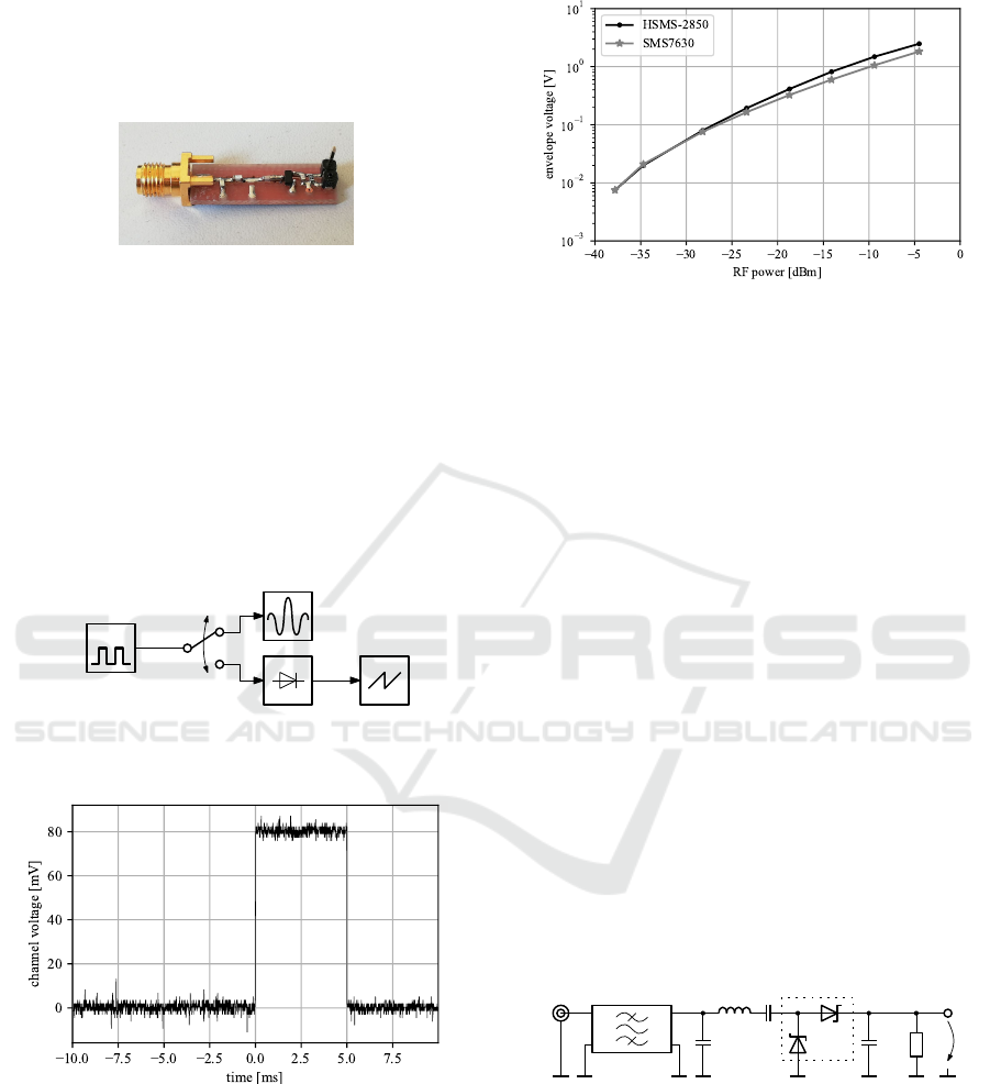
a printed circuit board (PCB) was made. Figure 4
shows one of these boards. The used circuit consists
of a matching circuit, the diode, and a low-pass filter
with resistive load at the end.
Figure 4: Picture of the PCB used for the diode selection
tests. From left to right: SMA connector, matching circuit,
diode, low-pass filter with resistive load.
In figure 5 the block diagram of the measurement
setup is seen. The signal generator produces a RF car-
rier pulse of a length of 5 ms. The power of the signal
generator can be adjusted and is measured by a spec-
trum analyzer. The test signal is fed into one of the
test boards. An oscilloscope measures the output sig-
nal. A typical output response can be seen in figure 6.
This picture was captured at a RF power of −30 dBm
with the diode HSMS-2852.
G
RF Signal Generator
Spectrum Analyser
Test Circuit
Oscilloscope
Figure 5: Block diagram of measurements for the diode
comparison.
Figure 6: Typical waveform of the envelope detector output
generated by a 5 ms carrier pulse. Captured by an oscil-
loscope, a test circuit with the HSMS2852 diode at a RF
power of −30 dBm.
To compare both diodes the amplitude of the re-
sulting envelope waveform was captured at multiple
voltage levels. The results are seen in figure 7. It is
worth mentioning that the signal at an output power
of −37.8 dBm is the last measurable by our setup.
For measuring at lower input levels, an additional
pre-amplifier is needed. The experiment showed that
Figure 7: Voltage sensitivity curve of the two selected
diodes.
the transmission properties of both diodes are nearly
identical. Especially at lower input powers, the volt-
age sensitivity curves match exactly. A typical volt-
age sensitivity of both diodes is γ = 80 mV/µW. This
test shows that the diode SMS7630-006LF is a good
replacement for the HSMS-2852. For the following
tests, in the envelope detector circuit, the SMS7630 is
used.
4.2 Radio Frequency Circuit
The schematic of the RF circuit can be seen in fig-
ure 8. An SMA connector realizes the RF input. It
allows the connection to both a signal generator or
an antenna. The SAW filter is a typical filter for the
868 MHz band. The components L
1
and C
1
match
the impedance of the envelope detector to 50 Ω. As
described previously, a Greinacher voltage doubler
boosts the performance of the envelope detector. The
output voltage is converted and filtered by the compo-
nents R
1
and C
3
. These components act as a low-pass
filter. Only the LF components of the signal are re-
maining.
IN
OUT
SMA
868 MHz
SAW Filter
Connector
C
1
L
1
Impedance
Matching
V
out
C
2
Greinacher
Voltage Doubler
C
3
R
1
Low-Pass
Filter
D
1
Figure 8: Schematic of the RF part of the proposed imple-
mentation of the carrier sensing circuit.
In comparison to the previous test circuits, a SAW
filter is added. To show the impact of the SAW filter
on the voltage sensitivity of the circuit, the previously
made tests were repeated with this circuit. The test
results can be seen in figure 9.
The output voltage with the SAW filter is signif-
An Efficient Low-power Wake-up Receiver Architecture for Power Saving for Transmitter and Receiver Communications
65
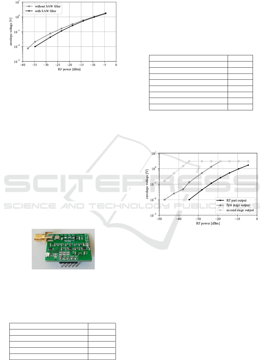
Figure 9: Voltage sensitivity curve with and without the
SAW filter.
icantly smaller. The additional transmission losses
introduced by the filter explain this behavior. This
trade-off has to be made to ensure proper filtering
of the RF signal against signals on other frequency
bands.
The average voltage sensitivity of the proposed RF
part can be calculated from the experimental results
and is about 28 mV/µW. It can be estimated that an
output voltage of around 280 µV is generated at a RF
input power of −50 dBm. This figure will be used to
define the parameters of the amplifier and comparator
circuit.
4.3 Test Circuit
In figure 10 a picture of the test PCB can be see. The
RF circuit in the upper part was specially matched for
the PCB. In the lower part, the LF circuit is imple-
mented. The two Op-Amps and the comparator are
populated.
Figure 10: Picture of the PCB used for the system test.
The table 2 shows the parameters of the used com-
parator. The threshold voltage was set to 100 mV
because of the maximum input offset voltage of the
comparator.
Table 2: Parameters of the comparator circuit.
Supply voltage 3.0 V
Comparator TLV3691
Typical current consumption 75 nA
Typical propagation delay 45 µs
Maximum input offset voltage ±15 mV
Threshold voltage 100 mV
The table 3 shows the parameters of the ampli-
fication circuit. A total amplification of factor 900
achieves a carrier sensing at input powers less than
−50 dBm. Two stages in series realize this amplifica-
tion. The resulting settling time was calculated with
equation 4. The biasing voltage was selected accord-
ing to the Op-Amp’s input offset voltage.
Table 3: Parameters of the amplifier circuit.
Total amplification factor 900
Number of amplifier stages 2
Amplification per stage 30
Operational amplifier TLV521
Typical current consumption 350 nA
Typical GBWP 6 kHz
Maximum input offset voltage ±3 mV
Settling time 2.4 ms
Biasing voltage 3 mV
To ensure that the circuit is working properly the
typical test procedure described early was repeated.
Both output signals of the amplification stages were
monitored. The results of this test can be seen in fig-
ure 11.
Figure 11: Voltage sensitivity curve of RF circuit and both
amplifier stages.
The amplification of the test signal was measured
to a minimum input power of −47 dBm. The ampli-
tude of the signal reached 165 mV. This output signal
together with the comparator output can be seen in
figure 12.
For greater input signals the output signal is
clamped to the supply voltage, but the comparator
output is still present. The calculation of the power
consumption can be seen in table 4. This total power
consumption of around 1.4 µA was also verified by a
bench multimeter.
4.4 Usage as a Wake-up Receiver
The proposed carrier sensing circuit can be used on
both sides of the transmission chain. The first usage
- on the transmitter side - is carrier detection. The
second usage - on the receiver side - is an ultra-low-
SENSORNETS 2021 - 10th International Conference on Sensor Networks
66
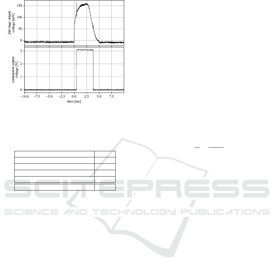
Figure 12: Typical waveform of the second amplifier stage
output and the comparator signal. Captured by an oscil-
loscope, the carrier sensing test circuit at a RF power of
−47 dBm.
Table 4: Calculated current consumption of the proposed
carried sensing circuit.
Component I [nA]
Biasing Circuit 300
Amplifier 700
Comparator 75
Comparator threshold generation 300
Total 1375
power wake-up receiver.
To test the usability of the circuit as a wake-up
receiver a radio transceiver module is used. A car-
rier pulse at the center frequency of 868.0 MHz at an
output power of 10 dBm is generated. Two λ/2 whip
antennas are used for the transmitter and the carrier
sensing test circuit. On the output of the test circuit,
a LED is added. With this setup, a maximum trans-
mission range of around 10 m can be observed. In-
terferences of other RF systems are present but less
frequent.
5 DISCUSSION AND
CONCLUSION
5.1 Further Work
The proposed carrier sensing circuit shows a simple
way to implement a wake-up receiver without any
specialized integrated circuits, like microcontrollers
or LF wake-up receiver chips. The RF part of the cir-
cuit is kept simple. Additional work in the LF ampli-
fication circuit has to be done. More tests have to be
made, to investigate whether the power consumption
can be reduced by using the inverting amplifier. The-
oretically, the biasing circuit can be replaced by an
ultra-low power voltage regulator. Additional power
savings for the comparator threshold generation are
possible too.
Currently, the circuit was only built for a carrier
frequency of 868 MHz. By swapping the SAW filter
and matching the RF circuit other frequency bands
can be used. Further tests will be made to test the
circuit’s performance in the 433 MHz and 2.4 GHz
range. The 2.4 GHz range is highly important due to
its capability to realize high data rate transmissions.
The transmission loss of the RF signal and the re-
sulting range is dependent on the wavelength. This
can be explained by the Friis transmission formula,
seen in equation 5 where P
r
and P
t
are the received and
transmitted power, A
r
and A
t
the effective aperture of
the corresponding antennas, d the distance, and λ the
wavelength.
P
r
P
t
=
A
r
·A
t
d
2
·λ
2
(5)
The effect of the lower transmission range has to be
observed and what applications are suitable when us-
ing the circuit at 2.4 GHz.
5.2 Usability as a Wake-up Receiver
As described in section 4.4 a carrier pulse of 5 ms
can be used as a wake-up signal and can be received
within a range of 10 m. Because no additional filter
techniques are applied (e. g. modulation frequency
detection or address matching) all RF packages with
matching power and duration are detected.
This is why this circuit is specialized for an envi-
ronment with low interferences from other RF com-
ponents. When there are only a few participants in
the wireless network address filtering is not needed.
The latency and current consumption of these wire-
less networks can be reduced significantly. We are
planning to use this circuit for a measurement system
located inside a shielded machine gearbox. In this use
case interferences are very low. The benefits of the
implementation lie in a significant decrease in power
consumption and latency time. When using this cir-
cuit in a different environment, it is clear, that further
filtering techniques are needed.
5.3 Usability as a Carrier Sense Circuit
The second usage is found in carrier detection and
collision avoidance techniques. When communicat-
ing in a wireless network package collision is quite
An Efficient Low-power Wake-up Receiver Architecture for Power Saving for Transmitter and Receiver Communications
67

frequent. These collisions result in an energy loss be-
cause the current package needs to be resent.
This energy loss E
loss
through one package col-
lision can be approximated by the equation 6. The
collision probability p
col
was estimated at 30 %, the
package duration t
P
at 5 ms, the transmission current
consumption I
T
at 25 mA and the supply voltage V
S
at
3.3 V.
E
loss
= p
col
·t
P
·I
T
·V
S
= 124 µJ (6)
To put this value of 124 µJ into relation, the time,
which the carrier sense circuit can stay active with this
energy, can be calculated by equation 7.
t
active
=
E
loss
V
S
·I
S
= 26.8 s (7)
Because the carrier sense circuit is only used a
fraction of a time to ensure no carrier is active on the
channel, the carrier sense circuit’s power loss is nearly
negligible.
Modern wireless transceiver modules often have a
carrier sensing circuit, clear channel assessment mod-
ule, or wake-on radio integrated. The improvement is
much better sensitivity and selectivity. But when tak-
ing a look at typical current consumptions of these
modes, they are in the order of 10 mA (Atmel, 2014).
Comparing this current consumption to the current
consumption of the proposed circuit it is very clear
that an improvement of factor 7000 can be achieved.
5.4 Conclusion
In this work, a power-saving approach with energy
detection and carrier sensing is presented. When us-
ing the circuit in a receiver it turns on only when
a carrier signal is detected at a carrier frequency of
868 MHz. This setup observes a maximum transmis-
sion range of around 10 m and total power consump-
tion of 4.2 µW. Further development of the circuit is
planned not only to be used at 868 MHz but also to
be designed for other frequency bands. Further tests
will be made to test the circuit’s performance in the
433 MHz and 2.4 GHz range. The 2.4 GHz range is
very important due to its capability to realize high
data rate transmissions.
REFERENCES
Agilent Technologies (2003). Agilent RF and Microwave
Test Accessories: Detector Overview.
Ammar, Y., Bdiri, S., and Derbel, F. (2015). An ultra-
low power wake up receiver with flip flops based ad-
dress decoder. In 2015 IEEE 12th International Multi-
Conference on Systems, Signals & Devices (SSD15),
pages 1–5. IEEE.
Atmel (2014). AT86RF233 - Low Power, 2.4GHz
Transceiver for ZigBee, RF4CE, IEEE 802.15.4,
6LoWPAN, and ISM Applications.
Bannoura, A. (2016). Algorithms and Applications for Low
Power Wireless Sensor Networks using Wake-up Re-
ceivers.
Bdiri, S., Brini, O., and Derbel, F. (2018a). Digital Back-
end Based on a Low-power Listening Protocol for
Wake-Up Receivers. In Sensors & Transducers, vol-
ume 224, pages 22–27.
Bdiri, S. and Derbel, F. (2014). A nanowatt Wake-Up Re-
ceiver for industrial production line. In 2014 IEEE
11th International Multi-Conference on Systems, Sig-
nals & Devices (SSD14), pages 1–6. IEEE.
Bdiri, S., Derbel, F., and Kanoun, O. (2018b). A Tuned-
RF Duty-Cycled Wake-Up Receiver with −90 dBm
Sensitivity. volume 18.
Bdiri, S., Derbel, F., and Kanoun, O. (2018c). A wake-up
receiver for online energy harvesting enabled wireless
sensor networks. In Kanoun, O., editor, Energy Har-
vesting for Wireless Sensor Networks, pages 305–320.
De Gruyter.
Del Prete, Massimo an Masotti, D., Costanzo, A., Magno,
M., and Benini, L. (2016). A dual-band wake-up ra-
dio for ultra-low power Wireless Sensor Networks. In
2016 IEEE Topical Conference on Wireless Sensors
and Sensor Networks, pages 81–84, Piscataway, NJ.
IEEE.
Horowitz, P. and Hill, W. (2015). The Art of Electronics.
Cambridge University Press, USA, 3rd edition.
Magno, M., Jelicic, V., Srbinovski, B., Bilas, V., Popovici,
E., and Benini, L. (2016). Design, Implementa-
tion, and Performance Evaluation of a Flexible Low-
Latency Nanowatt Wake-Up Radio Receiver. IEEE
Transactions on Industrial Informatics, 12(2):633–
644.
Meinke, H. and Gundlach, F.-W. (1986). Taschenbuch
der Hochfrequenztechnik. Springer Berlin Heidelberg,
Berlin, Heidelberg, vierte, v
¨
ollig neubearbeitete au-
flage edition.
Pletcher, N. (2008). Ultra-low power wake-up receivers for
wireless sensor networks: Dissertation. University of
California at Berkeley.
Polonelli, T., Le Huy, T., Lizzi, L., Ferrero, F., and Magnod,
M. (2016). A wake-up receiver with ad-hoc antenna
co-design for wearable applications. In SAS Sensors
Applications Symposium, pages 1–6, Piscataway, NJ.
IEEE.
Skyworks Solutions, Inc. (2008). Mixer and Detector
Diodes.
Spenza, D., Magno, M., Basagni, S., Benini, L., Paoli, M.,
and Petrioli, C. (2015). Beyond Duty Cycling: Wake-
up Radio with Selective Awakenings for Long-lived
Wireless Sensing Systems.
SENSORNETS 2021 - 10th International Conference on Sensor Networks
68
