
High Uniformity Design of UV LED Illuminators for Exposure
Equipment
Chun-Han Chou
1,
*
a
, Yu-Hsuan Lin
1b
, Hsin-Yi Tsai
1c
, Ray-Ching Hong
1
and Yi-Yung Chen
2d
1
National Applied Research Laboratories, Taiwan Instrument Research Institute, 20 R&D Rd. VI, Hsinchu Science Park,
Hsinchu City 30076, Taiwan
2
Graduate Institute of Color & Illumination Technology, National Taiwan University of Science and Technology,
No.43, Keelung Rd., Sec.4, Da’an Dist., Taipei City 10607, Taiwan
Keywords: Lithography, Irradiance Measurement, Uniformity, REMA Lens System, UV LEDs.
Abstract: We have presented the optical system design of control uniformity illumination system for stepper lithography.
The illumination system acted a key factor in the lithography, because the output light source quality affected
the exposure resolution and yield rate of products. The illumination system was composed by seven lens,
imaging field was 12.6mm, chief ray angle was less than 0.4 degrees, distortion was less than 0.47% and
numerical aperture was 0.1644. the irradiance flux of target area average was about 20 mW/cm
2
. The system’s
uniformity deviation was less than ± 3 percentages. Each UV-LED of illumination system was individually
controlled. It could make the imaging plane always have high uniformity to overcome the problem of light
source attenuation.
1 INTRODUCTION
Currently, the integration circuit was rapidly
developing to high density and high productivity by
the lithography, pattern transfer and process
technology. While early integration circuits features
were 25mm, currently manufactured features were
less than 20 nm. The integration circuits of feature
size, separation of structures and layer-to-layer
registration were decreased by approximately 30%
linearly per generation and doubling of the density of
transistors each generation (Moore, 1998). It has
become what we know as "Moore's Law."
The exposure process was the most important
technology in the integration circuit fabrication. It
could directly affect the size of integrated circuits,
wafer utilization and productivity. Lithography
equipment usually composed by the illumination
system, projection lens system and movement
platform and it was used for exposure process
(Rueggeberg and Caughman et al., 1994). The
illumination system used to modify the light source
a
https://orcid.org/0000-0003-2460-5875
b
https://orcid.org/0000-0002-1981-0359
c
https://orcid.org/0000-0001-8275-6132
d
https://orcid.org/0000-0002-0966-5784
meted the request of numerical aperture, illumination
field and uniformity etc. The illumination system
output light source illuminated on the reticle and the
reticle pattern transfer to the wafer by projection lens
system. The illumination system acted a key factor in
the lithography, because the output light source
quality affected the exposure resolution and yield rate
of products. In the industry, the common lithography
equipment was proximity mask aligner. It had the
advantages of large area exposure and simple device
structure etc. In the 2010 years, Reinhard Voelkel
team created an illumination system which had two
microlens-based Köhler integrators. The Light source
output was telecentric and high uniformity. The
system resolution was 10um (Voelkel and Vogler et
al., 2010). In the 2010 years, S. Partel team created a
new illumination system for SUSS mask aligner using
two consequent optical integrators and an
exchangeable illumination filter plate. The filter plate
could reduce the interference effected to increase the
system resolution. The system resolution is 2um
(Partel and Zoppel et al., 2010). However, the
proximity mask aligner system resolution closed to
68
Chou, C., Lin, Y., Tsai, H., Hong, R. and Chen, Y.
High Uniformity Design of UV LED Illuminators for Exposure Equipment.
DOI: 10.5220/0010222300680072
In Proceedings of the 9th International Conference on Photonics, Optics and Laser Technology (PHOTOPTICS 2021), pages 68-72
ISBN: 978-989-758-492-3
Copyright
c
2021 by SCITEPRESS – Science and Technology Publications, Lda. All rights reserved
the nanometer, this kind of lithography structure was
not valid for mass production and a single defect
already made a complete microchip unusable.
For this reason, many people turned to research
step lithography systems. It had the advantage of the
higher resolution, low cost of reticle and easy to mass
production. In the 1986 years, Victor Pol team
presented a stepper lithography which light source
was KrF excimer laser (248nm). The lighting system
had the numerical aperture of 0.38 and the imaging
field greater than 14.5 mm. The system resolution
was 0.8um (Pol and Bennewitz et al., 1986). In the
2008, Rosanne M. Guijt team presented a low cost UV-
LED lithography which used a pinhole and a small
plastic tube and focused using a microscope objective
onto a substrate for direct lithographic patterning of the
photoresist. The system resolution was higher than 20
μm (Guijt and Breadmore, 2008). In the 2016 years,
Hans-Christoph Eckstein teams presented a UV LED
lithography which could be demagnified five to one
hundred times and position accuracy was higher than
100 nm (Eckstein and Zeitner et al., 2016). In the
prior art, people created lithography illumination
system by mercury lamp, LED or laser. When used
for long periods of time, these light sources attenuated
to affect output uniformity and flux. It declined the
yield rate of product.
Therefore, in the studying, we presented a control
uniformity illumination system for stepper
lithography. Each UV-LED of illumination system
was individually controlled. It could make the
imaging plane always have high uniformity to
overcome the problem of light source attenuation.
The illumination system composed by UV-LED,
reflector, REMA lens system and light source
controller. The UV-LED emission light intensity
distribution was changed by the reflector and coupled
to the projection lens system. The REMA lens system
organized the input ray to be user defined light
intensity distribution and illumination field size. The
controller was used to control each UV-LED output
efficiency made the imaging plane always has high
uniformity.
2 THE OPTICAL DESIGN OF
ILLUMINATION SYSTEM
Lithography is the key equipment in the integrated
circuit process and its’ Illumination quality was the
most important factor. It directly affected the size of
integrated circuit line per. There are three important
factors in the lithography illumination system
(Weichelt and Bourgin et al., 2017):
• NA: The illumination system NA should
correspond with the project lens system,
otherwise the resolution of the projection
system will decrease.
• Uniformity: It effects the exposure depth of the
lines. The uniformity deviation usually lower
than 10%.
• Efficiency: It effects the system conversion
efficiency.
The illumination system was designed by the
sequential optical simulation software(Zemax) and
non-sequential optical simulation software(FRED).
The sequential optical simulation software was used
to optimize the imaging plane uniformity and third
aberration. The non-sequential optical simulation
software used to eliminate the effects of stray ray. The
list of design goals was as follows:
1. Imaging plane numerical aperture 0.165
2. Imaging plane uniformity deviation < ± 4 %
3. Imaging plane irradiance > 15 mW/cm
2
4. Imaging plane size > 20 x 8 mm
2
5. Chief ray angle < 0.5 degrees
6. Distortion < 0.5 %
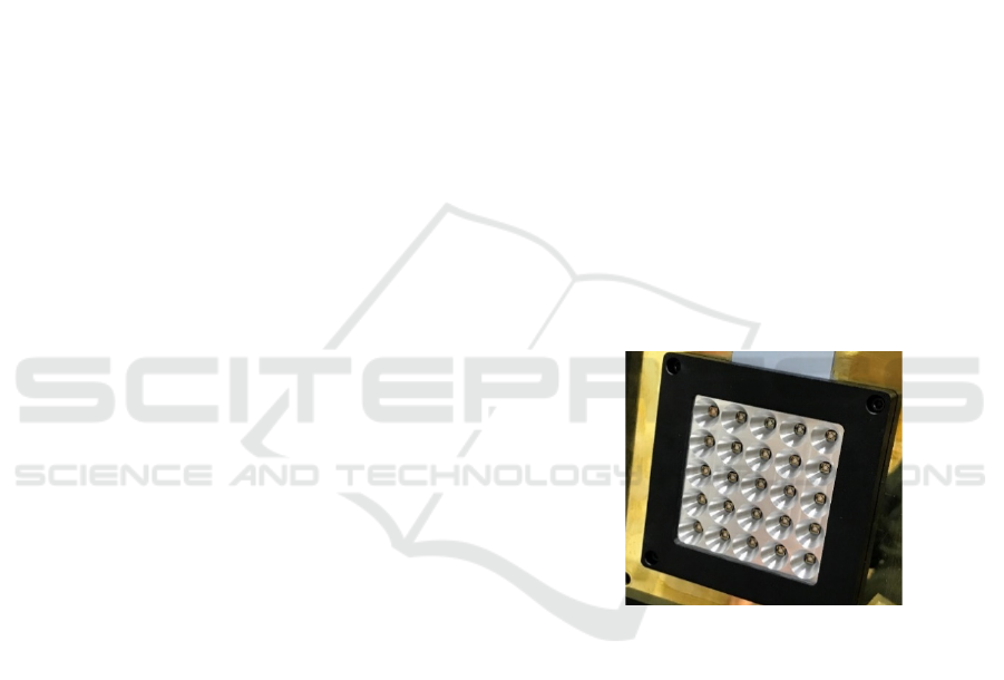
Figure 1: The UV-LED array arrangement.
The first step for design the illumination system
was to determine the light source parameters. When
the UV-LED(LTPL-C034UVH365) inputted 5V and
700mA, the UV-LED luminous flux was 720-
860mW. If the imaging plane irradiance should
higher than 15mW/ cm
2
, the UV-LED needed 5 x 5
chips array at least. In order to increase the utilization
rate of light source, the chips array coupled with a
reflector made the half of diverge angle of light
source less than 10 degrees, reference the Fig.1. The
REMA lens system was arranged behind the UV-
LED chips array. The REMA lens system was
designed by Köhler illumination (Köhler, 1893).
Köhler illumination proposed by August Köhler for
optical microscope illumination, allows to adjust the
size and the numerical aperture of the object
High Uniformity Design of UV LED Illuminators for Exposure Equipment
69
illumination in a microscope independent from each
other. Köhler illumination provides uniform
illumination of the object plane independent of shape,
extension and angular field of the light source.
2.1 Optical Design of REMA Lens
System
The lens system was designed by sequential and non-
sequential optical simulation software. The sequential
optical simulation software was used to design the
light path, optimize third aberrations and assemble
tolerance. The non-sequential optical simulation
software was used to analysis and eliminate stray ray
effects. Though these optical simulation, the
simulation results were more close to the fabrication
production.
2.1.1 Sequential Optical Simulation
In the optical simulation, the light source size was
30*30mm and half of divergence angle was 10
degrees. In order to reduce production price and error,
the lens radius and diameter should not exceed
500mm and 90mm, and the front and back radius of
each lens should differ by more than 10%. After the
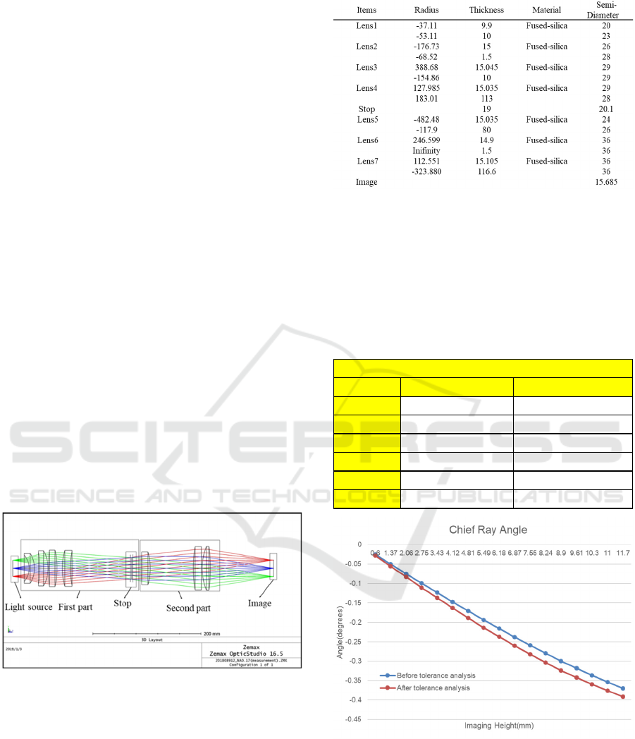
design, the lens system was composed by seven lens,
imaging field was 15.6mm, chief ray angle was less
than 0.4 degrees, distortion was less than 0.47% and
numerical aperture was 0.1644. The data referred to
the Fig.2. and Table. 1.
Figure 2: Optical light path diagram.
Table 1: The Lens data of the REMA lens system.
The simulation results of REMA lens system meted
the goal, the next step was doing tolerance analysis.
The tolerance analysis had two parts that were lens
manufacturing tolerance analysis and lens system
assemble tolerance analysis. The tolerance analysis
data referred to the Table. 2. After the tolerance
analysis, the simulation results still comply with the
target, referred the Fig. 3.
Table 2: Tolerance analysis data.
(a)
Itesms surface Tolerances Element Tolerances
Radius 0.00% non
Thickness 0.1mm non
DecenterX 0.3mm 0.1mm
DecenterY 0.3mm 0.1mm
Tilt X 0.3 degrees 0.1degrees
Tilt Y 0.3degress 0.1degress
Tolerance Parameters(wavelength: 365nm)
PHOTOPTICS 2021 - 9th International Conference on Photonics, Optics and Laser Technology
70
(b)
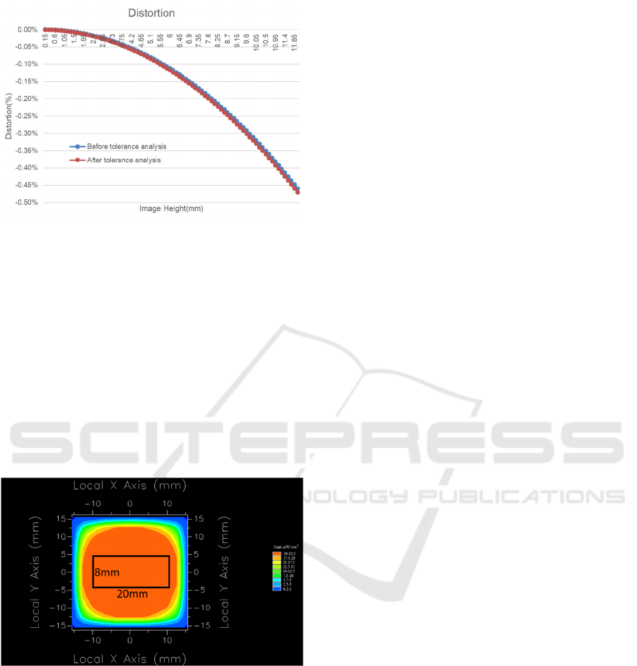
Figure 3: Third aberration data. (a).Chief ray angle
diagram. (b). Distortion diagram.
2.1.2 Non-sequential Optical Simulation
The targets of uniformity and irradiance was
simulated by non-sequential optical simulation
software. From the simulation results, the irradiance
flux of target area average was about 20 mW/cm
2
.
The system’s uniformity deviation was less than ± 3
percentages. It proves that the stray ray effect was
very low, the irradiance distribution referred Fig. 4.
Figure 4: The REMA lens output irradiance map.
3 DISCUSSION
In the studying, we presented a control uniformity
illumination system for stepper lithography. The
system had the 25 UV-LED. Each UV-LED could
individually control the output flux and the light
source switching frequency was less than 20 ms to
avoid flicker effect. The REMA lens system was
design by sequential and non-sequential optical
simulation software. After the tolerance analysis, the
simulation results still meted the targets.
4 CONCLUSION
We have presented the optical system design of
control uniformity illumination system for stepper
lithography. The lens system was composed by seven
lens, imaging field was 15.6mm, chief ray angle was
less than 0.4 degrees, distortion was less than 0.47%
and numerical aperture was 0.1644. The irradiance
flux of target area average was about 20 mW/cm2.
The system’s uniformity deviation was less than ± 3
percentages. In the future, we could add an intelligent
uniformity control algorithm and auto irradiance
measurement system. The irradiance measurement
system used to capture each point irradiance on the
imaging plane, and the data transferred to controller.
The controller controlled UV-LED flux by the
algorithm that make the imaging plane always have
high uniformity.
ACKNOWLEDGEMENTS
The authors would like to express their appreciation
for financial aid from the Ministry of Science and
Technology, R.O.C under grant numbers MOST 109-
2221-E-492-004. The authors would also like to
express their gratitude to the Taiwan Instrument
Research Institute of National Applied Research
Laboratories for the support.
REFERENCES
Moore, G. E. (1998). Cramming more components onto
integrated circuits. Proceedings of the IEEE, 86(1), 82-
85.
Rueggeberg, F. A., Caughman, W. F., & Curtis, J. W.
(1994). Effect of light intensity and exposure duration
on cure of resin composite. Operative dentistry, 19(1),
26-32.
Voelkel, R., Vogler, U., Bich, A., Pernet, P., Weible, K. J.,
Hornung, M., ... & Zeitner, U. D. (2010). Advanced
mask aligner lithography: new illumination system.
Optics express, 18(20), 20968-20978.
Partel, S., Zoppel, S., Hudek, P., Bich, A., Vogler, U.,
Hornung, M., & Voelkel, R. (2010). Contact and
proximity lithography using 193 nm excimer laser in
mask aligner. Microelectronic Engineering, 87(5-8),
936-939.
Pol, V., Bennewitz, J. H., Escher, G. C., Feldman, M.,
Firtion, V. A., Jewell, T. E., ... & Clemens, J. T. (1986,
August). Excimer laser-based lithography: a deep
High Uniformity Design of UV LED Illuminators for Exposure Equipment
71

ultraviolet wafer stepper. In Optical Microlithography
V (Vol. 633, pp. 6-16). International Society for Optics
and Photonics.
Guijt, R. M., & Breadmore, M. C. (2008). Maskless
photolithography using UV LEDs. Lab on a Chip, 8(8),
1402-1404.
Eckstein, H. C., Zeitner, U. D., Leitel, R., Stumpf, M.,
Schleicher, P., Bräuer, A., & Tünnermann, A. (2016,
March). High dynamic grayscale lithography with an
LED-based micro-image stepper. In Optical
Microlithography XXIX (Vol. 9780, p. 97800T).
International Society for Optics and Photonics.
Weichelt, T., Bourgin, Y., & Zeitner, U. D. (2017). Mask
aligner lithography using laser illumination for versatile
pattern generation. Optics express, 25(18), 20983-
20992.
Köhler, A. (1893). Zeitschrift für wissenschaftliche.
Mikroskopie X, 433-440.
PHOTOPTICS 2021 - 9th International Conference on Photonics, Optics and Laser Technology
72
