
Current Loop Stability Analysis of a VIENNA-type Three-phase
Rectifier for an Imaging System Power Supply Application
Matthieu Darnet
1 a
, Emmanuel Godoy
1 b
, Daniel Sadarnac
2
and Stephane Gautrais
3
1
Laboratoire des Signaux et Syst
`
emes (L2S, UMR 8506), CentraleSup
´
elec, CNRS,Universit
´
e Paris-Sud,
Universit
´
e Paris-Saclay, 3, Rue Joliot-Curie, 91192, Gif-sur-Yvette, France
2
Group of Electrical Enginering Paris (GEEPS, UMR 8507), CentraleSup
´
elec, Univ. Paris-Sud, Universit
´
e Paris-Saclay,
Sorbonne Universit
´
es, UPMC Univ Paris 06, 3 & 11 rue Joliot-Curie, 91192 Gif-sur-Yvette, France
3
X-Ray Generation, Imaging Sub-System, GE Healthcare, 283, Rue de la Mini
`
ere, 78530, Buc, France
Keywords:
VIENNA-type Rectifier, Stability Margins, Inner Current Loop Control, Input Filter, Resonance, System
Modelling.
Abstract:
High power supply for imaging systems needs to meet increasing demand in speed, power and voltage control.
A Vienna-type three-phase rectifier prototype has been developed by GE Healthcare to handle it. This power
supply has a significant stability issue because its load has a pulsed profile, and the ranges of power demand,
input voltage, and grid impedance are wide. First, a model of the rectifier and its control has been made.
Second, a current loop stability analysis has been investigated. Stability margins have been drawn for all the
range of output power, input voltage and grid inductance for the current loop. Stability has been shown for all
the operating points. However, a poorly damped input filter brings potential oscillations and reduces stability
margins. Delay margins are also particularly low. Finally, a validation of the rectifier model has been made
with measurements on the prototype.
1 INTRODUCTION
High-power imaging systems (MRI, X-ray scan-
ner,etc...) are powered from the Hospital power grid
through a multi-converters which has the following
functions :
• An AC/DC conversion to provide a DC voltage
for main load (X-Ray Generators) ;
• An isolation from grid;
• A DC/AC conversion to provide an AC three-
phase voltage for auxiliary loads;
The AC/DC Converter has to handle large constraints:
• Step power from a few kilowatts to a hundreds
kilowatts from main load;
• Transparent mode operation despite a wide
range of nominal input voltage and input grid
impedance.
In order to improve image quality, these systems
need accurate dc voltage regulation to increase the
power and speed for capturing images.
a
https://orcid.org/0000-0001-9727-2755
b
https://orcid.org/0000-0001-9114-8729
There are also additional industrial constraints on
cost and volume which must be taken into account
when designing a new power supply.
Until now, the AC/DC converter is a passive three-
phase rectifier. And the low-frequency three-phase
transformer which provides the isolation has a big
volume. Consequently the output DC voltage is un-
regulated, the power supply has a low efficiency and
a large volume, although its cost is low. Thus it limits
the available peak power and the slope of pulsed load.
Active three-phase unidirectional rectifier ad-
dresses output voltage regulation, high efficiency, low
volume. It enables also the use of a smaller high fre-
quency transformer. Among the active rectifier, the
Vienna topology has a regulated output, good relia-
bility, good power density, a low total harmonic dis-
tortion and is well documented (Leibl, 2017) (Kolar
and Friedli, 2011). A prototype of an modified Vi-
enna (cf. Fig. 3) has been successfully built by GE
Healthcare and validated for several operating points.
In order to validate this topology and its control
strategy, this paper investigates the stability margins
on a wider range of operating points. The control
model of Vienna (cf. Fig. 5) is made of three con-
trol loops on input currents, total output voltage and
output midpoint voltage. The main stability issues ap-
Darnet, M., Godoy, E., Sadarnac, D. and Gautrais, S.
Current Loop Stability Analysis of a VIENNA-type Three-phase Rectifier for an Imaging System Power Supply Application.
DOI: 10.5220/0009828605850593
In Proceedings of the 17th International Conference on Informatics in Control, Automation and Robotics (ICINCO 2020), pages 585-593
ISBN: 978-989-758-442-8
Copyright
c
2020 by SCITEPRESS – Science and Technology Publications, Lda. All rights reserved
585
pears in the input currents control loop because it is
the fastest loop. Consequently only the current loop
will be studied. A single variable approach has been
chosen to clearly highlight the main issues regarding
resonances and stability margins.
The paper is organized as followed. Section 2 de-
scribes a model of the modified Vienna Rectifier and
its control strategy. Section 3 draws the stability mar-
gins of the current loop over one phase from a lin-
earised averaged model. A sweep of output power,
input nominal voltage and grid inductance shows the
weakest operating points. Section 4 shows a valida-
tion of the model by comparison with measurements
of the total output voltage and of one input current un-
der a power load step. Section 5 concludes the main
finding of this paper and discusses future work.
2 RECTIFIER MODELLING AND
CONTROL
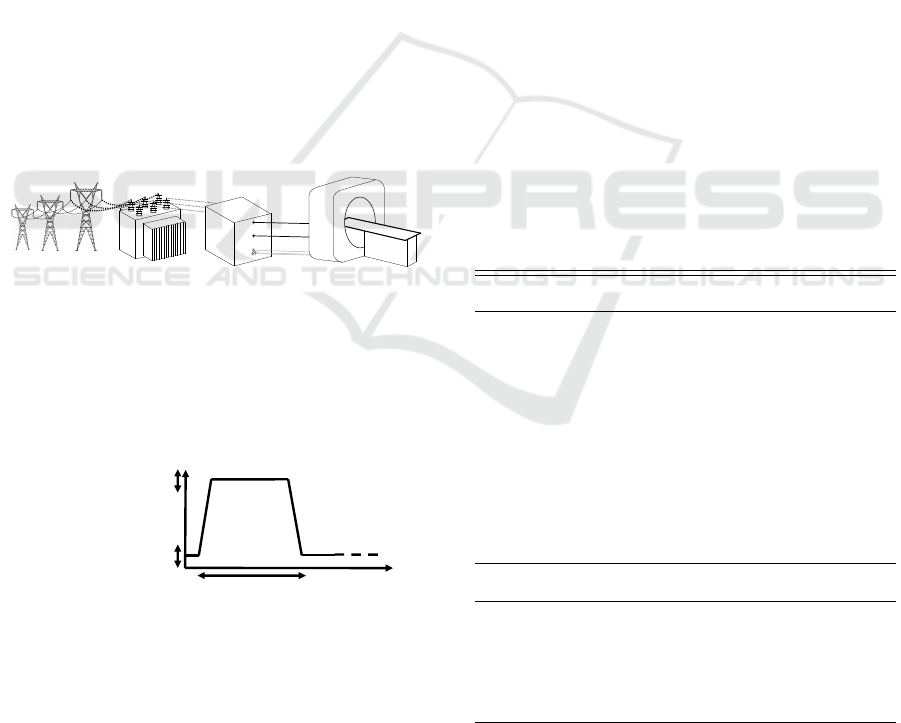
Fig. 1 shows how the power is supplied to the imaging
system. A transformer makes a connection between
power grid and hospital’s grid. It limits the available
power to 150kVA.
Electrical Grid
Hospital
Transformer
150kVA
Power Supply
Medical
Imaging System
DC Network
AC Network
Figure 1: Power transmission chain between power grid and
medical imaging systems.
Load profile is shown in Fig. 2. Power sup-
ply must face with low average power and high peak
power.
Pulse Duration :
20ms to 1min
Pout Pulse :
40 to 140kW
Pout RMS :
10 to 30kW
Figure 2: Load profile seen by power supply of a x-ray scan-
ner.
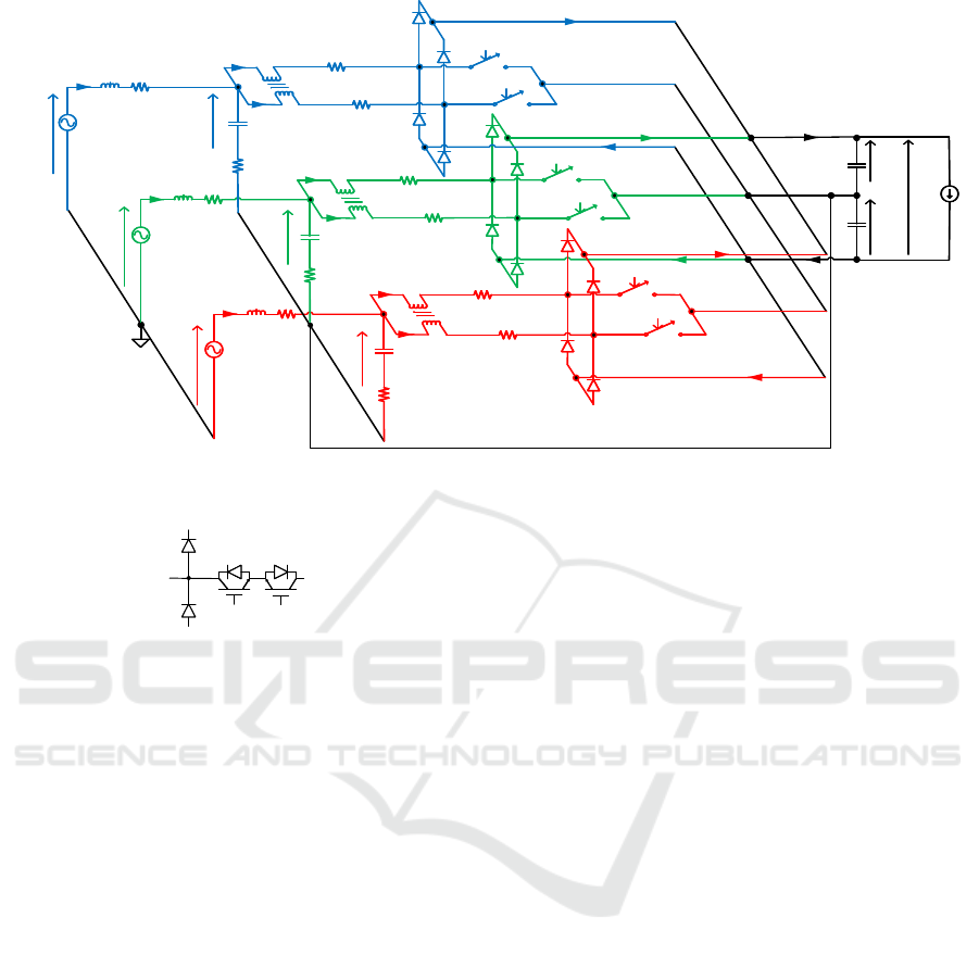
2.1 Rectifier Topology
Rectifier topology (cf. Fig.3) is composed by two in-
terleaved Vienna (Kolar and Friedli, 2011) and cou-
pled boost inductances for each phase. This is why it
has been named Coupled-Inductances Interleaved Vi-
enna Rectifier (C2IV Rectifier).
A two parallel converters topology has been cho-
sen to divide current constraints on semiconductors
by two.
The input phase voltages V
a
,V
b
and V
c
are ideal
three-phase voltage source. The grid line between
phase voltages and C2IV is modelled by an induc-
tance L
g
in series with a resistance R
g
.
The input filter is composed by three capacitors
C
x
in star connection with their parasitic resistors R
x
in series. The artificial neutral point of this filter is
connected to the ouptut midpoint voltage M for com-
mon mode filtering.
Boost Inductances L of phase 1 and 2 are cou-
pled. (COSTAN, 2007) shows the advantages of in-
ductances coupling. Combined with an interleaved
command of the two phase of the converters, current
ripples in grid and in inductances see their amplitude
divided by two and their frequency multiplied by two.
Consequently, inductance size can be reduced for the
same constraints in current ripple.
The chosen bidirectional switch is a T-type bridge-
leg structure (cf. Fig.4) with two IGBT and two an-
tiparallel diodes. Its main advantage is low cost be-
cause of its usage for three-phase inverters.
Table 1 shows the value of hardware parameters
of the C2IV prototype.
Table 1: Simulation Parameters.
Invariant Parameters Units Value
Output DC voltage V
dc
V
800
Output capacitors C
µF 4240
Boost inductance L
µH 800
Boost mutual M
µH
760
Intern resistance R
l
mΩ
100
Input capacitors C
x
µF 10
Parasitic resistance Rx
mΩ
3
Grid frequency f
grid
Hz
50
Switching frequency f
sw
kHz
23
Variable Parameters Units Min
Max
Ouptut power P
out
kW
10 140
Input AC voltage V
in
V
llrms
342
528
Grid inductance L
g
µH 10 300
Grid resistance R
g
mΩ
10 120
ICINCO 2020 - 17th International Conference on Informatics in Control, Automation and Robotics
586
M
Io
++
C2
Lg
Rg
Cx
C
C
L
Vc
Ic2
Vc1
Vc2
Dc2
L
Ic1
C1
Dc1
Ic
Vxc
++
N
Lg
Rg
Cx
Vb
Ib1
Ib
Vxb
++
Lg Rg
Cx
Va
Ia1
Ia
Vxa
Ib2
Ia2
L
L
L
L
B2
A2
Da2
Da1
Db2
Db1
A1
Iap
Ian
Ibp
Icp
Ibn
Icn
B1
Ip
In
M
M
M
M
P
P
P
A
B
C
Rl
Rl
Rl
Rl
Rl
Rl
Vdc
Rx
Rx
Rx
Figure 3: Schematic of the Coupled-Inductances Interleaved-Vienna Rectifier (C2IV) in a pseudo-3D view.
M
p
n
A
Figure 4: T-Type bridge-leg structure.
2.2 Rectifier Modelling
Assumptions made to obtain state space equations are
identical to what has already been done for Vienna
rectifier in (Lai et al., 2009) and will not be detailed.
Every identical variables (currents, voltages,
switch commands) are put together in vectors to sim-
plify the writing of differential equations.
For each inductance and each capacitor corre-
sponds a state variable as seen in Fig. 3. There are
14 state variables.
Input currents in boost inductances L are shown in
eq.1 :
I
abc12
= (
I
a1
I
b1
I
c1
I
a2
I
b2
I
c2
) (1)
Output voltages across the output capacitances C
are shown in eq.2 :
V
c12
= (
V
c1
V
c2
) (2)
Phase currents in grid inductances L
g
are shown in
eq.3 :
I
abc
= (
I
a
I
b
I
c
) (3)
Input filter voltages across capacitances C
x
are
shown in eq.4:
V
xabc
= (
V
xa
V
xb
V
xc
) (4)
There are 6 control variables shown in eq.5, be-
cause each bidirectional switch is controlled by only
one signal :
D
abc12
= (
D
a1
D
b1
D
c1
D
a2
D
b2
D
c2
) (5)
In real-time equations, D
abc12
stands for the switch-
ing states which take the value 0 or 1. In average
equations,D
abc12
stands for the duty-cycles .
Perturbation variables are the three phase voltages
(cf. eq.6) and the output current (cf. eq.7) :
V
abc
= (
V
a
V
b
V
c
) (6)
I
out
= (
I
o
I
o
) (7)
Matrices of coupling inductances (cf. eq.8), of
duty-cycles (cf. eq.9) and of input currents sign (cf.
eq.10) are used to further simplify writings of differ-
ential equations.
[
L M
] =
L 0 0 M 0 0
0 L 0 0 M 0
0 0 L 0 0 M
M 0 0 L 0 0
0 M 0 0 L 0
0 0 M 0 0 L
(8)
(1 − D
abc12
)[i,i] = 1 − Dk
i
(1 − D
abc12
)[i, j] = 0 if i 6= j
with k
i
∈
{
a1,b1,c1,a2, b2,c2
}
(9)
sign(I
abc12
)[i,1] = 1 i f Ik
i
> 0 else 0
sign(I
abc12
)[i,2] = −1 i f Ik
i
> 0 else 0
(10)
The equations of C2IV are finally obtained in
eq.11
Current Loop Stability Analysis of a VIENNA-type Three-phase Rectifier for an Imaging System Power Supply Application
587
dI
abc12
dt
= [
L M
]
−1
·
−R
L
· I
abc12
+
h
I
3
I
3
i
·V
xabc
−(1 − D
abc12
) · sign(I
abc12
) ·V
c12
dV
c12
dt
=
1
C
·
sign(I
abc12
)
T
· (1 − D
abc12
) · I
abc12
− I
out
dI
abc
dt
=
1
Lg
·
V
abc
− Rg · I
abc
− (V
xabc
−
1
3
·
∑
V
xabc
)
dV
xabc
dt
=
1
Cx
· (I
abc
− [
I
3
I
3
] · I
abc12
)
(11)
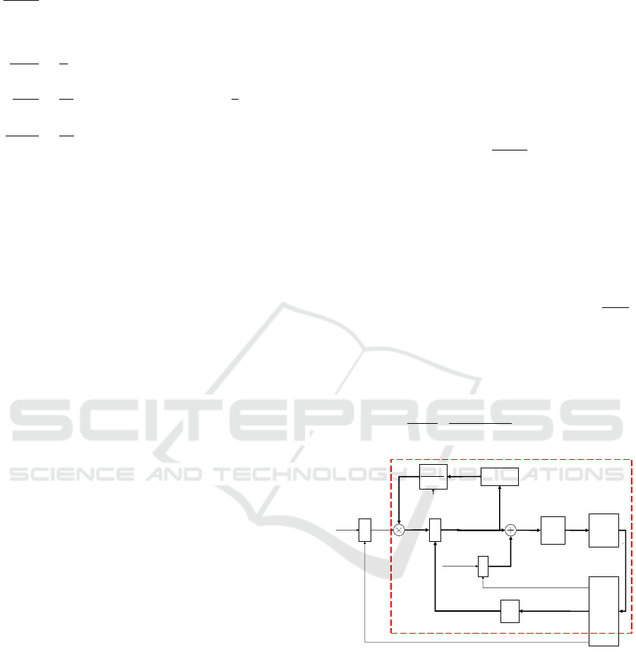
2.3 Rectifier Control
C2IV Rectifier control has a classic cascaded three
loops topology, as shown in Fig.5:
1. An inner loop on input currents I
abc12
is used to
control the Power Factor (PF) and Total Harmonic
Distortion of input currents (THD);
2. An outer loop on total output voltage V
dc
is used
to regulate V
dc
for a wide range of output power;
3. A third loop on the output midpoint voltage V
mid
is used to balance the two output voltages.
As one can often find in the literature, the outer
loop controller is a PI with the peak input current as
output. The third loop controller is a Proportional
controller which adds an offset on duty-cycles. These
loop are relatively slow.
The inner loop can be made in three different co-
ordinate systems :
1. In dq-frame (I
d
,I
q
) as in (Liu et al., 2017b) (Tang
et al., 2018), (Lai et al., 2009), (Ji et al., 2019) and
(Liu et al., 2017a) to take advantage of a constant
reference;
2. In αβ-frame (I
α
,I
β
) as in (Liu et al., 2018) to re-
duce control variables without using a complex
PLL like in dq-frame;
3. In abc-frame (I
a
,I
b
,I
c
) as in (Kolar and Friedli,
2011) and (Leibl, 2017) for simplicity.
Usually, a PI controller is used in dq-frame. A PI
controller in abc-frame has been chosen for this appli-
cation to simplify controller tunning. Moreover, abc-
frame could be more robust to a phase loss because
each phase is controlled independently.
Double carrier-based PWM is usually chosen (Liu
et al., 2017b), (Tang et al., 2018), (Ji et al., 2019) and
(Liu et al., 2017a). However a single carrier-based
PWM has been chosen for simplicity. It compares
duty-cycles from the output of inner loop with a single
carrier. This choice is made possible by the use of the
absolute value of currents as shown in Fig.5.
FPGA’s capability allows a PWM sampling at 50
MHz. It suppresses the usual PWM sampling delay.
Nevertheless the command, once changed by PWM
algorithm, must be blocked until the end of half of the
switching period to avoid command flickering.
The absolute currents reference in the inner loop
is given by eq.12 :
I
abc
re f
= I
peak
·
|
I
sinus
|
(12)
The absolute sinusoidal shape is given by eq.13 :
|
I
sinus
|
=
|
V
xabc
|
V
xpeak
(13)
As the measurements of voltage V
xabc
can be noisy,
an observer has been preferred. The eq.14 shows the
relation between input and output voltages and duty-
cycle for Boost-converter over one phase.
|
V
xabc
|
= (1 − D
abc12
)[k, k] ·V
c12
(14)
The output voltages V
c12
has been simplified by half
of the reference value of the total output voltage
V
dc
re f
2
.
The peak input voltage V
xpeak
has been simplified by
considering the maximum of the input voltages fil-
tered measurements, which is about 95% of peak in-
put voltage in three-phase. Thus the sinusoidal shape
is built like shown in eq.15.
|
I
sinus
|
=
V
dc
re f
2
·
1
max(V
xabc
)
· (1 − D
abc12
) (15)
Ipeak
Vienna
+
delays
PI
Vmid*
Dabc12
I
Vxabc
𝟏
𝑽𝒙
𝒑𝒆𝒂𝒌
Isinus
P
Iabc
ref
PI
Dmid
PWM
Sabc12
Observer
Abs
ADC
+
Filter
|Vxabc*|
Vdc
ref
Dabc12
Measures
Vmid=Vc1-Vc2
Vdc=Vc1+Vc2
Iabc12
Figure 5: Control block diagram of C2IV Rectifier.
3 CURRENT LOOP STABILITY
ANALYSIS
Linearising model of eq.11 around an operating point,
the linearised state space of C2IV Rectifier is obtained
in eq.16 :
˙
X = AX + BU
Y = CX + DU
(16)
ICINCO 2020 - 17th International Conference on Informatics in Control, Automation and Robotics
588
with the definitions of vectors in eq.17 :
State Vector X = (
I
abc12
V
c12
I
abc
V
xabc
)
Command Vector U = (
D
abc12
D
mid
)
Output Vector Y = (
|
I
abc12
|
V
mid
)
(17)
Once this linearized state space obtained, one can
draw the Bode Diagram between duty-cycles and in-
put currents, study resonances and stability margins.
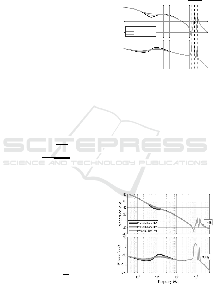
3.1 Input Filter Resonance Issue
Fig.6 shows that the current loop bandwidth
does not depend on phase voltage. Indeed,
the three curves corresponding to input voltages
(311V, −68V, −243V ) are superimposed for fre-
quency above 1kHz.
There are 3 resonances related to hardware in-
put parameters L
g
, C
x
, and leakage inductance L
f
(cf.
eq.18) of coupled boost inductances. One zero z
1
(cf.
eq.19) and two poles w
1
(cf. eq.20) and w
2
(cf. eq.21).
L
f
=
L − M
2
(18)
z
1
'
1
2π ·
p
C
x
· (L
g
+ L
f
)
(19)
w
1
'
1
2π ·
p
C
x
· L
f
(20)
w
2
'
1
2π ·
q
C
x
·
L
g
·L
f
L
g
+L
(21)
Resonances at w
1
(20) and w
2
(21) are poorly
damped. They are located above 10kHz, near the
switching frequency. It implies that the control model
cannot efficiently damp these resonances.
Furthermore, resonances move the location of sta-
bility margins to higher frequency, nearer to instabil-
ity.
A passive damping must be added to avoid poten-
tial oscillations and increase stability margins.
Switching frequency (cf. f
sw
in Table 1) limits
already the current loop bandwidth at 11kHz. The
presence of z
1
limits further the bandwidth at 2kHz
for high grid inductance.
Control parameters of Table 2 have been chosen
for this application.
The bode diagram of open current loop has been
drawn in Fig.7 combining transfer function of Fig.6
and transfer function of PI controller (cf. eq.22).
H
PI
(s) = K
p
1 +
1
T
i
s
(22)
A gain margin of 14dB and a phase margin of
36deg are acceptable margins.
10
20
30
40
50
60
70
Magnitude (dB)
Phase Ia1 and Da1
Phase Ib1 and Db1
Phase Ic1 and Dc1
10
1
10
2
10
3
10
4
-270
-180
-90
0
90
Phase (deg)
Frequency (Hz)
z1 w1 w2
Figure 6: Bode diagram between the three first duty-cycles
D
a1
, D
b1
, D
c1
and their corresponding input currents I
a1
,
I
b1
,I
c1
.
Table 2: Control Parameters.
Control Parameters Value
Current Loop PI Gains
Proportional Gain K
pI
5 × 10
−3
Constant Time Integral Gain T
iI
(s)
4 × 10
−5
Total Voltage Loop PI Gains
Proportional Gain K
pV
2.5
Constant Time Integral Gain T
iV
(s)
1.3 × 10
−3
Midpoint Voltage Loop P Gain
Proportional Gain K
pM
2 × 10
−3
Fig.7 also shows that phase margin is calculated
after high frequency resonances instead of around
2kHz where gain crosses first time at 0dB. The res-
onances are clearly not enough damped. As w
1
and
w
2
depend mainly on capacitors C
x
and leakage in-
Figure 7: Bode diagram of open loop current control.
Current Loop Stability Analysis of a VIENNA-type Three-phase Rectifier for an Imaging System Power Supply Application
589
ductance L f , a parallel damping circuit can be added
to one of these components.
A RC circuit in parallel with capacitors could be
the best good option. Indeed, the resistance R damps
the resonance. The capacitor C helps to decrease the
damping circuit losses by filtering low frequency har-
monics coming from the grid.
Fig.8 shows the effect of a resistor R
x
of 250mΩ in
series with each capacitor C
x
(cf. Fig.3). Resonances
are clearly damped. Phase margin is calculated here
around 2kHz.
Figure 8: Bode diagram of open loop current control with
input filter damping.
Nevertheless, damping three-phase input filter re-
quires a study in itself and there is an extensive liter-
ature on this subject.
For the rest, only a damping resistor of 3mΩ has
been added to take into account the parasitic resistors
of the real capacitors implemented on the prototype.
3.2 Stability Analysis
The variable parameters of Table 1 modify stability
margins. To understand where are the less stable op-
erating points, these margins have to be calculated for
all the domain.
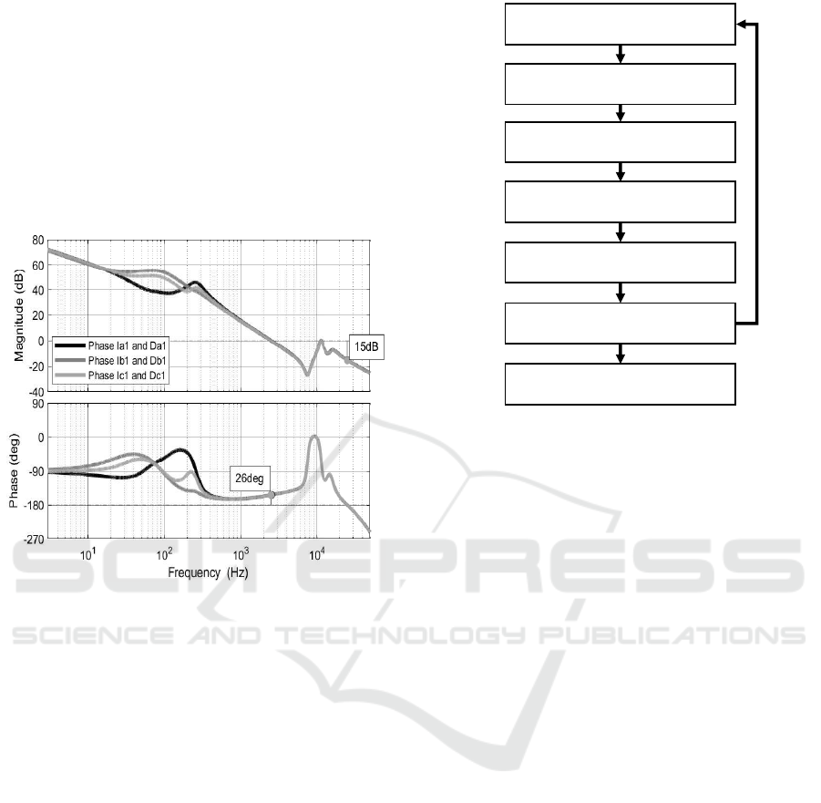
The process of Fig.9 have been used to get the sta-
bility margins for all the operating points. A simu-
lation model has been used to find a stable operat-
ing point for each choice of L
g
, P
out
and V
in
. Then,
the model has been linearised around these operating
points. Transfer function between duty-cycle and in-
put current have been obtained. Finally the margins
of open loop transfer function are calculated and com-
piled.
Fig.10, 11 and 12 show that the worst operating
Choose (Lg, Pout, Vin)
Simulate Average Model
(without PWM switching)
Extract Stable Operating Points
(𝐚𝐭 𝜽
𝒈𝒓𝒊𝒅
= 𝟏𝟎𝟖 𝒅𝒆𝒈)
Calculate Average State-Space Model
around found Operating Points
Calculate Open Current Loop Transfer
Function
Calculate Stability Margins
Evaluate the worst operating points of the
domain
Figure 9: Process to obtain Stability Margins from the
model and control of C2IV.
point considering stability margin is with low grid
inductance, high nominal input voltage and low out-
put power. The margins for the point (L
g
,V
in
,P
out
) =
(10µH,520Vrms, 10kW) are :
(Gain,Phase,Delay) = (8dB,25deg,3.5µs)
The minimum values of gain and phase margins
are acceptable.
However delay margins are particularly low. In-
deed, a synchronized PWM would have a zero order
hold (zoh) at twice the switching frequency (T
zoh
=
22µs) for interleaved rectifier. This would add a de-
lay at twice the period of the zoh (delay
zoh
= 11µs),
which is greater than the minimum delay on the do-
main.
Fig.10 shows that stability margins hardly depend
on grid inductance L
g
. Indeed, leakage inductance L
f
is very small compared to L
g
almost everywhere in the
domain. In this case, resonances w
1
(cf. eq.20) and w
2
(cf. eq.21) are approximately equal and independent
from L
g
.
Fig.11 shows that margins doesn’t depend much
on V
in
, particularly for a low inductance L
g
. For ex-
ample, the gain margin range for a sweep of V
in
varies
from less than 1dB to 5dB.
Fig.12shows that margins depends more on P
out
.
For example, the gain margin range for a sweep of
P
out
varies from 7dB to 10dB.
The curves of phase and delay margins of Fig.12
show a discontinuity between 40kW and 50kW for
(L
g
,V
in
) = (10µH,340V). It is explained by the fact
that margins are calculated for a frequency above w
2
ICINCO 2020 - 17th International Conference on Informatics in Control, Automation and Robotics
590
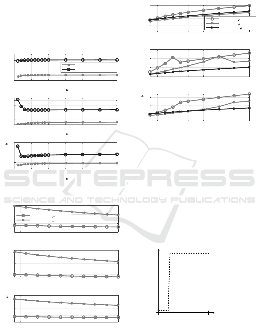
(cf. Fig.7) at low power. However depending on op-
erating points, the minimum margin can be calculated
for a frequency below w
2
.
Hence C2IV control should stay stable at every
operating point. However a better delay margin would
be preferable. This can be achieved by the damping
of input filter resonances.
0 50 100 150 200 250 300
Lg ( H)
5
10
15
20
25
Gain Margin (dB)
Gain Margin
(Pout,Vin)=(10kW,520V)
(Pout,Vin)=(140kW,340V)
0 50 100 150 200 250 300
Lg ( H)
20
30
40
50
60
70
Phase Margin (deg)
Phase Margin
0 50 100 150 200 250 300
Lg ( H)
0
5
10
15
20
Delay Margin ( s)
Delay Margin
Figure 10: Upper and lower bound of current loop stability
margins for a sweep of L
g
.
350 400 450 500
Vin (Vrms)
5
10
15
20
Gain Margin (dB)
Gain Margin
(Lg,Pout)=(10 H,10kW)
(Lg,Pout)=(10 H,140kW)
350 400 450 500
Vin (Vrms)
30
40
50
60
70
Phase Margin (deg)
Phase Margin
350 400 450 500
Vin (Vrms)
0
5
10
15
20
Delay Margin ( s)
Delay Margin
Figure 11: Upper and lower bound of current loop stability
margins for a sweep of V
in
.
20 40 60 80 100 120 140
Pout (kW)
0
5
10
15
20
Gain Margin (dB)
Gain Margin
(Lg,Vin)=(10 H,340V)
(Lg,Vin)=(10 H,520V)
(Lg,Vin)=(300 H,520V)
20 40 60 80 100 120 140
Pout (kW)
30
40
50
60
70
Phase Margin (deg)
Phase Margin
20 40 60 80 100 120 140
Pout (kW)
0
5
10
15
Delay Margin ( s)
Delay Margin
Figure 12: Upper and lower bound of current loop stability
margins for a sweep of P
out
.
4 MODEL VALIDATION
A comparison between measurements over a proto-
type and a Simulink-based Simulation has been made
to validate model of eq.11.
The parameters are taken from Table 1. Values of
the variable parameters for the comparison case are
shown in Fig.13. A resistive load has been connected
at the output of C2IV to make a power step from 1kW
to 60kW. It allows a comparison of the system dy-
namic of the control of output voltage V
dc
in Fig.14
and input currents I
a1
in Fig.15.
Pout (kW)
Time (ms)
60
0
1
5,1
26,2
Vin = 400 Vll
rms
Lg = 20µH
Rg = 100mΩ
Figure 13: Load step specification.
The absolute error between measurements and
simulation data have been drawn to have a closer look
at the differences between them. To remove harmon-
ics due to the switching frequency, a filtering have
Current Loop Stability Analysis of a VIENNA-type Three-phase Rectifier for an Imaging System Power Supply Application
591
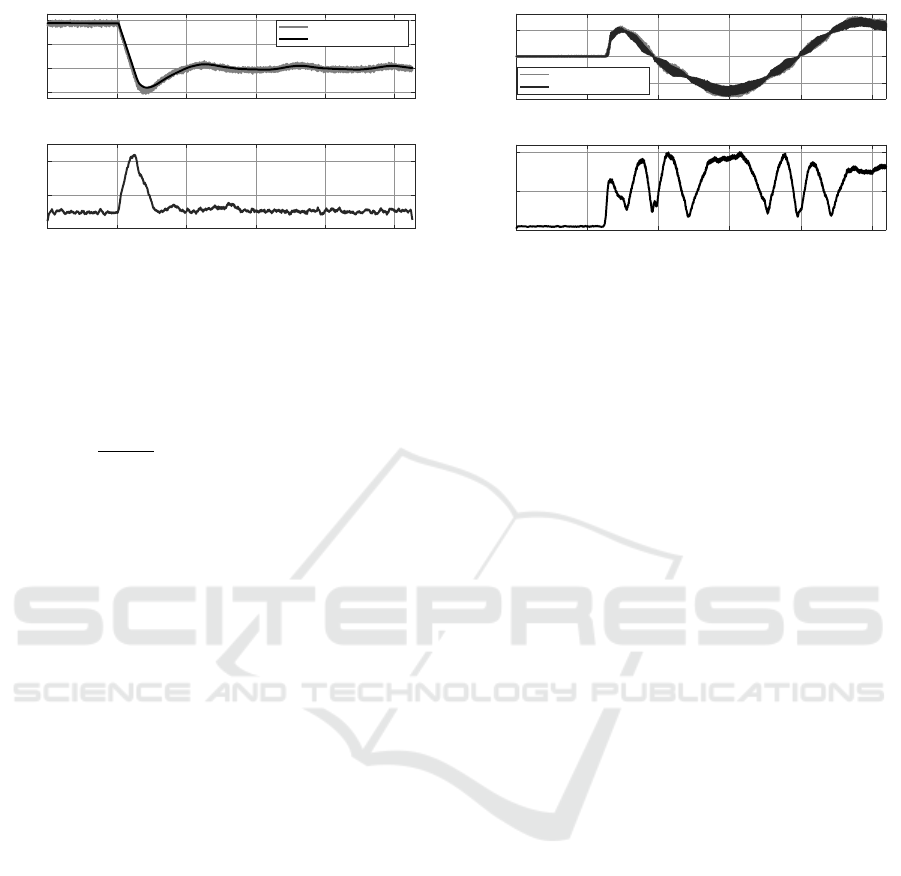
0 0.005 0.01 0.015 0.02 0.025
Time (s)
780
800
820
840
Voltage (V)
Output Voltage Vdc
Prototype measurement
Simulation data
0 0.005 0.01 0.015 0.02 0.025
Time (s)
0
2
4
Voltage (V)
Voltage Mean Error
Figure 14: (Up) Output voltage V
dc
from prototype mea-
surement and simulation data. (Down) Filtered absolute er-
ror between prototype and simulation voltage.
been performed on the absolute error according to
eq.23. A moving average over a window of 0.2ms
has been used :
ε
avg
[ j] =
1
2N + 1
+N
∑
k=−N
|
X
meas
[ j + k] − X
sim
[ j + k]
|
(23)
with N chosen as in eq.24 :
N · T
sampling
= 1 × 10
−4
s (24)
Fig.14 shows that prototype measurements is very
noisy. The error is up to 4.4V corresponding to the
minimum of Vdc. This difference corresponds to
some neglected losses which are not significant.
Fig.14 highlights that output voltage is not regu-
lated well at no load. However voltage stayed within
the +/ − 50V safety boundaries. This is acceptable
for no load condition.
Fig.15 shows the effects of coupling inductances
for both simulation and measures. Current ripple am-
plitude is varying from nearly 0A to 30A depend-
ing on the duty-cycle. As a consequence, currents
in boost inductances will enter Discontinuous Con-
duction Mode (DCM) at low power. In fact, stability
margins have been calculated with the hypothesis of
Continuous Conduction Mode (CCM) for all power.
Thus a stability analysis at DCM operation must be
performed for low power.
The mean error is oscillating between 2A and
10A. This error can be explained by the poor synchro-
nization of the high-frequency current oscillations be-
tween prototype measurement and simulation data.
That does not matter for this study.
Fig.15 doesn’t show a resonance around 10kHz, as
could be expected by analysis of section3.1. This can
be explained by the fact that damping parasitic param-
eters have been neglected. Thus resonance are well
damped in reality. Nevertheless, these resonances
have great chance to be excited. A known damping
has to be added to prevent this case to happen.
0 0.005 0.01 0.015 0.02 0.025
Time (s)
-50
0
50
Current (A)
Input Current Ia1
Prototype measurement
Simulation data
0 0.005 0.01 0.015 0.02 0.025
Time (s)
0
5
10
Current (A)
Current Mean Error
Figure 15: (Up) Input current I
a1
from prototype measure-
ment and simulation data. (Down) Filtered absolute error
between prototype and simulation current.
The differences are sufficiently low, which allows
to validate the model of C2IV.
5 CONCLUSIONS
Current loop stability study has highlighted that in-
put filter parameters of C2IV introduce potential res-
onances in the system and modify stability margins.
Although gain and phase margins are acceptable for
all operating points, delay margin is very low at low
power and at high input voltage. Adding a passive
damping is the preferred option to prevent oscillations
and move the margins to a more stable location.
Thus stability of the current loop of Vienna-type
rectifier has been proved on a wide range of operating
points. Weaknesses related to input filter have also
been identified.
Future work can improve stability study by using a
multi-variable approach, like H∞ methods with small
gain theorem and µ-analysis.
Stability of Discontinuous Conduction Mode is
another field of study. Coupled Inductances makes
this study a challenge for modelling current loop ade-
quately.
C2IV Rectifier show promising robustness perfor-
mance on all operating points. It can meet the increase
demand of pulsed power for Imaging Systems.
REFERENCES
COSTAN, V. (2007). Convertisseurs Parall
`
eles Entrelac
´
es :
Etude des Pertes Fer dans les Transformateurs Inter-
cellules. These de Doctorat, Institut National Poly-
technique de Toulouse.
Ji, C., Zhang, L., Zhao, R., Chen, B., Ming, Y., Xing, Y.,
and Ma, X. (2019). Dual-loop Control for Three-
phase Vienna Rectifier with Duty-ratio Feedforward.
ICINCO 2020 - 17th International Conference on Informatics in Control, Automation and Robotics
592

In IECON 2019 - 45th Annual Conference of the IEEE
Industrial Electronics Society, volume 1, pages 1715–
1720. ISSN: 1553-572X.
Kolar, J. W. and Friedli, T. (2011). The essence of three-
phase PFC rectifier systems. In 2011 IEEE 33rd In-
ternational Telecommunications Energy Conference,
pages 1–27.
Lai, R., Wang, F., Burgos, R., Boroyevich, D., Jiang, D.,
and Zhang, D. (2009). Average Modeling and Con-
trol Design for VIENNA-Type Rectifiers Considering
the DC-Link Voltage Balance. IEEE Transactions on
Power Electronics, 24(11):2509–2522.
Leibl, M. (2017). Three-Phase PFC Rectifier and High-
Voltage Generator for X-Ray Systems. Doctoral The-
sis, ETH Zurich.
Liu, a. J., Duan, a. B., and Zhang, C. (2017a). Independent
voltage outputs control for VIENNA rectifier consid-
ering multiple loads situations. In 2017 IEEE 3rd
International Future Energy Electronics Conference
and ECCE Asia (IFEEC 2017 - ECCE Asia), pages
1785–1790.
Liu, J., Ding, W., Qiu, H., Zhang, C., and Duan, B. (2017b).
A control scheme of the VIENNA rectifier with un-
balanced grid voltage. In 2017 Chinese Automation
Congress (CAC), pages 6263–6267.
Liu, T., Chen, C., Wang, T., Duan, S., and Cheng, H. (2018).
Proportional-Resonant Current Control for VIENNA
Rectifier in Stationary αβ Frame. In 2018 IEEE Inter-
national Power Electronics and Application Confer-
ence and Exposition (PEAC), pages 1–7.
Tang, X., Cao, Y., Xing, Y., Hu, H., and Xu, L. (2018). An
improved burst-mode control for VIENNA rectifiers
to mitigate DC voltage ripples at light load. In 2018
IEEE Applied Power Electronics Conference and Ex-
position (APEC), pages 1294–1298.
Current Loop Stability Analysis of a VIENNA-type Three-phase Rectifier for an Imaging System Power Supply Application
593
