
Mixed Pattern Recognition Methodology on Wafer Maps
with Pre-trained Convolutional Neural Networks
Yunseon Byun and Jun-Geol Baek
School of Industrial Management Engineering, Korea University, Seoul, South Korea
Keywords: Classification, Convolutional Neural Networks, Deep Learning, Smart Manufacturing.
Abstract: In the semiconductor industry, the defect patterns on wafer bin map are related to yield degradation. Most
companies control the manufacturing processes which occur to any critical defects by identifying the maps so
that it is important to classify the patterns accurately. The engineers inspect the maps directly. However, it is
difficult to check many wafers one by one because of the increasing demand for semiconductors. Although
many studies on automatic classification have been conducted, it is still hard to classify when two or more
patterns are mixed on the same map. In this study, we propose an automatic classifier that identifies whether
it is a single pattern or a mixed pattern and shows what types are mixed. Convolutional neural networks are
used for the classification model, and convolutional autoencoder is used for initializing the convolutional
neural networks. After trained with single-type defect map data, the model is tested on single-type or mixed-
type patterns. At this time, it is determined whether it is a mixed-type pattern by calculating the probability
that the model assigns to each class and the threshold. The proposed method is experimented using wafer bin
map data with eight defect patterns. The results show that single defect pattern maps and mixed-type defect
pattern maps are identified accurately without prior knowledge. The probability-based defect pattern classifier
can improve the overall classification performance. Also, it is expected to help control the root cause and
management the yield.
1 INTRODUCTION
The semiconductor manufacturing process is fine and
sophisticated. So, if a problem in any part of the
process occurs, it can be fatal on the yield. Yield
means the percentage of the actual number of good
chips produced, relative to the maximum number of
chips on a wafer. As the yield is the product quality
in the semiconductor industry, many engineers strive
to increase the yield.
One way to increase the yield is to check the
defect pattern on wafer bin maps and control the
causes of yield degradation. Wafer bin maps can be
obtained during the EDS(electrical die sorting) test.
EDS test is a step that checks the quality of each chip
on wafers. By testing various parameters such as
voltage, current, and temperature, the chips are
tagging good or bad. Then, engineers can identify
defect patterns that appear on the map. Defect
patterns contain various type such as center, donut,
scratch, and ring. Figure 1 shows the example of
pattern types on wafer bin maps. Each pattern is
related to the different causal factors. If the pattern is
exactly identified, it can be estimated what problem
occurs.
In fact, many engineers still check the map
visually (Park, J., Kim, J., Kim, H., Mo, K., and Kang,
P., 2018). So, it is difficult to identify many wafers
one by one as the demand for semiconductors
increases. Also, it is hard to classify the type,
especially when the patterns are mixed. Although
there are several studies for automatic classification,
more research on mixed patterns is still needed.
Figure 1: Various pattern types on wafer bin maps.
974
Byun, Y. and Baek, J.
Mixed Pattern Recognition Methodology on Wafer Maps with Pre-trained Convolutional Neural Networks.
DOI: 10.5220/0009177909740979
In Proceedings of the 12th International Conference on Agents and Artificial Intelligence (ICAART 2020) - Volume 2, pages 974-979
ISBN: 978-989-758-395-7; ISSN: 2184-433X
Copyright
c
2022 by SCITEPRESS – Science and Technology Publications, Lda. All rights reserved
The real data contains the maps that are difficult
to distinguish any pattern or many patterns are mixed
on a wafer. If the mixed-type defects are incorrectly
determined as a single-type defect, the causal factors
cannot be identified properly. This may affect any
critical defects and cause yield degradation. So,
accurate pattern classification is needed.
In this paper, we propose a pattern classification
method with a pre-trained convolutional neural
network model. The automatic classification method
based on the probabilities increases the overall
classification accuracy. Also, it helps to identify the
exact causes of defects and improve the yield.
The paper is organized as follows. Section 2
presents the related algorithms, and the proposed
method is explained in section 3. Section 4 presents
the experimental results on the wafer map image data
to verify the performance of the model. Finally,
section 5 describes the conclusion.
2 RELATED ALGORITHMS
Generally, the convolutional neural networks are
good at image processing. So, we use the
convolutional neural networks as a classifier. Before
classifying, the weights are learned by convolutional
autoencoders. These are utilized on the convolutional
neural networks to increase performance. In this
section, the convolutional autoencoder and the
convolutional neural networks are described.
2.1 Convolutional Autoencoder
The convolutional autoencoder is an unsupervised
learning model that learns features from images
without label information (Guo, X., Liu, X., Zhu, E.,
and Yin, J., 2017). When the number of data is small,
it can be overfitted for the training data by using the
supervised learning model. Then, it is more effective to
use an unsupervised learning method such as
autoencoder (David, O. E., & Netanyahu, N. S., 2016).
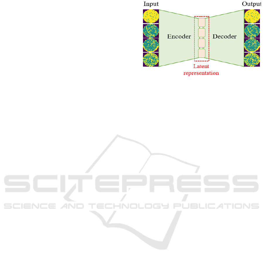
Autoencoder consists of an encoder and a
decoder, as shown in Figure 2. The key features are
trained in the hidden layer and the rest is lost in the
encoder. Then, the high dimensional data can be
reduced to the latent representations. A decoder
makes the approximation of the input as the output.
The output has to be close to the input as possible.
When as the number of nodes in the middle layer is
smaller than the number of nodes in the input layer,
the data can be compressed. The conventional
autoencoder represents high dimensional data as a
single vector.
Figure 2: The architecture of convolutional autoencoder.
The convolutional autoencoder, on the other
hand, compresses the data while maintaining the
coordinate space. So, it does not lose the space
information when the image data is used.
Convolutional autoencoder has the structure of
autoencoder using convolutional layers.
An encoder extracts the features from the
convolutional layers and pooling layers. The
convolutional layers find kernel patterns in the input
image. Kernels perform convolutional operations that
multiply the height and width of the images and
generate activation maps (Kumar, Sourabh, and R. K.
Aggarwal., 2018). And, the features are compressed
in the pooling layers. It helps to find important
patterns or reduce the number of computations (Park,
J., Kim, J., Kim, H., Mo, K., and Kang, P., 2018).
Max pooling is the most representative. An activation
map is divided by mn to extract the largest value.
Then, representative features can be extracted. After
the convolutional layers and pooling layers, the latent
representation
is generated in equation (1). is an
activation function for the input data . And, ∙ means
convolutional operation.
∙
(1)
A decoder reconstructs the data from the encoded
representation to be as close to the original input. The
reconstructed output value can be obtained from
equation (2).
means flip operation of weights and
c is biased.
∗
∈
(2)
The reconstruction loss measures how well the
decoder is performing and how close the output is to
the original data (Kumar, Sourabh, and R. K.
Aggarwal., 2018). The model is trained for
minimizing the reconstruction loss (Masci, J., Meier,
U., Ciresan, D., and Schmidhuber, J., 2011).
Mixed Pattern Recognition Methodology on Wafer Maps with Pre-trained Convolutional Neural Networks
975
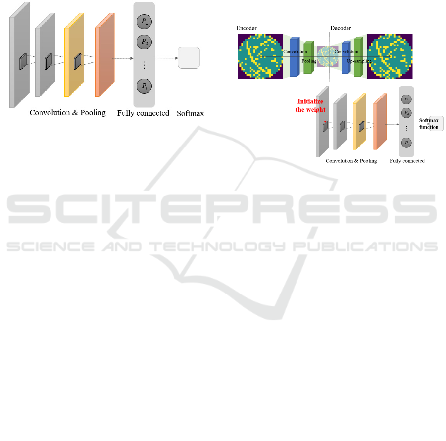
2.2 Convolutional Neural Networks
The convolutional neural networks are end-to-end
models that can be used on feature extraction and
classification. The hidden layers of CNNs consist of
convolutional layers, pooling layers, fully connected
layer, and output layer. The architecture is shown in
Figure 3.
Figure 3: The architecture of convolutional neural networks.
Features are extracted from convolutional layers
and pooling layers. After that, features are used for
classifying on a fully connected layer. Neurons in a
fully connected layer have full connections to all
activations in the previous layers. And, the number of
nodes in an output layer is the same as the number of
classes. On the output layer, the probabilities of classes
to be assigned are obtained using softmax function in
(3). The input data is .
means the weights of
node, and
means the bias of
node.
|,
,
∑
(3)
The loss function of the model in (4) can be
minimized using a backpropagation algorithm
(Cheon, S., Lee, H., Kim, C. O., and Lee, S. H., 2019).
The backpropagation algorithm looks for the
minimum error in weight space. The weights that
minimize the error is considered to be a solution to
the problem. is the number of data and is the
number of classes. And, 1
∈
is a function that has a
value of 1 when the actual class is .
1
1
∈
∈
(4)
The probabilities belonging to the
class are
obtained on the softmax function. And then, the node
with the highest probability value is classified into the
final class.
2.3 Pre-trained Convolutional Neural
Networks
The pre-trained convolutional neural networks is a
combination of convolutional autoencoder and
convolutional neural networks, as shown in Figure 4
(Masci, J., Meier, U., Ciresan, D., and Schmidhuber,
J., 2011). The weights of convolutional autoencoder
are used for initializing the weights of convolutional
neural networks.
Figure 4: The architecture of the pre-trained model.
The typical convolutional neural networks set the
initial weights randomly. On the other hand, using
weights of convolutional autoencoder make the data
be represented in low dimensional structures clearly.
It helps to create a classifier that reflects the features
more (Kumar, S., and Aggarwal, R. K., 2018).
3 THE PROPOSED METHOD
In the paper, we propose the pattern classification
method based on probabilities on softmax function.
The method contains three steps to classify the defect
patterns of wafer maps. The first step is to initialize
the weights with the convolutional autoencoder. The
second step is to create pre-trained convolutional
neural networks for single-type pattern classification.
The final step is to determine whether the patterns on
wafer maps are mixed based probabilities on softmax
function. Figure 5 shows the proposed method with
the pre-trained model.
3.1 Initialization of Weights with
Convolutional Autoencoder
Image data contains the coordinate information in pixel
units. The coordinate information of a defective die is
important. As the convolutional autoencoder preserves
ICAART 2020 - 12th International Conference on Agents and Artificial Intelligence
976
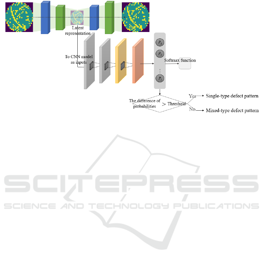
Figure 5: The proposed method.
all coordinate information of the inputs, it can prevent
distortion in the feature space. So, training with the
convolutional autoencoder is effective for extracting
the features of images (Masci, J., Meier, U., Ciresan,
D., and Schmidhuber, J., 2011).
3.2 Pre-trained Convolutional Neural
Networks Training
The convolutional neural networks are known for the
classifier which has high performance on image data.
It uses the softmax function to classify classes.
Softmax is one of the activation functions. It takes
extracted features as inputs and calculates the
probabilities on each class. The sum of probabilities
is 1. And then, a class that has the highest probability
becomes the result of classification.
To get the probabilities of each class, we train the
convolutional neural networks with the single-type
pattern data. Then, the weights trained with the
convolutional autoencoder are set to the initialized
value of convolutional neural networks. It makes the
weights be finely adjusted and key information is
preserved. So, the features of the images are well-
reflected. Also, the pre-trained model is effective when
the number of labeled data is small (Kohlbrenner, M.,
Hofmann, R., Ahmmed, S., and Kashef, Y., 2017).
3.3 Probabilistic Mixed-type Pattern
Recognition on Wafer Maps
The model can obtain the probabilities on softmax
function. And, the class that the highest probability is
assigned becomes the result for classification. If there
are single-type defects, the probability of certain node
is prominent. However, for mixed-type patterns, there
are the several highest probabilities, so the difference
in maximum and next maximum is not large. The
calculation between the difference of probabilities
and a threshold in (5) is used for determining whether
the patterns are mixed or not. The prob
∈
means the probability that belongs on the class .
threshold
maximum
prob
∈
Nextmaximum
prob
∈
(5)
If the difference of probabilities is large, it means
that the pattern type of wafer map is clearly single.
And, if the difference is not large, it means that the
pattern type is mixed. The threshold value is specified
after checking the probability distribution of data.
4 THE EXPERIMENTAL RESULT
The dataset used in the experiment is WM-811K. It
contains 172,950 wafer map images. Each pixel in the
image represents a die on wafer maps. After testing, the
normal chip is represented as 1, and the defective chip
is represented as 2. Although the shape of the wafer is
a circle, the inputs of the convolutional neural network
have to be square. So, the empty pixel is represented as
0. The goal of the experiment is to classify the
defective patterns. So, we consider the only failure
types, not normal or no label. The number of usable
data is 25,519 but the size of all images is not the same.
Most of them are rectangular. Then, we resize the data
to the 2626 square images for the training of CNNs.
Mixed Pattern Recognition Methodology on Wafer Maps with Pre-trained Convolutional Neural Networks
977
Finally, we use only 7,915 to train the model, and the
data is divided into 7:3 and used for training and testing.
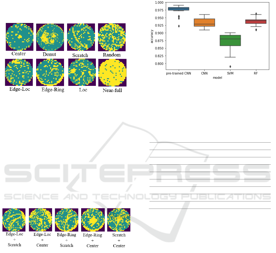
The inputs consist of eight single-type pattern
data, shown in Figure 6. There are center, donut,
scratch, random, edge-loc, edge-ring, loc, near-full.
Figure 6: The single-type defect pattern maps.
The data given contains only single-type defect
patterns. In this study, the recognition of mixed-type
defect patterns requires the mixed-type data on wafer
maps. We generated the mixed-type patterns through
the computation of single-type patterns. The target
patterns for generation are center, scratch, edge-loc,
and edge-ring patterns. We assume that only two
single-type patterns can be mixed. The generated
patterns are the mixture of edge-loc and scratch, the
mixture of edge-loc and center, the mixture of edge-
ring and scratch, the mixture of edge-ring and center,
and the mixture of scratch and center as shown in
Figure 7. The number of generated data is 580.
Figure 7: The mixed-type defect pattern maps.
4.1 The Result for Single-type Pattern
Classification
The pre-trained model is used for classifying the
single-type pattern maps to calculate the sigmoid
probability value. Figure 8 shows the 10-fold
classification performance of models. Compared with
the machine learning method like support vector
machine and random forest, the performance of the
pre-trained convolutional neural networks is excellent.
In particular, the proposed model outperformed the
original convolutional neural networks. This shows
that the setting of the initial weights, which reflect the
data characteristics using a convolutional autoencoder,
helps better classification of the patterns.
Figure 8: Classification performance of models.
The following Table 1 shows the result for
classification with the single-type test cases. Overall
classification accuracy is high, but the accuracy of
scratch, edge-loc, loc patterns is relatively low.
Table 1: Classification accuracy for the single-type data.
Pattern Type Accuracy
Center 97%
Donut 100%
Scratch 85.5%
Random 90%
Edge-Loc 87%
Edge-Ring 98.5%
Loc 85.4%
Near-full 100%
4.2 The Result for Mixed-type Pattern
Classification
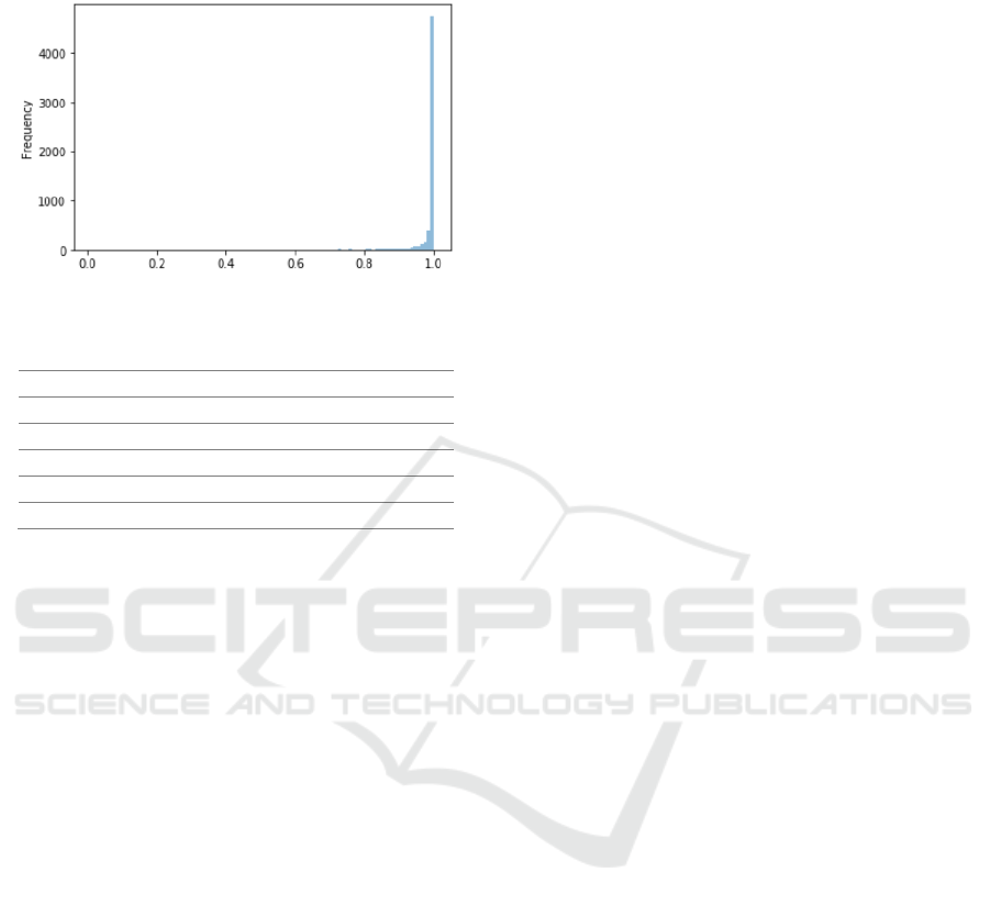
The defect pattern maps can be determined whether
the patterns are mixed or not by calculating between
the threshold and the difference of probabilities on
softmax function. Then, the value of the threshold is
obtained from the distribution of probabilities on
softmax. Figure 9 describes the histogram of
probabilities. In the figure, the value is determined to
0.96 empirically.
By calculating the threshold and the difference of
probabilities, the mixed-type patterns can be
recognized. Table 2 shows the testing result of the
mixed-type data. In these results, we judge that the
model classified correctly only if it recognizes the
mixed-type pattern and accurately detects which one
is mixed. Although the model is well-determined for
mixing, it was not good for detecting a single-type
pattern that constitutes a mixed-type pattern. Among
ICAART 2020 - 12th International Conference on Agents and Artificial Intelligence
978
them, the accuracy is relatively low when an edge-
ring pattern is mixed.
Figure 9: The histogram for the difference of probabilities.
Table 2: Classification accuracy for the mixed-type data.
Pattern Type Accuracy
Center + Edge-Loc 59%
Scratch + Edge-Loc 41.6%
Center + Edge-Ring 69%
Scratch + Edge-Ring 64.4%
Center + Scratch 40%
5 CONCLUSIONS
This paper proposed the probabilistic method for
classifying defect patterns on wafer bin maps. We
construct the pre-trained model with the convolutional
autoencoder and convolutional neural networks. And,
we determine whether the patterns are mixed on wafer
maps, by calculating between the threshold and the
difference of probabilities. Experiments with WM-
811K data verifies the performance of the model. The
classification performance for the single-type pattern
of the model is excellent, but the performance for the
mixed-type pattern is relatively low. It is assumed that
the patterns of training data are not clearly
distinguished and that the threshold value is set to a
very high value due to the imbalance in the number of
single-type data and mixed-type data. So, it is
necessary to supplement such parts later. And, we
assume the only two patterns can be mixed, so the
study for more mixed-type patterns has to be conducted
to apply for the actual data.
ACKNOWLEDGEMENTS
This work was supported by the National Research
Foundation of Korea (NRF) grant funded by the Korea
government (MSIT) (NRF-2019R1A2C2005949).
This work was also supported by the BK21 Plus (Big
Data in Manufacturing and Logistics Systems, Korea
University) and by the Samsung Electronics Co., Ltd.
REFERENCES
Cheon, S., Lee, H., Kim, C. O., & Lee, S. H., 2019.
Convolutional Neural Network for Wafer Surface
Defect Classification and the Detection of Unknown
Defect Class. IEEE Transactions on Semiconductor
Manufacturing, 32(2), 163-170.
David, O. E., & Netanyahu, N. S., 2016. Deeppainter:
Painter classification using deep convolutional
autoencoders. In International conference on artificial
neural networks (pp. 20-28). Springer, Cham.
Guo, X., Liu, X., Zhu, E., & Yin, J., 2017. Deep clustering
with convolutional autoencoders. In International
Conference on Neural Information Processing (pp. 373-
382). Springer, Cham.
Kim, H., & Kyung, G., 2017. Wafer Map defects patterns
classification using neural networks. Korean Institute of
Industrial Engineers, 4319-4338.
Kohlbrenner, M., Hofmann, R., Ahmmed, S., & Kashef, Y.,
2017. Pre-Training CNNs Using Convolutional
Autoencoders.
Kumar, S., & Aggarwal, R. K., 2018. Augmented
Handwritten Devanagari Digit Recognition Using
Convolutional Autoencoder. In 2018 International
Conference on Inventive Research in Computing
Applications (ICIRCA) (pp. 574-580). IEEE.
Masci, J., Meier, U., Cireşan, D., & Schmidhuber, J., 2011.
Stacked convolutional auto-encoders for hierarchical
feature extraction. In International Conference on
Artificial Neural Networks (pp. 52-59). Springer,
Berlin, Heidelberg.
Nakazawa, T., & Kulkarni, D. V., 2018. Wafer map defect
pattern classification and image retrieval using
convolutional neural network. IEEE Transactions on
Semiconductor Manufacturing, 31(2), 309-314.
Park, J., Kim, J., Kim, H., Mo, K., & Kang, P., 2018. Wafer
Map-based Defect Detection Using Convolutional
Neural Networks. Journal of the Korean Institute of
Industrial Engineers, 44(4), 249-258.
Wu, M. J., Jang, J. S. R., & Chen, J. L., 2014. Wafer map
failure pattern recognition and similarity ranking for
large-scale data sets. IEEE Transactions on
Semiconductor Manufacturing, 28(1), 1-12.
Mixed Pattern Recognition Methodology on Wafer Maps with Pre-trained Convolutional Neural Networks
979
