
Antimonide-based Superlattice Infrared Barrier Photodetectors
U. Zavala-Moran
1
, R. Alchaar
2
, J. P. Perez
2
, J. B. Rodriguez
2
, M. Bouschet
2
, V. H. Compean
1
,
F. de Anda
1
and P. Christol
2
1
IICO, UASLP, San Luis Potosí, Mexico
2
IES, Univ. Montpellier, CNRS, Montpellier, France
Keywords: Infrared Quantum Detector, Barrier Structure, Sb-based Heterostructure, Type-II Superlattice.
Abstract: Barrier structures are now the design of high performance antimonide-based (Sb-based) cooled infrared (IR)
quantum detectors. In this communication, we report on electrical and electro-optical characterizations of Ga-
free and Ga-containing type-II superlattices (T2SL) photodetectors structures grown by Molecular Beam
Epitaxy (MBE). Experimental measurements on Ga-free XBn and Ga-containing XBp samples were made by
photo-response measurements and dark current density-voltage (J-V) characteristics performed on detectors
as a function of temperature. Identification of bias voltage characteristics were extracted from measurements
and resulting dark current values were compared to the state of the art of infrared technology.
1 INTRODUCTION
In order to reduce the dark current, and therefore the
noise of the device, the first infrared (IR) barrier
detector was proposed by A. White in 1983 (White,
1983). He proposed an architecture device composed
of isotype (n-type) heterostructures where a high band
gap energy barrier layer was placed between the
absorbing and contact layers of smaller gap materials.
As the objective of the barrier layer is to block the
majority carriers (in this case electrons) while
allowing the photogenerated minority carriers (holes)
to reach the contact layer, he called this device "high
impedance photoconductor". However, at that time,
obtaining a very low or zero valence band offset was
difficult to achieve with the main IR detection
materials based on InSb and HgCdTe (MCT).
Everything changed in the mid-2000s with the
demonstration of the InAs-based barrier structure by
Maimon and Wicks (Maimon, 2006) and then
accelerated with the used of antimonide-based (Sb-
based) materials, such as InAsSb (Klipstein, 2011)
and type II superlattice (T2SL) structures lattice
matched to GaSb substrate (Klipstein, 2015), to build
IR barrier photodetectors.
Barrier structures are now the standard for the
design of Sb-based cooled IR photodetectors. Such
high-performance detector structure, which replaced
the usual pin photodiode, is made of n-type or p-type
photon absorbing layer, a barrier layer B and a contact
layer X that can be made from either the same, or a
different material, to that used for the photon
absorbing layer. Consequently, these quantum
detectors are named XBn or XBp structures, also
called bariodes.
Specialist of IR photonic Sb-based devices
fabricated by Molecular Beam Epitaxy (MBE) on
GaSb substrate, the Institute of Electronic and
Systems (IES) of the University of Montpellier
(France) has studied T2SL quantum detectors
dedicated to IR spectral domain since several years
(Rodriguez, 2005, Jaworowicz, 2010, Delmas, 2014).
This paper reports electro-optical and electrical
experimental measurements performed on Ga-free
InAs/InAsSb and Ga-containing InAs/GaSb T2SL
structures, grown by MBE, in XBn and XBp
photodetector configurations, respectively.
2 T2SL XBN AND T2SL XBP
BARRIER STRUCTURES
2.1 Advantages of Barrier Structure
To understand the advantages of the barrier detector,
is necessary to compare it with the pn junction
photodiode.
In the pn junction structure with reverse bias
applied, the presence of the space charge zone on
either side of the p/n interface blocks the transport of
Zavala-Moran, U., Alchaar, R., Perez, J., Rodriguez, J., Bouschet, M., Compean, V., de Anda, F. and Christol, P.
Antimonide-based Superlattice Infrared Barrier Photodetectors.
DOI: 10.5220/0009004900450051
In Proceedings of the 8th International Conference on Photonics, Optics and Laser Technology (PHOTOPTICS 2020), pages 45-51
ISBN: 978-989-758-401-5; ISSN: 2184-4364
Copyright
c
2022 by SCITEPRESS – Science and Technology Publications, Lda. All rights reserved
45
the majority carriers and allows the transfer of the
minority ones. However, this zone with electric field
generates Shockley-Read-Hall (SRH) recombination
darkness current, thus generation-recombination
(GR) current, which may be important in the IR
spectral domain. Dark current of IR photodiodes,
such as InSb, is dominated by SRH current at its
operating temperature (~80K).
The main objective of the XBn or XBp barrier
structure is to reduce the contribution of the SRH
current to the dark current of the detector. For that, it
is required to control the electric field zone by
confining it in the high band gap barrier material
instead of in the absorbing zone structure. Then, SRH
processes occur in the high band gap material, not in
the IR absorbing layer. In addition, the barrier layer
plays the same role as the space charge zone in the pn
structure as blocking the majority carriers and
allowing the flow of the minority ones.
Consequently, when the barrier detector structure
is correctly designed, GR dark current is strongly
reduced, even eliminated, and the performances of the
photodetector are improved (Klipstein, 2015).
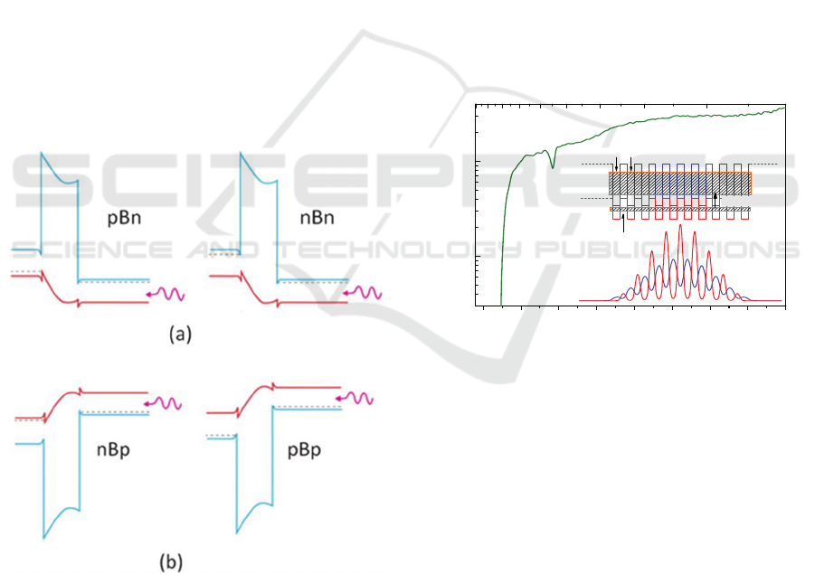
Figure 1 shows the possible XBn and XBp
designs.
Figure 1: Schematic view of XBn (a) and XBp (b)
structures. In each case, the contact layer (X) is on the left
and the IR absorbing layer (n or p) is on the right (according
to (Klipstein, 2015)).
2.2 T2SL Structures
The type-II superlattice (T2SL) was proposed at the
end of the 80's as a material for IR detection (Smith,
1987).
A superlattice is a stack of periodic layers whose
thickness is of the order of a few nanometers. It is an
artificial quantum structure composed of coupled
multi-quantum wells. Carriers (electrons and holes)
are then confined into energy minibands and optical
absorption occurs between two of these minibands.
In the case of Sb-based materials, such quantum
structure presents particular type-II band alignment
where the carriers are confined in the adjacent
materials (Figure 2) and, depending on the thickness
layers, the fundamental valence to conduction (V1-
C1) interminiband absorption (detector cut-off
wavelength λ
c
) can address all the thermal IR, from 3
to 30μm (Wei, 2004).
Figure 2 shows a Ga-containing InAs/GaSb T2SL
fundamental absorption spectrum at T= 300K.
Figure 2: T2SL absorption coefficient extracted from room
temperature absorption spectrum. In the inset, band
diagram and probability densities of fundamental C1 and
V1 levels of first electron and heavy hole (hh) minibands
are reported.
3 T2SL XBN AND T2SL XBP
DETECTORS: FABRICATION
AND CHARACTERIZATION
Lattice-matched to the GaSb substrate, the absorbing
zone is composed of strain compensated Ga-free
InAs/InAsSb or Ga-containing InAs/GaSb T2SL,
operating in the MWIR (midwave infrared 3-5µm) to
LWIR (longwave infrared 8-12µm) spectral domains,
respectively.
0.20 0.25 0.30 0.35 0.40 0.45 0.50 0.55 0.60
100
1000
Wavelength (µm)
f
v
2
f
e
2
I<f
C1
If
V1
>I
2
= 60%
GaSb
InAs
First electron
miniband
First hole
miniband
absorption coefficient (cm
-1
)
Energie (eV)
T = 300K
Absorption
T2SL structure
6.5 6 5.5 5 4.5 4 3.5 3 2.5
PHOTOPTICS 2020 - 8th International Conference on Photonics, Optics and Laser Technology
46
3.1 Ga-free T2SL XBn Photodetector
The XBn detector operating in the MWIR domain is
made of 1µm-thick non-intentionally doped (nid) n-
type Ga-free InAs/InAs
0.69
Sb
0.31
T2SL absorbing layer,
80nm-thick p-doped AlAs
0.09
Sb
0.91
barrier layer and
100nm-thick n
+
-doped InAs/InAs
0.69
Sb
0.31
T2SL
contact layer (Figure 3). Equivalent Ga-free structure
has recently been fabricated on Si substrate (Durlin,
2019)
Figure 3: Schematic cross-section of the Ga-free T2SL XBn
photodetector on GaSb substrate.
Figure 4 displays the high-resolution x-ray
diffraction (HRXRD) spectrum of the T2SL XBn
structure grown by MBE on 2” (100) GaSb substrate.
The presence of numerous and intense satellite peaks
is a signature of the crystallographic structure’s quality
and their positions allow to calculate the InAs/InAsSb
period thickness of the T2SL stacking equal to 4.40
nm.
26 27 28 29 30 31 32 33 34 35
10
0
10
1
10
2
10
3
10
4
10
5
10
6
Intensity (cts/s)
Ω/2Θ(°)
T2SL period = 4.40 nm
Figure 4: High-resolution X-ray diffraction patterns of Ga-
free T2SL InAs (3.30nm)/InAs
0.69
Sb
0.31
(1.10nm) structure
on GaSb substrate.
From epitaxial SL material, circular mesa
photodiodes were fabricated using standard
photolithography with a mask set containing diodes
and photodiodes with several diameters, from 60µm up
to 310µm (figure 5). Mesa photodiodes were realized
by wet etching using citric acid solution and
polymerized photoresist was used to protect the mesa
surface from ambient air. Metallization were ensured
on the n-GaSb substrate and on the n-type T2SL cap
layer. Next, the devices are mounted in a cryogenic
probe station to perform dark current density-voltage
(J-V) measurements.
Figure 5: Top view of a processed sample, blind diodes (C)
and photodiodes (P) with several diameters from 60µm up to
310µm.
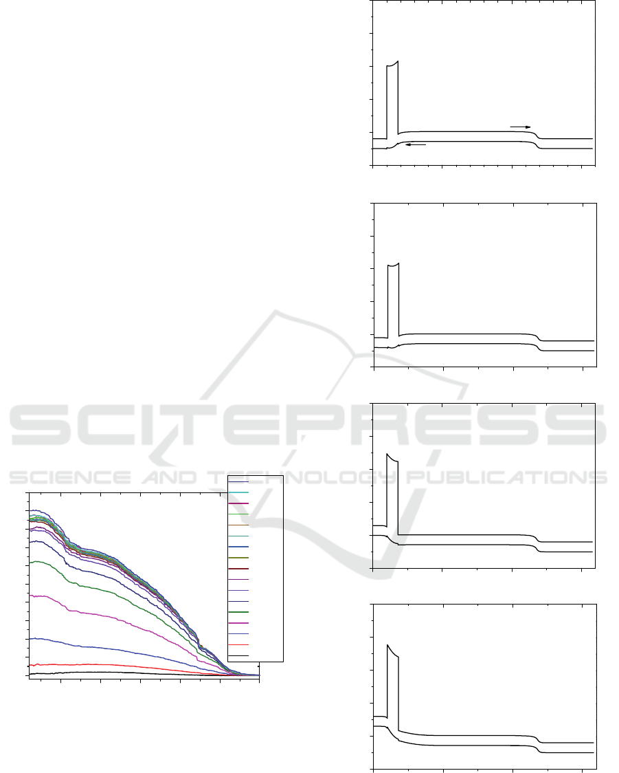
Figure 6 shows the J-V curves at temperatures
ranging from 77 to 250K, performed on a detector with
a 210 µm-diameter. At low temperature, until 110K,
the dark current is limited by the photonic current due
to the experimental set-up (probe station).
The shapes of the dark J(V) characteristics are in
accordance with the those obtained with XBn Ga-free
MWIR diodes, reported elsewhere (Baril, 2016 ; Ting,
2018).
-1.4 -1.2 -1.0 -0.8 -0.6 -0.4 -0.2 0.0 0.2 0.4
10
-10
10
-9
10
-8
10
-7
10
-6
10
-5
10
-4
10
-3
Density current (A/cm
2
)
Bias (V)
77K
90K
110K
120K
130K
135K
140K
145K
150K
155K
160K
165K
170K
180K
190K
200K
220K
250K
Ga-free T2SL XBn MWIR detector
residual photonic current
Figure 6: Dark current density-voltage (J-V) characteristics
at different temperatures, from 77 to 250K, of a Ga-free
T2SL XBn MWIR detector.
Antimonide-based Superlattice Infrared Barrier Photodetectors
47
In the forward positive bias, the low dark current
is due to the thin n-type top contact layer compared to
the absorbing layer (100 nm vs 1µm). A slight
negative bias applied to the top contact layer
(typically - 200mV) is necessary for the device
operation.
At temperature lower than 180K, the slope of the
dark currents plots between -0.1V and -0.4V shows
the presence of GR current, indicating that the device
design must be optimised. At higher temperature, one
can see that the slope is reduced as diffusion current
becomes dominant in the dark current.
At the expected operation temperature equal to
150K, dark current density as low as 2x10
-6
A/cm
2
, at
typical bias operation equal to -200mV, is extracted.
Lower dark current could be obtained by a better
control of targeted doping values of MBE grown
layers.
The samples were then wire bounded onto a 68
pin LCC and placed in a liquid nitrogen cryostat in
order to perform non-calibrated photoresponse (PR)
measurements by using a Nicolet-870 Nexus Fourier
transform infrared (FTIR) spectrometer with non-
calibrated IR source. Figure 7 shows the front side
illuminated uncalibrated PR spectra obtained at
different biases and at T = 150K. One can observe a
50% cut-off wavelength at 4.2µm and that the
collected signal begins to saturate at bias applied
equal to -220mV.
2.5 3.0 3.5 4.0 4.5 5.0
Ga-free T2SL XBn MWIR detector
Uncalibrated photoresponse spectra (a.u)
Wavelength(µm)
-1.5V
-1V
-800mV
-500mV
-400mV
-350mV
-300mV
-280mV
-260mV
-240mV
-220mV
-200mV
-180mV
-160mV
-140mV
-120mV
-100mV
T = 150K
bias applied
Figure 7: Uncalibrated PR spectra recorded at T= 150K, for
different biases applied from -100 to 1500mV, of a Ga-free
T2SL XBn MWIR detector.
To explain the behaviour of the PR spectrum as a
function of bias applied, band diagrams of the XBn
device are calculated at T= 150K and reported in
0.00.51.01.5
-1
0
1
2
3
4
Energy (eV)
Position (µm)
T = 150K
V
bias
= 0V
Ga-free T2SL XBn MWIR detector
a)
Barrier
Layer
Contact Layer
Absorbing Layer
é
hh
0.0 0.5 1.0 1.5
-1
0
1
2
3
4
Contact Layer
b)
Energy (eV)
Position (µm)
Ga-free T2SL XBn MWIR detector
T = 150K
V
bias
= -100mV
Barrier
Layer
Absorbing Layer
0.0 0.5 1.0 1.5
-1
0
1
2
3
4
Energie (eV)
Position (µm)
c)
Ga-free T2SL XBn MWIR detector
T = 150K
V
bias
= -500mV
Absorbing Layer
Barrier
Layer
Contact
Layer
0.0 0.5 1.0 1.5
-1
0
1
2
3
4
Energie (eV)
Position (µm)
d)
Ga-free T2SL XBn MWIR detector
T = 150K
V
bias
= -800mV
Absorbing Layer
Barrier
Layer
Contact
Layer
Figure 8: Calculated band diagrams using the ATLAS
software from SILVACO (Abautret, 2013) of the Ga-free
XBn barrier structure at 150K and 0V (a), -100mV (b), -
500mV (c), and -800mV (d).
PHOTOPTICS 2020 - 8th International Conference on Photonics, Optics and Laser Technology
48
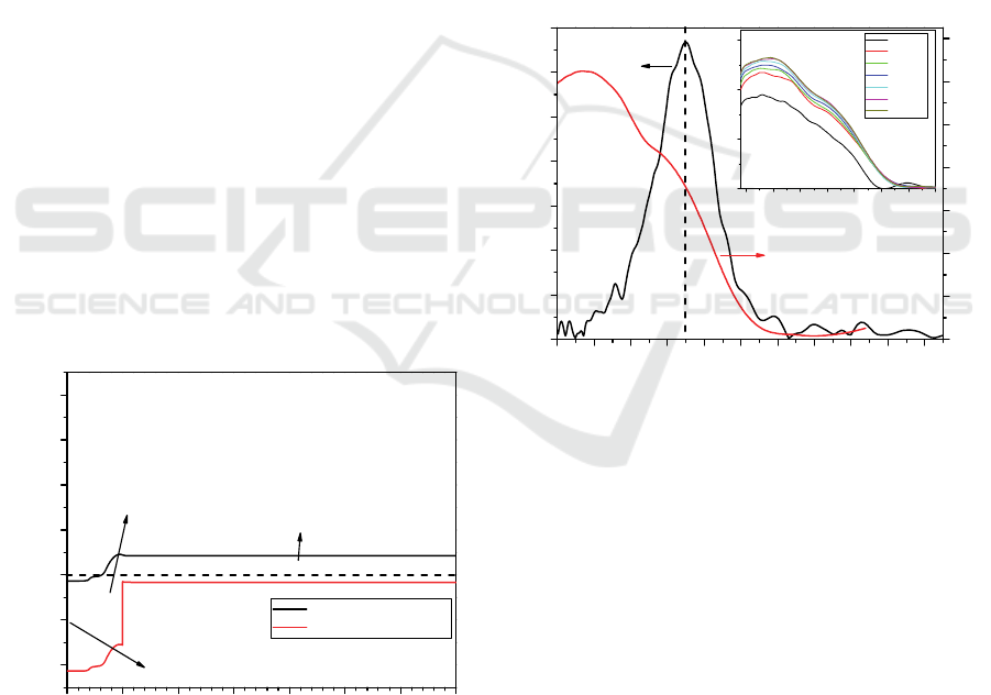
Figure 8 for four typical bias voltages (V
bias
= 0V,
V
bias
= -100mV, V
bias
= -500mV, V
bias
= -800mV).
At V
bias
= 0V, the band diagram highlights the
presence of a potential barrier blocking the minority
heavy hole carriers. Even, at bias operation equal to -
100mV, this potential barrier remains, penalizing the
quantum efficiency (Figure 7).
At V
bias
= -500mV, the bias is high enough to
suppress the potential barrier allowing the transport
of hole minority carrier to the top contact layer. The
maximum of PR is collected.
3.2 Ga-containing T2SL XBp
photodetector
In this part, another kind of barrier structure is
considered. It is a Ga-containing InAs/GaSb T2SL
XBp detector operating in the LWIR domain.
To maximize the quantum efficiency, the Ga-
containing T2SL is p-type doping (Giard, 2014).
Consequently, the electrons are the minority carriers
and the barrier, made of InAs/AlSb T2SL (Delmas,
2017), is tailored to have a large offset in the valence
band and minimal offset in the conduction band,
therefore blocking majority holes and collecting
photo-generated electrons.
The XBp detector structure under consideration is
made of lightly p-type doped 3.2µm thick InAs/GaSb
T2SL absorbing layer, a heavily n-type doped wide
bandgap InAs/GaSb T2SL and a lightly n-type doped
InAs/AlSb barrier layer. Figure 9 shows the
calculated band diagram at 80K and under no bias.
0.0 0.5 1.0 1.5 2.0 2.5 3.0 3.5
-0.4
-0.2
0.0
0.2
0.4
0.6
0.8
Ga-containing T2SL XBp LWIR detector
InAs/GaSb T2SL
Absorbing Layer
InAs/AlSb T2SL
Barrier Layer
Energy (eV)
Position (µm)
Conduction band edge
Valence band edge
E
f
T= 80K
V
bias
= 0 V
InAs/GaSbT2SL
Contact Layer
Figure 9: Calculated band diagram of the Ga-containing
XBp barrier structure at 80K and 0V.
In addition of the photoluminescence (PL)
spectrum, figure 9 displays the non-calibrated photo-
response (PR) spectrum at V
bias
= -100mV for a
detector device having a 90 µm-diameter. The 50%
cut-off wavelength equal to 10.5µm for the spectral
PR corresponds to the PL peak, in agreement with the
targeted value suitable for LWIR applications. The
inset shows the PR measurements at different biases
and the PR starts to saturate after -50mV bias applied,
enough to reduce the possible conduction potential
barrier (Figure 9). Measured elsewhere (Höglund,
2018), the detector quantum efficiency (without anti-
reflection coating) reaches 35% at 80K. Figure 11a
reports normalized PR values extracted from the PR
measurements (inset Figure 11) at different biases and
at 10.5µm.
Dark current density-voltage measurement (J-V)
is also performed at 80K. J
dark
result is shown in
Figure 11b and the associated differential resistance
area product R
d
A is reported in Figure 11c (R
d
is
calculated from the derivative of the voltage over the
current and A is the device area).
7 8 9 1011121314151617
7 8 9 10 11 12 13 14
Photoresponse (a.u)
Wavelength (µm)
-25 mV
-50 mV
-75 mV
-100 mV
-150 mV
-200 mV
-300 mV
T=80K
Wavelength (µm)
PL intensity (a.u)
10.5 µm
Photoresponse (a.u)
T = 80K
Figure 10: PL and PR (at V
bias
= -100mV) measurements at
80K of a Ga-containing XBp T2SL detector device. The
inset shows the PR at different biases.
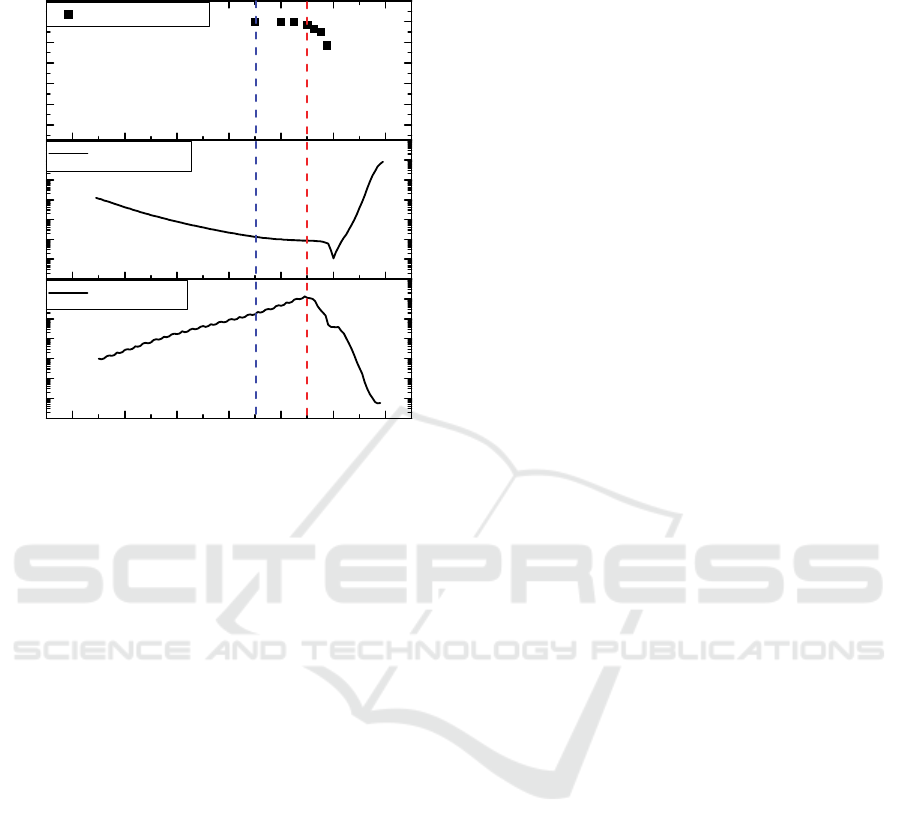
The shape of the curves displayed in Figure 11,
help us to identify the two main dark current regimes
of the LWIR detector. First, the operating bias V
op
.= -
100mV. At this bias, the device is fully turned on
(where R
d
A is at a maximum value), the diffusion
plateau is reached, and the PR value saturates. The
depletion region is still confined within the barrier.
Next, the V
GR
= -300 mV. At this bias, GR current
starts to dominate the dark current of the diode, the
barrier is fully depleted, and the depletion region
reaches the absorbing region.
From this analysis, it is possible to identify the
operating bias of the device, which is -100mV. At this
voltage, dark current density value as low as 8x10
-4
A/cm
2
and R
d
A product as high as 1160 Ω.cm
2
are
extracted at T = 80K.
Antimonide-based Superlattice Infrared Barrier Photodetectors
49
10
-3
10
-1
10
1
10
3
10
-5
10
-3
10
-1
10
1
0.0
0.2
0.4
0.6
0.8
1.0
1.2
-1.0 -0.8 -0.6 -0.4 -0.2 0.0 0.2
-0.2-0.4
-0.6
-0.8
-1.0
0.0
V
op
=-100 mVV
GR
=-300 mV
0.2
Voltage (V)
R
D
A (Ω.cm²)
T=80K
T=80K
J
dark
(A/cm²)
c)
b)
Normalized PR
a)
T=80K
Figure 11: Experimental characterizations of a Ga-
containing XBp T2SL detector device. From top to bottom :
(a) normalized PR, (b) dark current density J
dark
, (c)
differential resistance area product (R
d
A) as a function of
the voltage at T = 80K. Two particular bias are identified :
The operating bias V
op
and the V
GR
bias for which the G-R
current begins to dominate the dark current of the diode.
4 CONCLUSIONS
InAs/InAsSb Ga-free XBn T2SL MWIR and
InAs/GaSb Ga-containing XBp T2SL LWIR
quantum detectors have been fabricated and
characterized.
These photodetectors showed cut-off wavelength
around 4.2µm at 150K and 10.5µm at 80K,
respectively. Dark current density values, extracted
from J(V) measurements, are equal to 2x10
-6
A/cm
2
at 150K for the Ga-free device and 8x10
-4
A/cm
2
for
the Ga-containing one.
Compared to the state of the art (i.e; the Rule 07
(Tennant, 2008)), these values are from two to one
decades higher, respectively. Concerning the Ga-free
T2SL, such result is due to the presence of GR dark
current at operating bias. Improvement in the design
and on the control of doping layers during the MBE
growth are necessary to suppress this behaviour and
will be the subject of forthcoming studies. For the Ga-
containing T2SL, the origin of high dark current is
different. The current of the device is dominated by
diffusion current at operating bias but the
performance is penalized by the well-known poor
lifetime value of minority carriers in Ga-containing
T2SL (Svensson, 2011). A solution would be the
development of Ga-free T2SL quantum detector
structure dedicated for the LWIR spectral domain.
ACKNOWLEDGEMENTS
This work was partially funded by the French
“Investment for the Future” program (EquipEx
EXTRA, ANR 11-EQPX-0016), by the ESA contract
number 4000116260/16/NL/BJ and by the French
ANR under project HOT-MWIR (N° ANR-18-CE24-
0019-01).
REFERENCES
Abautret, J., Perez, J.P., Evirgen, A., Martinez, F., Christol,
P., Fleury, J., Sik, H., Cluzel, R., Ferron, A., Rothman,
J., 2013. Electrical modeling of InSb PiN photodiode
for avalanche operation, Journal of Applied Physics,
113, 183716.
Baril, N., Brown, A., Maloney, P., Tidrow, M., Lubyshev,
D., Qui, Y., Fastenau, J.M., Amy W. K. Liu, A.W.K.,
Bandara, S., 2016. Bulk InAsSb nBn photodetectors
with greater than 5lm cutoff on GaSb, Applied Physics
Letters, 109, 122104
Delmas, M., Rodriguez, J.B., Christol, P., 2014. Electrical
modeling of InAs/GaSb superlattice mid-wavelength
infrared pin photodiode to analyze experimental dark
current characteristics, Journal of Applied Physics, 116,
113101
Delmas, M., Rossignol, R., Rodriguez, J.B., Christol, P.,
2017. Design of InAs/GaSb superlattice infrared barrier
detectors, Superlattices and Microstructures, 104, 402.
Durlin, Q., Perez, J.P., Cerutti, L., Rodriguez, J.B., Cerba,
T., Baron, T., Tournie, E., Christol, P., 2019. Midwave
infrared barrier detector based on Ga-free InAs/InAsSb
type-II superlattice grown by molecular beam epitaxy
on Si substrate, Infrared Physics & Technology 96, 39
Giard, E., Ribet-Mohamed, I., Jaeck, J., Viale, T., Haïdar,
R., Taalat, R., Delmas, M., Rodriguez, J.B., Steveler,
E., Bardou, N., Boulard, F., Christol, P., 2014.
Quantum efficiency investigations of type-II
InAs/GaSb midwave infrared superlattice
photodetectors, Journal of Applied Physics, 116,
043101.
Höglund, L., Rodriguez, J.B., Marcks von Würtemberg, M.,
Naureen, S., Ivanov, R., Asplund, C., Alchaar, R.,
Christol, P., Rouvié, A., Brocal, J., Saint-Pé, O.,
Costard, E., 2018. Influence of shallow versus deep
etching on dark current and quantum efficiency in
InAs/GaSb superlattice photodetectors and focal plane
PHOTOPTICS 2020 - 8th International Conference on Photonics, Optics and Laser Technology
50

arrays for long wavelength infrared detection, Infrared
Physics & Technology 95, 158.
Jaworowicz, K., Ribet-Mohamed, I., Cervera, C.,
Rodriguez, J.B., Christol, P. 2010. Noise
characterization of midwave infrared InAs/GaSb
superlattice pin photodiode, IEEE Photonics
Technology Letters, 23, 242
Klipstein, P., Klin, O., Grossman, S., Snapi, N., Lukomsky,
I., Aronov, D., Yassen, M., Glozman, A., Fishman, T.,
Berkowicz, E., Magen, O., Shtrichman, I., Weiss, E.,
2011. XBn barrier photodetectors based on InAsSb
with high operating temperatures, Optical Engineering,
50, 061002
Klipstein, P., 2015. XBn and XBp infarred detectors,
Journal of Crystal Growth, 425, 351.
Maimon, S., Wicks, G., 2006. nBn detector, an infrared
detector with reduced dark current and higher operating
temperature, Applied Physics Letter, 89, 151109.
Rodriguez, J.B., Christol, P., Ouvrard, A., Chevrier, F.,
Grech, P., Joullié, A. 2005. Uncooled InAs/GaSb
superlattice photovoltaic detector operating in the mid-
wavelength infrared range, Electronics Letters, 41, 362
Smith, D.L., Mailhiot, C., 1987. Proposal for strained type
II superlattice infrared detectors, Journal of Applied
Physics, 62, 2545.
Svensson, S.P., Donetsky, D., Wang, D., Hier, H., Crowne,
F.J., Belenky, G., 2011. Growth of type II strained layer
superlattice, bulk InAs and GaSb materials for minority
lifetime characterization, Journal of Crystal Growth,
334, 103.
Tennant, W.E., Lee, D., Zandian, M., Piquette, E.,
Carmody, M., 2008. MBE HgCdTe Technology: A
Very General Solution to IR Detection, Described by
‘‘Rule 07’’, a Very Convenient Heuristic, Journal of
Electronic Materials, 37, 1406
Ting, D. Z., Soibel, A., Khoshakhlagh, A., Rafol, S.B., Keo,
S.A., Höglund, L., Fisher, A.M., Luong, E.M.,
Gunapala, S.D., 2018. Mid-wavelength high operating
temperature barrier infrared detector and focal plane
array, Applied Physics Letters, 113, 021101
Wei, Y., Razeghi, M., 2004. Modeling of type-II
InAs/GaSb superlattices using an empirical tight-
binding method and interface engineering, Physical
Review B, 69, 085316.
White, A., 1983. Infrared detectors, US Patent, 4 679 063.
Antimonide-based Superlattice Infrared Barrier Photodetectors
51
