
A Study on Double-sided Optical Focusing Alignment of Transparent
Substrate
Chia-Lien Ma
a
, Chih-Chung Yang, Yu-Hsuan Lin and Kuo-Cheng Huang
Taiwan Instrument Research Institute, National Applied Research Laboratories, 20 R&D RD. VI, Hsinchu, Taiwan
Keywords: Auto Focus, Optical Inspection, Assembly Error Detection.
Abstract: The non-contact optical focus positioning technology proposed in this study uses the principle of optical
imaging to develop a system that is simple, fast, and has a microscopic image inspection function. This study
uses a dual optical path design for the upper and lower systems. The near-semi-reflective substrates in the
system have different reflectivity coatings. The energy density of the transmitted and reflected light is
captured through image processing. The position shift or tilt of the components is then used to calculate the
energy density difference of the upper and lower systems. It can be quickly converted into focus position,
system uniformity, surface height, component assembly offset and tilt. The technology of this research can
overcome the problems of manual focus, additional device focus module and human eye misjudgement, and
provide a measurement method and tool with simple operation and high accuracy. It can effectively adjust the
Z-axis offset range of the lower system can be effectively adjusted by ±1 mm, the lower system tilts range
±1 ̊, and the substrate tilts range ±1 by the difference of the upper and lower energy densities. The Y-axis
offset range is ±0.1 mm by the maximum energy density of the upper system.
1 INTRODUCTION
As semiconductor technology continues to evolve,
line widths continue to decrease and manufacturing
processes become more complex. At present, the
industry has entered the 7 nm process stage and
requires nearly a thousand processes. Advanced
processes and complex processes are becoming more
and more demanding for measuring speed and
accuracy, and the demand for automated optical
measuring equipment for precision components is
increasing.
Automated optical inspection (AOI) is a high-
speed and high-precision optical image detection
system. It uses machine vision as a detection standard
technology to improve the shortcomings of human-
based detection (Wang et al, 2019). The application
level includes high-tech industry research and
development, manufacturing quality control, national
defense, life, medical, environmental protection,
electricity, etc. AOI is a common detection technique
in industrial processes. Optical instruments are used
to obtain the surface state of the sample, and image
processing technology is used to detect flaws.
a
https://orcid.org/0000-0003-4681-0351
Because it is non-contact testing, semi-finished
products can be inspected during the process (Chon et
al, 2001). High-precision optical image detection
system, including measurement lens technology,
optical lighting technology, focus positioning
measurement technology, electronic circuit testing
technology, image processing technology and
automation technology application, etc., its
development and application not only meet the
development needs of high-tech industry, but also can
be extended to the defence military industry (Zureik
et al, 2010). The analysis and research of military
weapons manufacturing, night vision combat
systems, and strategic topography are closely related
to this imaging technology.
Among them, the focus positioning measurement
technology is often applied to accurately adjust the
image position, and there are many setups and
technologies that can apply this technology. The
focus positioning measurement system is roughly
divided into two kinds of systems. Most of the
systems need to be set up with another microscope.
When the system focus is confocal with the focal
plane of the microscope, the surface image is
obtained, and the distance is calculated by geometric
80
Ma, C., Yang, C., Lin, Y. and Huang, K.
A Study on Double-sided Optical Focusing Alignment of Transparent Substrate.
DOI: 10.5220/0008915500800085
In Proceedings of the 8th International Conference on Photonics, Optics and Laser Technology (PHOTOPTICS 2020), pages 80-85
ISBN: 978-989-758-401-5; ISSN: 2184-4364
Copyright
c
2022 by SCITEPRESS – Science and Technology Publications, Lda. All rights reserved
principle (Browne et al, 1992)(Maly et al, 1994).
However, if the sample is a penetrating material, the
reflection signal of the lower interface will be so weak
that it is difficult to judge the location of the interface.
Therefore, only surface focusing can be performed,
and the focused optical path and the microscope
imaging optical path are not coaxially designed, so
the two focal points cannot overlap. In another
system, a chromatic confocal detection module or a
laser rangefinder is combined with an external
module to perform positioning and single point
position measurement. First move the external
module to the detection position, define the detection
line, and finally detect it (Tiziani et al, 1994)(Kim et
al, 2013). In addition, the distance between the two
modules needs to be corrected in advance, which
requires an additional calibration time, resulting in a
slow measurement speed.
In view of the fact that these measurement
systems require a human eye, manual focus or an
external focus module to obtain a clear position
image, it will result in reduced measurement
efficiency and accuracy. Therefore, this research
develops a measurement module with microscopic
image inspection and autofocus function, and has the
characteristics of fast, easy operation and high
longitudinal measurement range. In this study, a self-
developed focusing module was designed, which is
designed for dual light paths in the upper and lower
systems. Combined with a microscope objective, it
features microscopic image detection for quick
alignment of measurement locations. Using the
principle of optical imaging, the anti-reflective
coating of the near-half-reflective substrate allows the
energy density of penetration and reflection to be
approximately the same at the focal position. By
calculating the difference in energy density between
the upper and lower systems, which is caused by the
shift or tilt of the lower system and the near-half-
reflective substrate, the focus position information,
system uniformity and surface height can be
instantaneously obtained, and fast autofocus
operation can be performed. At the same time, after
rapid focusing, the assembly error of the system or
component can be known by the change in energy
density of the upper and lower systems.
2 EXPERIMENTAL PRINCIPLE
AND SETUP
A lens is a combination of multiple lenses that correct
aberrations such as astigmatism, coma, field
curvature, distortion, and spherical aberration by the
shape, thickness, and curvature of the lens and the
spacing between the lenses. The lens can be viewed
as a combination of two spherical surfaces, so the
imaging results can be obtained using a single
spherical imaging formula. The lens imaging path is
shown in Figure 1. It is assumed that the lens is placed
in a uniform medium, and the medium is assumed to
be air. The light source is irradiated onto the object
and refracted through the lens to focus the image.
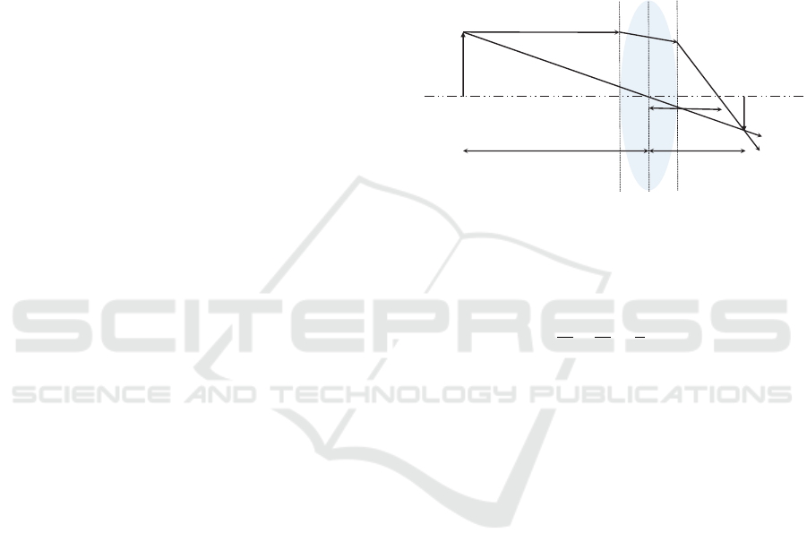
Figure 1: Focus image.
The imaging formula, also known as the lens-
maker’s formula, is as follows (Nayar and Nakagawa,
1994):
1
𝑆
+
1
𝑆
=
1
𝑓
(1)
where 𝑆
is the object distance, which is the distance
between the object and the lens; 𝑆
is the image
distance, which is the distance between the image and
the lens; and f is the focal length of the lens. It can be
seen from the lens-maker’s that a relative image
distance can be obtained from one object distance,
and vice versa. When the sample is in the object plane,
the outline of the sample is focused by the lens and
forms a sharp image. The image at this time is called
a focus image. When the sample is not in the object
plane, a circle is formed in the image plane according
to the trigonometric principle. The blurred image was
out of focus at the time.
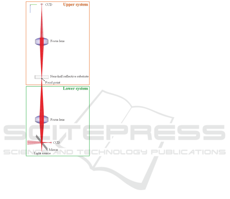
The optical design is shown in Figure 2. The
design concept is the upper and lower double light
path. The upper system includes a CCD for capturing
images, a focusing microscope objective, and a near-
half reflecting substrate. The lower system consists of
a light source, a mirror, a CCD and a focusing
microscope objective. This model is created by using
a single lens to represent the focusing microscope
objective lens, and it is selected as a standard product.
The purpose is to establish the model in the simplest
way. If a good focusing effect can be achieved with
this structure, a more accurate result can be obtained
Object
Image
Lens
f
𝑆
𝑆
A Study on Double-sided Optical Focusing Alignment of Transparent Substrate
81
by replacing the focusing microscope objective during
actual measurement. Since only surface reflection is
considered, the focus position is designed on the lower
surface of the near-half reflecting substrate.
Figure 2: Schematic diagram.
The Figure 2 shows, the light source transmits
through the half mirror to the focus lens, focusing on
the lower surface of the near semi-reflective substrate,
which is the focus position. Due to the dual optical path
design, the light will have two paths. A part of the light
is reflected by the lower surface and returned to the
CCD of the lower system. The other part of the light
continues to propagate through the near-half reflecting
substrate. After passing through the focusing lens,
focus on the CCD of the upper system.
The wavelength of the simulated light source is 550
nm representing the visible light band. The mirror is
50% transmitted and 50% reflective. The lens has a
curvature of 10 mm, the thickness is 5 mm, the material
is BK7, and no surface coating. The near-half
reflecting substrate has a length of 10 mm and a width
of 10 Mm, thickness 2 mm, material BK7. In this paper,
non-sequential optical tracking does not consider
optical wave effects. Because the diffraction and near-
field effects caused by the objects in the experimental
structure are negligible. In the process of optical
simulation, the material and interface have been
correctly set, so the calculation of Fresnel equations
will be considered and calculated by the FRED optical
simulation software.
3 EXPERIMENTAL RESULTS
AND DISCUSSION
In order to obtain a clear image when the CCD of the
upper and lower systems is in the focus position, the
upper surface and the lower surface of the near-half-
reflective substrate are coated, which is determined by
simulation. The clarity of the image is positively
correlated with the optical energy density, so the
energy density can be used as a basis for judging the
clarity of the image.
The simulation results are shown in Figure 3. First,
the reflection and transmittance of pure glass materials
are analysed. At the focus position, the energy density
received by the upper system is much larger than that
received by the lower system, which is about 33.5
times. In other words, in the case where the upper and
lower surfaces of the near-half-reflective substrate are
not coated, only the upper system can capture a clear
image, and the lower system can only receive a very
weak and blurred image. In order to improve the
excessive difference in energy density between the
upper and lower systems, the reflective coatings on the
lower surface of the near-half-reflective substrate were
simulated at 30%, 60%, and 80%, respectively. Among
them, in the case of 30% and 80% reflective coating on
the lower surface coating, the difference in energy
density between the upper and lower systems is 3.46
and 0.37 times, respectively. Only one of the systems
can receive clear images at the focus position, not both
systems simultaneously. For both systems to capture a
clear image, the lower surface needs to be plated with
a 60% reflective coating to receive a clear image at the
same time, as shown in Figure 3. This coating
specification is ideally feasible, but in fact, the coating
quality and mechanism error must also be considered,
so it needs to be measured to determine.
In order to calibrate the assembly error of the
system and components, the CCD and lens of the
above system are used as the reference to simulate the
four assembly conditions, which are the lower system
is displaced in the Z-axis direction, shifted in the Y-
axis direction, the angle θ is tilted with the light source
as a centre, and the near-half-reflective substrate is
tilted at an angle ψ from the centre of the substrate, as
shown in Figure 4.
PHOTOPTICS 2020 - 8th International Conference on Photonics, Optics and Laser Technology
82
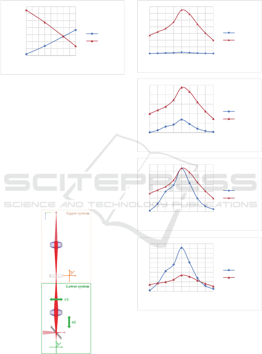
Figure 3: Energy density change plots for different coating
systems.
In the case of different reflective coatings, the
lower system is offset in the Z-axis direction, and the
Z-direction offset can be adjusted by the difference in
energy density between the upper and lower systems,
and the range is ±1 mm, as shown in Fig. 5 (a). (b),
(c) and (d). However, in the case of uncoated, it is
difficult to adjust compared to other cases where there
is a coating. Wherein, as observed in Figure 5, the left
and right curves are asymmetrical because the focus
position will be in the near semi-reflective substrate
when the lower system is closer to the upper system;
when the lower system is far away from the upper
system, the focus position will be in the air, and due
to the refractive index of the substrate and air are not
the same, so the energy density near and away from
the system is asymmetric.
Figure 4: System and component assembly error types.
(a)
(b)
(c)
(d)
Figure 5: Substrate (a) uncoated, (b) 30%, (c) 60%, and (d)
80% reflective coating, lower system energy density
variation.
Since the energy density of the upper and lower
systems can be made the same when the lower surface
of the substrate is 60% reflective coating, it is used as
0,00
50,00
100,00
150,00
200,00
250,00
300,00
350,00
0 1020304050607080
Energy Density (W/mm2)
Lower surface AR coating (%)
Lower system
Upper system
0,00
50,00
100,00
150,00
200,00
250,00
300,00
350,00
-1 -0,75 -0,5 -0,25 0 0,25 0,5 0,75 1
Energy Density (W/mm2)
Relative position of the lower system and the substrate (mm)
Lower system
Upper system
0,00
50,00
100,00
150,00
200,00
250,00
-1 -0,75 -0,5 -0,25 0 0,25 0,5 0,75 1
Energy Density (W/mm2)
Relative position of the lower system and the substrate (mm)
Lower system
Upper system
0,00
20,00
40,00
60,00
80,00
100,00
120,00
140,00
-1 -0,75 -0,5 -0,25 0 0,25 0,5 0,75 1
Energy Density (W/mm2)
Relative position of the lower system and the substrate (mm)
Lower system
Upper system
0,00
20,00
40,00
60,00
80,00
100,00
120,00
140,00
160,00
180,00
200,00
-1 -0,75 -0,5 -0,25 0 0,25 0,5 0,75 1
Energy Density (W/mm2)
Relative position of the lower system and the substrate (mm)
Lower system
Upper system
A Study on Double-sided Optical Focusing Alignment of Transparent Substrate
83
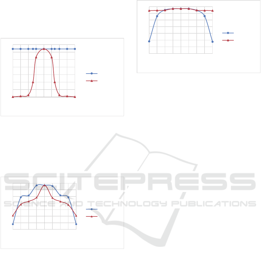
a standard sheet. When the system is offset in the Y
direction, the Y-direction offset of the lower system
can be adjusted by the maximum energy density of
the upper system, and the range is ±0.1 mm, as shown
in Figure 6.
Figure 6: System energy density change diagram under the
Y-axis offset of the lower system.
When the lower system tilts the θ angle with the
light source as the centre, the tilt of the lower system
can be adjusted by the difference in energy density
between the upper and lower systems, and the range
is ±1 ̊, as shown in Figure 7.
Figure 7: System energy density change diagram at lower
system tilt.
When the near-half-reflective substrate is tilted at
an angle ψ from the centre of the substrate, the tilt
angle can be determined by the change of the energy
density of the lower system, and the range is ±1 ̊, and
the substrate uniformity can be detected, as shown in
Figure 8.
Figure 8: System energy density change diagram of
substrate tilt.
Based on the above simulation results, in an actual
setup, a power meter and profiler is used to measure
the energy density difference between the upper and
lower systems. If the energy density of the lower
system is greater than the upper system, the tilt angle
of the substrate must be adjusted. If the energy
density difference is greater than 90, the Y-axis
displacement of the lower system must be adjusted; if
the energy density difference is greater than 20, the
Z-axis displacement of the lower system must be
adjusted first; if the energy density difference is less
than 20, the tilt of the lower system must be adjusted
angle.
4 CONCLUSIONS
The substrate coating simulation results show that the
60% coated substrate is used as the calibration
standard film, so that the upper and lower systems can
capture clear images. In the assembly error simulation
results, the Z-axis offset range of the lower system
can be effectively adjusted by ±1 mm, the lower
system tilts range ±1 ̊, and the substrate tilts range ±1
by the difference of the upper and lower energy
densities. The Y-axis offset range is ±0.1 mm by the
maximum energy density of the upper system.
Further, the uniformity of the substrate can be
detected as a result of the tilt of the substrate.
The focus positioning technology proposed in this
study is a self-developed non-contact optical
measurement module that overcomes the problems of
the traditional autofocus measurement module and
can be widely used in autofocus. It is suitable for
single point height, uniform measurement and system
assembly error detection of microstructure.
0,00
20,00
40,00
60,00
80,00
100,00
120,00
140,00
-0,1 -0,075-0,05-0,025 0 0,025 0,05 0,075 0,1
Energy Density (W/mm2)
Y-axis offset position of the lower system (mm)
Lower system
Upper system
0,00
20,00
40,00
60,00
80,00
100,00
120,00
140,00
-1 -0,75 -0,5 -0,25 0 0,25 0,5 0,75 1
Energy Density (W/mm2)
Tilt angle of the lower system (∘)
Lower system
Upper system
0,00
20,00
40,00
60,00
80,00
100,00
120,00
140,00
-1 -0,75 -0,5 -0,25 0 0,25 0,5 0,75 1
Energy Density (W/mm2)
Tilt angle of the substrate (∘)
Lower system
Upper system
PHOTOPTICS 2020 - 8th International Conference on Photonics, Optics and Laser Technology
84

ACKNOWLEDGEMENTS
The authors would like to express their appreciation for
financial aid from the Ministry of Science and
Technology, R.O.C under grant numbers MOST 108-
2221-E-492-019, MOST 108-2218-E-492-010 and
MOST 108-2622-E-492-009-CC3. The authors would
also like to express their gratitude to the Taiwan
Instrument Research Institute of National Applied
Research Laboratories for the support.
REFERENCES
Wang, X., Zheng, Z., Fan, Y., Lai, M., Wei, J., Wu, X., “A
focus automatic positioning system of high-power laser
beam based on plasma ultraviolet radiation,” High
Power Laser and Partical Beams, Vol. 31, 2019.
Chon, S. M., Choi, S. B., Kim, Y. W., Kim, K. W., Lim, K.
H., Choi, S. Y., and Jun, C. S., 2001. “Development of
automated contact inspection system using in-line CD
SEM,” IEEE, 399-401.
Zureik, E., Lyon, D., Abu-Laban, Y., Surveillance and
Control in Israel/Palestine: Population, Territory and
Power, Routledge, 2010.
Browne, M. A., Akinyemi, O., and Boyde, A., 1992.
“Confocal surface profiling using chromatic
aberration,” Scanning, Vol. 14, 145-153.
Maly, M. and Boyde, A., 1994. “Real-time stereoscopic
confocal reflection microscopy using objective lens
with linear longitudinal chromatic dispersion,”
Scanning, Vol. 16, 187-192.
Tiziani, H. J., and Uhde, H. M., 1994. “3-Dimensional
image sensing by chromatic confocal microscopy,”
Appl. Opt., Vol. 33, 1838–1843.
Kim, T., Kim, S. H., Do, D., Yoo, H., and Gweon, D., 2013.
“Chromatic confocal microscopy with a novel
wavelength detection method using transmittance,”
OPTICS EXPRESS, Vol. 21, 6286-6294.
Nayar, S.K., and Nakagawa, Y., “Shape from focus
system,” 1994. IEEE, Vol. 16, 824-831.
A Study on Double-sided Optical Focusing Alignment of Transparent Substrate
85
