
Characterization on Surface Morphology of GaN Layer
Deposited on 2D MoS
2
Developed by CVD System
Iwan Susanto
1,2
, Ing-Song Yu
1
, Chi-Yu Tsai
1
, Yen-Ten Ho
3
, Ping-Yu Tsai
4
, Dianta Mustofa Kamal
2
,
Belyamin
2
, Sulaksana Permana
5
1
Department of Materials Science and Engineering, National Dong Hwa University, Hualien 97401, Taiwan ROC
2
Department of Mechanical Engineering, Politeknik Negeri Jakarta, Depok 16424, Indonesia
3
International College of Semiconductor Technology, National Chiao Tung University, Hsinchu 300, Taiwan ROC
4
Department of Electronic Systems Research Division, Chung-Shan Institute of Science & Technology,
Tao-Yan 325, Taiwan ROC
5
Center of Mineral Processing and Corrosion Research, Department of Metallurgy and Materials Engineering,
Universitas Indonesia, Depok 16424, Indonesia
Keywords: Characterization, Gallium Nitride, Molybdenum Disulfide, Chemical Vapor Deposition, Molecular Beam
Epitaxy
Abstract: A few layers of GaN was deposited epitaxial on the MoS
2
layers by PA-MBE technique. A smooth surface
with mixed like-flakes of MoS
2
is provided by the development of CVD system. It is grown on the c-sapphire
substrate with a few layers. Further, surface morphology both of MoS
2
substrate and GaN layer was
investigated in detail by the AFM and FE-SEM characterization. The results demonstrated that the surface
morphology of the constructing GaN layer was smoother than MoS
2
layer. The surface texture was obtained
throughout the decreasing of area roughness up to 1.44 nm and root mean square (RMS) of 2.40 nm. However,
thin GaN layers covering the MoS
2
surface was in the less content of atomic with a weight Ga element. It
takes longer growth time and more flux to obtain a flat morphological surface with high smoothness.
1 INTRODUCTION
GaN included on the group III-IV semiconductor
materials has excellent properties such as high
conductivity, high electrons mobility, very hard
material, chemically and mechanically stable
(Kawashima et al., 1997; Hanada, 2009). In
accordance with those properties, GaN is used
extensively for application in optoelectronic,
electronic components, high-power and high-
frequency devices (Chen et al., 2017; Su, Chen and
Rajan, 2013; Würtele et al., 2011; Joshin et al., 2014).
However, since a high-cost of the GaN bulk (Liu and
Edgar, 2002), GaN layers are developed to be grown
on other materials substrate. Several materials are
attempted for providing GaN layers as a substrate
(Kukushkin et al., 2008). Unfortunately, distinguish
thermal expansion coefficient and the lattice-
mismatched might build the residual strain initiated
the defect as decreasing the temperature from
manufacturing (Trampert, 2002; Poust et al., 2003).
The beginning of the damage raised from the
interface and then spread it toward the surface of layer
(Trampert, 2002; Fachruddin et al., 2020), which
degrade the quality structure and reduction for long-
term application.
Recently, several studies have been devoted for
increasing the GaN quality by growing it near lattice
matched (Susanto et al., 2019; Gupta et al., 2016; and
Mánuel et al., 2010). 2D MoS
2
layers was a hot topic
when they were grown on GaN material as
semiconductor material for optoelectronic application
(Wan et al., 2018; Zhang et al., 2018). Moreover,
MoS
2
has a lattice-matched with GaN which promises
for the high-quality growing of GaN layers. As thick
layers of GaN films were grown up to it's thick of 1.8
µm (Kimura et al., 2005), the defects are not attended
on the film's surface. Besides, an investigation of the
surface morphology of the GaN layer near the
substrate has not been studied in detail. It could be an
exciting part to observe it.
In this report, the morphology of GaN films will
be characterized to get a deep understanding of the
contour and texture of surface condition. A few
Susanto, I., Yu, I., Tsai, C., Ho, Y., Tsai, P., Kamal, D., Belyamin, . and Permana, S.
Characterization on Surface Morphology of GaN Layer Deposited on 2D MoS2 Developed by CVD System.
DOI: 10.5220/0010537900003153
In Proceedings of the 9th Annual Southeast Asian International Seminar (ASAIS 2020), pages 93-96
ISBN: 978-989-758-518-0
Copyright
c
2022 by SCITEPRESS – Science and Technology Publications, Lda. All rights reserved
93
epitaxial growth parameters will be used to deposit
the impinging Ga and N atom on the 2D MoS
2
layer.
The characterization results will be presented and
analyzed based on both of 2-dimensional (2D) images
and quantitative data observation of AFM and SEM
technique.
2 EXPERIMENTAL METHOD
The growing GaN films on 2D MoS
2
layers are
prepared by MBE technique. The growth GaN was
controlled at 600 ℃ for 20 minutes. The thermal
cleaning is given for 40 minutes and free-nitridation
of 10 minutes before the epitaxial growth. The
imaging atom of Ga flux is provided by K-cell at 800
℃, while Radiofrequency of Nitrogen Gun supplied
N flux at 500 W. The flow rate was provided in sccm
of 0.8 for N6 gas. Furthermore, the background
pressure was built at 8 x 10⁻⁶ Torr. The 2D MoS
2
layer substrate was exploited by the CVD method,
deposited on the single crystal of c-sapphire. Finally,
the ex-situ characterization was employed using
AFM and FE-SEM machine for investigating the
surface morphology.
3 RESULT AND DISCUSSION
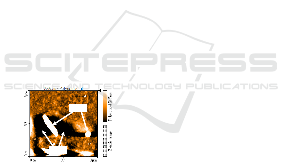
Figure 1. AFM image of 2D MoS
2
layer deposited on the
sapphire substrate
Fig 1 displays the surface morphology of MoS
2
layer
grown on the sapphire. The surface texture 2D MoS
2
layer was observed with 3 x 3 µm of scan area. The
bright color was related to peak of MoS
2
on the
surface, while the dark color was associate with the
valley of the surface. The difference both of the colors
elucidate the surface condition formed on the MoS
2
layer. The MoS
2
like-steps with the bright color, and
the dark area formed was associated with the surface
contour of the MoS
2
layer during the deposition
process using the CVD system. The area roughness of
MoS
2
surface is achieved to be 2.17 nm and the root
mean square is obtained about 4.19 nm. The high
peak value and the deep valley are 25.14 nm, and
31.99 nm, serially. Based on the characterization
using the AFM method, the texture of the MoS
2
layer
is established with smoother of surface condition.
Since the growth epitaxial, the morphology of
GaN layers on 2D MoS
2
has entirely demonstrated in
Fig 2. The surface texture GaN layer was observed
with a scan area of 3x3 µm in Fig 2(a). The bright
color was related to peak of GaN on the surface, while
the dark color was associate with the valley of the
surface in Fig 2(b). The surface texture was more
apparent as they were demonstrated using the 3-
dimension profile shown in Fig 2(c). The distinct
colors seem with a low degradation value, suggesting
the smooth surface formed on the GaN layer.
However, attending the protrusions, GaN like-steps
on the surface in Fig 2(a) could be increasing the
surface roughness on GaN layer. The GaN like-steps
formed was initiated with the surface contour of the
MoS
2
layer exhibited on Fig 1. As the impinging Ga
and N atoms on the MoS
2
layer, the GaN layer grew
epitaxial following the substrate's texture. So, in the
short growth time, the GaN layer formed based on the
substrate surface pattern (Susanto et al., 2019).
Furthermore, the area roughness on the surface GaN
has reached up to 1.44 nm and the root mean square
is 2.40 nm. The highest peak value is up to 21.07 nm
and the deep valley is until 15.01 nm. According to
the AFM images, the surface GaN layer constructed
with smoother than the MoS
2
surface. The smoother
of surface morphology as indicated by decreasing the
area roughness and root mean square up to 33.6 % and
44.7 %, respectively.
Fig 3 exhibit the FE-SEM images and EDS
observation of the surface morphology and element
composition on the GaN layer. By the magnitude of
15,000 displayed in Fig 3(a), the surface GaN layer's
condition looks smooth, indicating that it has grown
on the MoS
2
layer. However, the GaN like-flakes
were still visible on the surface, which is in tune to
the AFM images in Fig 2. Observation using the spot
scans in spectrum one on Fig 3(b) was carried out to
identify the GaN layer. Fig 3 show Ga element
detected in spectrum 1 with less content, suggesting
that the few GaN layers have grown on the MoS
2
flakes. All elements related to substrate layers were
tabulated more detail in Table 1. GaN layers have
successfully covered all of surface MoS
2
layer even
in the less content of percentage atomic with a
percentage weight Ga element.
Valley
Peaks
ASAIS 2020 - Annual Southeast Asian International Seminar
94
Figure 2. AFM images of surface GaN layer observed; (a) Scan area profile of 3x3 µm, (b) line-profile through of 3 µm, and
(c) 3-dimension profile with a deep of 20 nm
Figure 3. SEM images of surface morphology GaN layers (a, b), and (c) EDS of scan-spot on the surface GaN like-flakes
4 CONCLUSIONS
The characterization of surface morphology on the
GaN layer deposited on 2D MoS
2
layer by PA-MBE
system was successfully done using AFM and FE-
SEM technique. The surface texture of MoS
2
layers
was observed in detail for initial surface condition of
the substrate. Besides part for MoS
2
plat-layers,
attending MoS
2
like-flakes leads to establishing the
texture of GaN layers epitaxial. A less content of
atomic and weight Ga also covered the surface of
MoS
2
plat-layers. Even though the epitaxial was
employed in the short growth time, the decreasing of
the area roughness and root mean square attained the
smoother surface of the GaN layer. Thicker GaN
films should be employed by providing a higher Ga
and N fluxes with longer growth time.
Characterization on Surface Morphology of GaN Layer Deposited on 2D MoS2 Developed by CVD System
95

ACKNOWLEDGMENTS
The authors would like to thank Ministry of Science
and Technology, Taiwan for financially supporting
this study (MOST 107-2221-E-259- 001-MY2 and
107-3017-F-009-002), and a giving thanks to Pusat
Penelitian dan Pengabdian Masyarakat, Politeknik
Negeri Jakarta (PPPM PNJ nomor B.142 /PL3.18
/PN.00.03 /2020) and also for the Ministry of
Research and Technology, Research Council, and the
National Innovation Republic of Indonesia
REFERENCES
Chen, K. J. et al. (2017) ‘GaN-on-Si power technology:
Devices and applications’, IEEE Transactions on
Electron Devices. doi: 10.1109/TED.2017.2657579.
Fachruddin, et al. (2020) ‘Surface Modification of
Magnetic TiO
2
Core-Shell with Doped Cerium for
Enhancement of Photocatalytic Performance’, Eastern-
European Journal of Enterprise Technologies. doi:
10.15587/1729-4061.2020.203186
Gupta, P. et al. (2016) ‘Layered transition metal
dichalcogenides: promising near-lattice-matched
substrates for GaN growth’, Scientific Reports. doi:
10.1038/srep23708.
Hanada, T. (2009) ‘Basic Properties of ZnO, GaN, and
Related Materials’, in. doi: 10.1007/978-3-540-88847-
5_1.
Joshin, K. et al. (2014) ‘Outlook for GaN HEMT
technology’, Fujitsu Scientific and Technical Journal.
Kawashima, T. et al. (1997) ‘Optical properties of
hexagonal GaN’, Journal of Applied Physics. doi:
10.1063/1.365671.
Kimura, R. et al. (2005) ‘Thick cubic GaN film growth
using ultra-thin low-temperature buffer layer by RF-
MBE’, Journal of Crystal Growth, 278(1–4), pp. 411–
414. doi: 10.1016/j.jcrysgro.2005.01.058.
Kukushkin, S. A. et al. (2008) ‘Substrates for epitaxy of
gallium nitride: New materials and techniques’,
Reviews on Advanced Materials Science.
Liu, L. and Edgar, J. H. (2002) ‘Substrates for gallium
nitride epitaxy’, 37, pp. 61–127.
Mánuel, J. M. et al. (2010) ‘Structural and compositional
homogeneity of InAlN epitaxial layers nearly lattice-
matched to GaN’, Acta Materialia. doi:
10.1016/j.actamat.2010.04.001.
Poust, B. D. et al. (2003) ‘SiC substrate defects and III-N
heteroepitaxy’, Journal of Physics D: Applied Physics.
doi: 10.1088/0022-3727/36/10A/321.
Su, M., Chen, C. and Rajan, S. (2013) ‘Prospects for the
application of GaN power devices in hybrid electric
vehicle drive systems’, Semiconductor Science and
Technology. doi: 10.1088/0268-1242/28/7/074012.
Susanto, I., Tsai, C., et al. (2019) ‘Morphology and surface
stability of GaN thin film grown on the short growth
time by Plasma Assisted Molecular Beam Epitaxy’, J.
Phs : Conference Seriese, 1364(012067). doi:
10.1088/1742-6596/1364/1/012067.
Susanto, I., Tsai, C.-Y., et al. (2019) ‘The influence of 2D
MoS
2
layers on the growth of GaN films by plasma-
assisted molecular beam epitaxy’, Applied Surface
Science, 496(July), p. 143616. doi:
10.1016/j.apsusc.2019.143616.
Trampert, A. (2002) ‘Heteroepitaxy of dissimilar materials:
Effect of interface structure on strain and defect
formation’, in Physica E: Low-Dimensional Systems
and Nanostructures. doi: 10.1016/S1386-
9477(02)00317-X.
Wan, Y. et al. (2018) ‘Epitaxial Single-Layer MoS
2
on GaN
with Enhanced Valley Helicity’, Advanced Materials.
doi: 10.1002/adma.201703888.
Würtele, M. A. et al. (2011) ‘Application of GaN-based
ultraviolet-C light emitting diodes - UV LEDs - for
water disinfection’, Water Research. doi:
10.1016/j.watres.2010.11.015.
Zhang, Z. et al. (2018) ‘Interface Engineering of Monolayer
MoS
2
/GaN Hybrid Heterostructure: Modified Band
Alignment for Photocatalytic Water Splitting
Application by Nitridation Treatment’, ACS Applied
Materials and Interfaces. doi: 10.1021/acsami.8b01286.
ASAIS 2020 - Annual Southeast Asian International Seminar
96
