
Micro Topography on Tool Steel Processed using Wire Electrical
Discharge Machining
Rifky Maulana Yusron
1
, Dhika Aditya Purnomo
2
Saiful Arif
3
and Rahayu Mekar Bisono
3
1
Department of Mechanical Engineering, University of Trunojoyo Madura,, Bangkalan, Indonesia
2
Department of Design and Manufacture Engineering, Shipbuilding Institute of Polytechnic Surabaya, Surabaya, Indonesia
3
Dept. Mechanical Engineering, Polytechnic State of Malang, Malang, Indonesia
Keywords: Measurement, micro surface topography, open voltage, pulse on-time, surface roughness, Wire-EDM.
Abstract: Wire Electrical Discharge Machining (Wire-EDM) using electrical energy to cutting materials, they penetrate
material not continuously instead penetrate with a specific interval that called as a pulse on time. Open voltage
is a variable to control value of penetrate energy. Material removal rate caused melted and evaporation work
piece material. Flushing by dielectric fluid affected quenching on the surface machined materials. During
Wire-EDM process, re-heating of melted material. Constant quenching and re-heating also caused the craters
to be relatively deep and width on a microscale. That’s craters affected has impact on surface roughness on
macro scale. In Wire-EDM process, surface roughness is important to describe deviation characteristic on
surface of workpiece. A research conducting to observe micro topography by using variable pulse on time
and open voltage, including surface roughness on tool steel surface who has processed using Wire-EDM. This
research using design experiment factorial 3x3. Surface roughness measurement conducting using Mitutoyo
surftest. Surface electron measurement (SEM) used to observe micro topography on workpiece surface. From
this research we can conclude that pulse on-time and open voltage directly proportional to surface roughness
response variable. From this research was achieve lowest surface roughness 1,33 μm on combination pulse
on time 2 µs and open voltage 75V and the highest surface roughness 2,52 μm on combination pulse on time
6 µs and open voltage 105V.
1 INTRODUCTION
Although equipped with advanced technology
conventional machining processes, still insufficient to
process high hardness material and complex contours
which cannot be complete with conventional
machining processes. To solve the problem, the
machining industry is now wide applied non-
conventional machining processes. Wire-EDM
process is one of nonconventional machining who use
electrical energy to produce sparks between anode
and cathode, then convert spark into thermal energy
with temperature about 8.000
o
C to 20.000
o
C
(Kutuzova & Melnik, 2018). Current penetrate from
electrode to workpiece with frequency about 20.000
Hz to melting 30.000 Hz, it made both melting and
evaporating (Jaiswal, Peshwani, Shivakoti, &
Bhattacharya, 2018). During Wire-EDM process,
cutting process not conducted continuously. It come
since pulse on-time phase and stop when it entering
pulse off-time phase (Liu et al., 2017). During Wire-
EDM process, the cutting process not conducted
continuously. It come since pulse on-time phase and
stop when it pulse off-time phase. It might to avoid
wire rupture caused stress during machining process
(Calvo, Daniel, Calvo, & Daniel, 2020).
Wire-EDM applied on industrial since 1950
(Bravo et al., 2018) and has continuous development
technology, the current research has asynchronous
control mode to meet Industrial 4.0 requirement
(Zhou, Jing, Yang, Yao, & He, 2018). It has an ability
to processing mechanical part who require complex
shape, high precision and low surface roughness
(Zhou, Wu, Xu, Mu, & Dou, 2018). There is wide
application of Wire-EDM including aerospace,
nuclear, automotive, tools, jewellery, mould, dies,
and also medical equipment industries (Wälder et al.,
2018). Wire-EDM have a capability to process hard
materials more effective than conventional
machining process, those materials such as titanium,
nimonic alloy, and zirconium. But, Wire-EDM
machining process has their own problems such as
Yusron, R., Purnomo, D., Arif, S. and Bisono, R.
Micro Topography on Tool Steel Processed using Wire Electrical Discharge Machining.
DOI: 10.5220/0010305600003051
In Proceedings of the International Conference on Culture Heritage, Education, Sustainable Tourism, and Innovation Technologies (CESIT 2020), pages 165-172
ISBN: 978-989-758-501-2
Copyright
c
2022 by SCITEPRESS – Science and Technology Publications, Lda. All rights reserved
165
forming of micro heat affective zone (HAZ), recast
layer, micro-crack, porosity, local hardening or
annealing, grain growth and forming of alloy
incidentally because element transfers phenomena
from wire or dielectric, its might new alloy formed on
recast layer (Soundhar, Zubar, Thariq, Haji, &
Sultan, 2019).
On this research Buderus 2080 tool steel applied
as material specimen. This material has high
resistance against wear, stability on heat treatment. It
wide applied on industrial manufacture, it is common
being material to make deep drawing dice, shearing
blade, broaching tool, sand blasting nozzle, trimming
dies and plastic mould. Buderus 2080 tool steel has
chemical composition Carbon about 1.90-2.00%.
Silicon about 0.20-0.30%. Manganese about 0.25-
0.30% Chromium about 9.80-12.00%. Based on
carbon composition, this material classified as high
carbon steel. High carbon steel is strong but brittle, to
improve mechanical properties by applied heat
treatment such as austenizing, quenching, and
tempering (Jatti, 2018). Tempering can transform
their grain be martensite, then make material not just
hard but also ductile. This process cover the original
material disadvantage (Kou & Han, 2018).
The aim from this research is to observe influence
from parameters pulse on-time and open voltage to
surface roughness and micro topography on Buderus
2080 tool steel using Wire-EDM.
2 METHODS
On this research Wire-EDM using CHMER CW
32GF. Movement direction followed by five axis (x,
y, z, u, and v) Wire diameter holder 0,15–0,30 mm.
Maximum wire cutting 250 mm/second. Table
dimension 600 mm x 400 mm. Before cutting process
using wire EDM, each specimen had heat treatment
to reduce stress and increase hardness. Specimen has
dimension length 200 mm, width 30 mm and depth
15 mm. Specimen cutting began from left side for 10
mm with distance of each specimen about 5 mm.
After all cutting process complete and cutting length
for each experiment has measured, cut material 5mm
perpendicular from first cutting edge.
Aquadestilata applied as dielectric during machining
process. Parameter based on recommendation from
manual book of material. This research runs based on
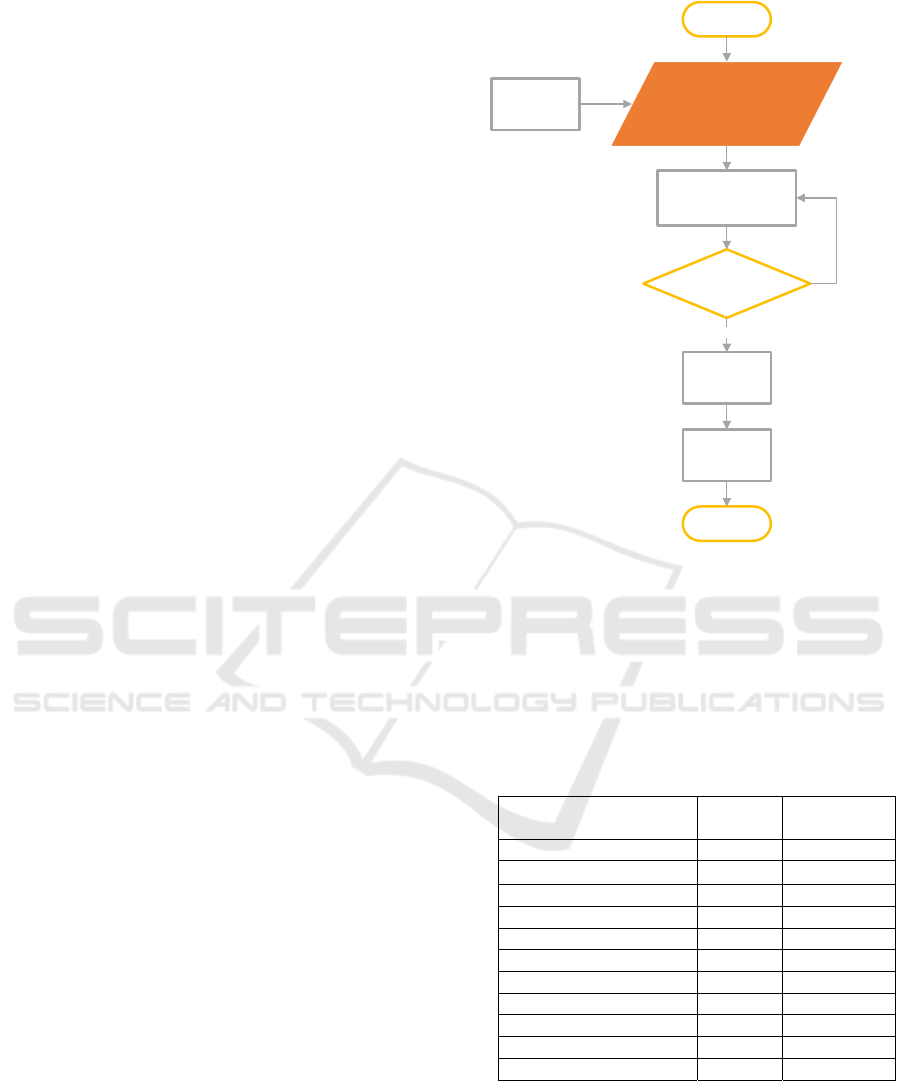
flowchart that shown on Figure 1.
START
Parameter:
pulse on-time 2, 4
and 6 µs
open voltage 75,
85 and 105 V
replicationhas
significantdifferent?
Observinguse
SEM
Yes
Literature
Review
Cuttingmaterial
Buderus2080use Zinc
coatedwire
No
Analyze
END
Figure 1: Research flowchart.
2.1 Material
This research using Buderus 2080 tool steel had heat
treatment before. The Heat treatment process shown
on Table 1. During heat treatment specimen hardness
increased from 55 HRC to 60 HRC.
Table 1: Specimen Heat Treatment Process.
Process Temp
(
o
C)
Time
(minute)
Soft Annealing
Stress Revealing
Preheating 600 45
Preheatin
g
II 850 45
Austenizin
g
960 45
Quench Media -5 Su
d
d
en
Tempering I 180 120
Tempering II 180 120
Tem
p
erin
g
II 180 120
Carburizin
g
Nitro Carburizin
g
Wire electrode using AC CUT VS 900 zinc-
coated brass wire with chemical composition Cu
about 65% and Zn about 35%. Wire tension 880
N/sq.mm. Elongation 2%. Tolerance about ± 0.001
mm.
CESIT 2020 - International Conference on Culture Heritage, Education, Sustainable Tourism, and Innovation Technologies
166
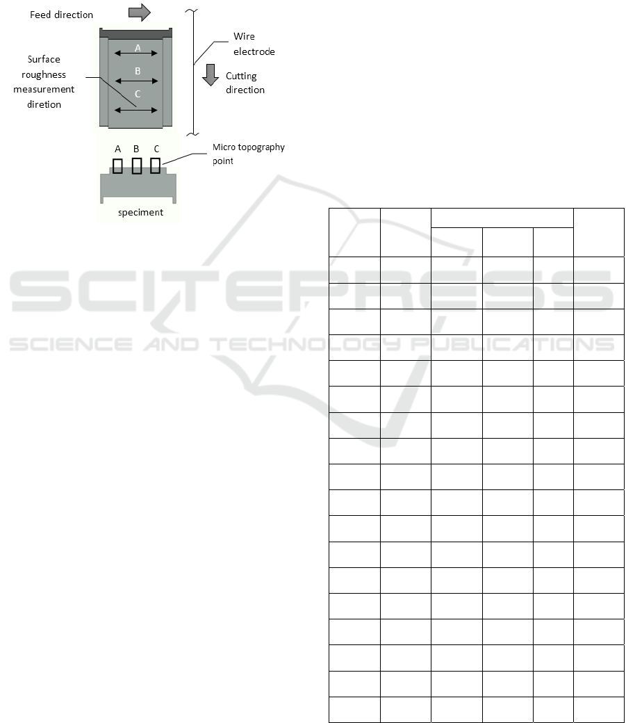
2.2 Measurement
Surface roughness measurement perpendicular to
wire cutting direction on workpiece. Mitutoyo
surftest 301 use to observe surface roughness dan
Scanning Electron Microscope (SEM) using to
observe micro topography on workpiece. Cutting
direction scheme by electrode and direction with
position of surface roughness shown on Figure 2.
Figure 2: Cutting direction scheme and surface roughness
measurement on speciment.
From Figure 2 we can see there is three point of data
collectin fron surface roughness, that collecting data
to observe is there any different surface roughness
value from each points. Image of micro surface
topography captured using 2000x zoom Scanning
Electron Microscope. Potition of micro surface
topography position shown on figure 1 below
showed with black box. This to observe is there any
different from begining, midlle and end of material
cutting.
2.3 Parameters
This research using design experiment factorial 3x3
because there is two process variable, they are pulse
on-time 3 level (2 µs, 4 µs and 6 µs) and open voltage
3 level (75 V, 85 V and 105 V). Constant variable on
this research are:
Low power (10 DCEN)
Arc off time (13 µs)
Feed rate override (9mm/s)
Wire tension (8 g)
Wire feed (10 mm/s)
Water Flow (6 kg/cm
2
)
Feed rate mode (0 servo)
Feed rate (1mm/s)
Arc on time (2 A)
Off time (12 µs)
Servo voltage (50V).
Because with this design experiment we had many
parameters using less materials. This research using
two replications for surface roughness and surface
micro topography on specimens, because we want
make sure there is no significant different in one
parameter. Surface rouhness data collecting using
Mitutoyo Surftest 301.
3 RESULT AND DISCUSSION
The implementation of research conducting with
combination variable pulse on time and open voltage
on wire EDM machining. Both process variable has
significant influence to surface roughness
Experiment result based on design experiment
factorial 3x3 shown Table 2.
Table 2: Experimental Data of Surface Roughness.
Pulse on
time
(µs)
Open
voltage
(V)
Surface roughness (µ)
Average
Point A Point B
Point
C
2 75
1,33 1,35 1,31
1,33
2 90
1,47 1,43 1,56
1,48
2 105
1,65 1,63 1,67
1,65
4 75
1,73 1,65 1,69
1,69
4 90
1,91 1,83 1,89
1,87
4 105
2,10 2,03 1,99
2,04
6 75
2,01 2,20 2,04
2,08
6 90
2,28 2,19 2,29
2,25
6 105
2,50 2,49 2,31
2,43
2 75
1,42 1,39 1,37
1,39
2 90
1,42 1,67 1,65
1,58
2 105
1,83 1,71 1,73
1,75
4 75
1,77 1,80 1,78
1,78
4 90
1,78 1,81 1,72
1,77
4 105
2,18 2,04 2,20
2,14
6 75
2,20 2,18 2,17
2,18
6 90
2,12 2,16 2,19
2,15
6 105
2,45 2,61 2,52
2,52
Micro Topography on Tool Steel Processed using Wire Electrical Discharge Machining
167
3.1 Influence Pulse on Time and Open
Voltage to Surface Roughness
Experiment result data statistically tested to
determine which process variable has a significant
effect on the response variable. Analysis of variants
(ANAVA) used to identified is there variables pulse
on-time and open voltage has affected significantly to
surface roughness response. Variable pulse on-time
and open voltage have significant inluence to surface
roughness response shown on Table 3.
Table 3: Result from Table ANAVA.
Source DF SS MS F
Pulse on
time
2 1,64431 0,82216 68,98
Open
Voltage
2 0,37788 0,18894 14,62
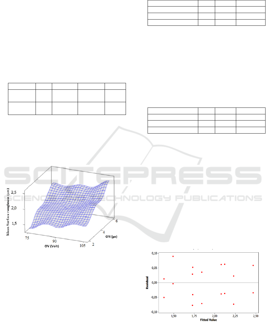
From Tabel 2 determined there is pulse on time
factor have significant influence to seuface roughness
on speciment, this value 68,98 % if comparing with
open voltage 14.62%. Surface plot for each variable
shown on Figure 2. Statistically pulse on time is a
dominant variable.
Figure 3: Surface plot ANAVA from each variable.
From surface plot on figure 2 shown incresing in
pulse on-time variable and open voltage will
increaing surface roughness value.
Beside ANAVA test we conducted Tukey Test, it
to determine level from each variable Pulse on Time
and Open Voltage who influence to surface
roughness. Table 4 show result from Tukey test on
Pulse on Time variable.
Table 4: Result from Table ANAVA.
Pulse on Time
(μ
s
)
N Mean Grou
p
in
g
66 2,3 A
46 1,9 B
26 1,5 C
Result of Tukey test on table 4 show different
result of surface roughness from pulse on time
parameters are different. The lowest mean value (1,5)
on pulse on time 2 μs and highest mean value (2,3) on
pulse on time 6 μs. Statically increasing on pulse on
time will affected on surface roughness. Based on this
test we can conclude pulse on time variable is directly
proportional to surface roughness. Tabel 5 show
result from Tukey test on Open Voltage Variable.
Table 4: Result from Table ANAVA.
O
p
en Volta
g
e
(
V
)
N Mean Grou
p
in
g
105 6 2,1 A
90 6 1,9 B
75 6 1,7 C
Like Table 4 result of Tukey test on table 5 show
different result of surface roughness from Open
Voltage parameters are different. The lowest mean
value (1,5) on Open Voltage 75V and highest mean
value (2,1) on Open Voltage 105 V. Statically
increasing open voltage will affected on surface
roughness. Based on this test we can conclude pulse
on time variable is directly proportional to surface
roughness, but Pulse on Time has more significant
volume than Open Voltage. It shows that result of
surface roughness is different at the three different
Open Voltage levels. Analysis of variance requires
that the residuals must meet three assumptions;
identical, independent and normality distributed with
zero mean with a certain variance.
Result of identical test show on figure 4
Figure 4: identical test diagram.
Figure 4 shows that the residuals (marked with re
dots) are randomly distributed around the zero line
and not form a specific pattern. Thus the identical
CESIT 2020 - International Conference on Culture Heritage, Education, Sustainable Tourism, and Innovation Technologies
168
residual assumption is fulfilled. this shows that all
data are different
Independent test on this research conducted using
auto correlation function (ACF). Based on ACF show
on figure 5, there is nothing ACF value lag out from
interval. This proves that there is no correlation
between residuals, meaning that the residuals are
independent.
Figure 5: Plot ACF on surface roughness respons.
Residual normality test residual conducted using
Kolmogorov-Smirnov test. Hipotesis that applied are:
H
0
: Residuals are normally distributed
H
1
: Residuals are not normally distributed
H
0
rejected if p-value less than α = 0,05. Result of
normality test show on Figure 6.
Figure 6: Plot of normality distribution test on surface
rouhness response.
From Kolmogorov-Smirnov test conclude:
p-value 0,116 it mean bigger than α = 0,05.
Therefore, it can be concluded that H
0
failed to
be rejected or that residuals were normally
distributed.
Mean value about -4,9343x10⁻¹⁷ it mean very
small and close to zero.
Variance on residual is about (0,182)2 =
0,03312
Thus the assumption of a normally distributed
residual with a mean value equal to zero (or close to
zero) and having a certain variation (amounting to
0.03312) has been fulfilled. Graphically, the
relationship between the Pulse on Time and Open
Voltage factors in the Wire EDM machining process
to the surface roughness response is shown in Figure
7.
Figure 7: Plot graphic influence factor Pulse on Time and
Open Voltage to surface roughness.
A fter passing, identical, independent and
normality test. It can be concluded that the pulse on
time and open voltage have an influence on the
surface roughness statistically. phenomena can be
explained that high pulse on-time lead to consequence
a phenomena called “double sparkling” and higher
local spark, it confirmed by another research (Nur,
Muas, & Risal, 2019) (Dabade & Karidkar, 2016).
Double sparkling come while high pulse on time, it
might produce higher frequency of spark. That spark
penetrates to work piece then followed with next
spark briefly. a higher pulse on-time make frequency
of thermal energy who transferred on work piece get
higher (Degenhardt, Stief, Dantan, Etienne, & Siadat,
2018). It leads to heat transfer from out surface of
workpiece to next layer (Klocke, Welschof, Herrig, &
Klink, 2018). That heat transfer conducted deeper,
then more work piece will erode. Work piece erode
randomly on a length cutting area, there deviates from
linear reference. If deviation got higher, it will have
affected on surface roughness value. Double
sparkling phenomena appear on pulse on time 4 µs
and 6 µs. High open voltage parameter causes a
voltage between work piece and wire electrode be
higher. Voltage bring out to a discharge. High
discharge energy, followed by increasing thermal
energy transferred to work piece. That will erode
work piece and lead to material removal. On micro
scale it brings out a crater on surface of work piece.
Increasing of thermal energy who transferred from
workpiece forming deeper crater (Özerkan, 2018)
(Marelli, Singh, Nagari, & Subbiah, 2020).
Micro Topography on Tool Steel Processed using Wire Electrical Discharge Machining
169
3.2 Micro Surfae Topography on Work
Piece
Globule is a part of molten metal, it spotted on surface
of work piece randomly. Globule formed by trap gas
and stack up on material and quenched by dielectric
during machining (Kou & Han, 2018). Pockmark
formed by erosion material during machining, then
turn out concavity profile like crater on surface of
workpiece. During machining process there current
between wire electrode and materials, it leads to
spark. That spark penetrates on workpiece, then
performed craters on workpiece. Debris is part from
workpiece and spreads eroded during machining
process. Bouncing out Material and re-attaching from
workpiece because laminar wave performed by
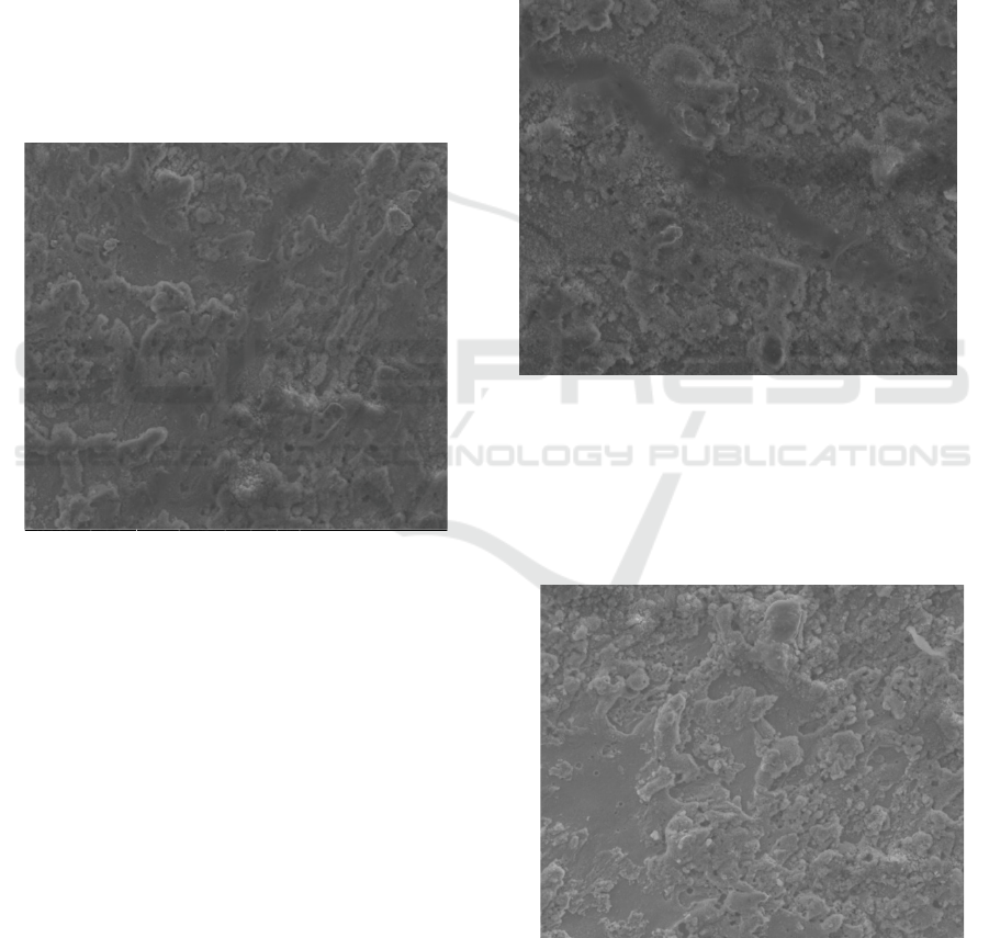
electrode flushing (Jagtap, 2018). Figure 8 to 10 is
image result processing using SEM with 2000x.
Figure 8: Micro surfaec topography on workpiece with
combination parameters 2µs and open voltage 105 V.
Figure 8 shown micro-topography performed by
pulse on-time 2 µs and open voltage 105 V, from this
combination formed rare pockmark, but have large
diameter pockmark. Current from discharge erode
work piece during machining process. Diameter size
of pockmark and current are directly proportional, it
means the highest current lead to a large diameter of
pockmark. On this combination founded a few
globules.
Figure 8 show pockmark and crater spotting rare
and with small diameter comparing from figure 4. On
this figure show surface micro-topography on
workpiece combination parameters 6µs and open
voltage 105 V. Observing on figure show surface
from work piece covered by pockmark as long as
surface of material, but with small diameter
pockmark. Many globules formed and concentrate in
specific area. There is much crater formed on material
surface on this combination. Surface of workpiece
spotting debris. Much pockmark and spread on
surface of materials phenomena, caused by high pulse
on-time on this combination. As a consequences
spark penetrate to materials with high frequency, then
more material eroded. Open voltage and discharge are
directly proportional. Low discharge makes penetrate
on material shallow, then forming low depth of
pockmark. By and large that open voltage is a
variable that influencing size of pockmark, pulse on-
time is variable influencing number of pockmarks.
Figure 9: Micro surface topography on workpiece with
combination parameters pulse on-time 2 µs and open
voltage 75 V.
Figure 9 show that pockmark covered major
surface of material and have big size comparing to
figure 8. From this image visibly large diameter crater
formed.
Figure 10: Micro surfaec topography on workpiece with
combination parameters pulse on-time 2 µs and open
voltage 75 V.
CESIT 2020 - International Conference on Culture Heritage, Education, Sustainable Tourism, and Innovation Technologies
170
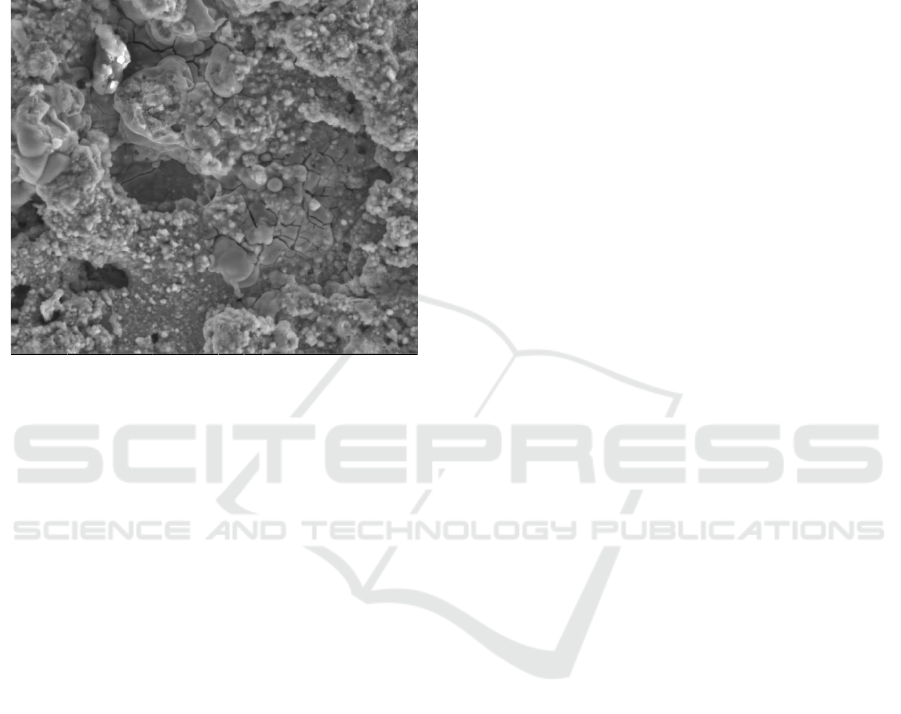
Figure 10 shown surface micro topography with
6000 x zoom from variable pulse on time 6us and
open voltage 105V, visible presence of micro-crack
on surface. It impact of double spark, it make spark
penetrate twice simultaneously, followed by flushing.
These event like quenching. From this image deep
crater visible.
Figure 11: Micro crack visible on 6000x scale.
4 CONCLUSIONS
On wire-EDM machining, variable pulse on-time set
frequency from cutting phase. Open voltage variable
set value energy consumption during cutting process.
On micro scale high pulse on-time increasing number
of pockmark and crater, high open voltage increasing
size of pockmark and crater. Number and size of
pockmark and crate influencing surface micro
topography on work piece. Profile of micro
topography influencing surface roughness of work
piece on macro scale. Surface roughness parameters
are widely used to identify surface characteristics.
Because the surface roughness value is more sensitive
detecting changes that occur in machining process.
Thus, if there are signs of increasing surface
roughness then quick taking prevention. The results
of statistical analysis of experimental data show that
surface roughness increases with increasing Pulse on
Time then Open Voltage value.
ACKNOWLEDGEMENTS
Authors wishing to acknowledge to DIPA Faculty of
Engineering University of Trunojoyo Madura 2020 to
fouding this article publication.
REFERENCES
Bravo, H., Ayesta, I., Sanchez, J. A., Zamakona, I.,
Izquierdo, B., Flaño, O., & Campo, J., 2018. Study of
interpolation strategies to dress electrodes by means of
EDM. Procedia CIRP, 68(April), 393–398.
https://doi.org/10.1016/j.procir.2017.12.101
Calvo, R., Daniel, M., Calvo, R., & Daniel, M., 2020.
ScienceDirect ScienceDirect ScienceDirect Wire
electrical discharge machining ( EDM ) setup
parameters influence in functional surface roughness
Wire electrical discharge machining ( EDM ) setup
parameters influence in functional surface roughness 8
th Ma. Procedia Manufacturing, 41, 602–609.
https://doi.org/10.1016/j.promfg.2019.09.048
Dabade, U. A., & Karidkar, S. S., 2016. Analysis of
Response Variables in WEDM of Inconel 718 Using
Taguchi Technique. Procedia CIRP, 41, 886–891.
https://doi.org/10.1016/j.procir.2016.01.026
Degenhardt, U., Stief, P., Dantan, J., Etienne, A., & Siadat,
A., 2018. ScienceDirect ScienceDirect ScienceDirect
Investigation on Wire-EDM Finishing of Titanium
Nitride Doped Investigation Wire-EDM Finishing of
Titanium Nitride Doped Silicon Nitride in CH-based
Dielectrics Silicon Nitride in CH-based Dielectrics A
new method. Procedia CIRP, 77(Hpc), 650–653.
https://doi.org/10.1016/j.procir.2018.08.185
Jagtap, S., 2018. ScienceDirect ScienceDirect
ScienceDirect Optimization of Micro EDM Drilling
Process Parameters for Optimization of Micro EDM
Drilling Process Parameters for Titanium Alloy by
Rotating Electrode Titanium Alloy by Rotating models
for capacity optimization . Procedia Manufacturing,
20, 119–126.
https://doi.org/10.1016/j.promfg.2018.02.017
Jaiswal, A., Peshwani, B., Shivakoti, I., & Bhattacharya, A.,
2018. Multi response Optimization of Wire EDM
Process Parameters. IOP Conference Series: Materials
Science and Engineering, 377(1).
https://doi.org/10.1088/1757-899X/377/1/012221
Jatti, V. S., 2018. Multi-characteristics optimization in
EDM of NiTi alloy, NiCu alloy and BeCu alloy using
Taguchi’s approach and utility concept. Alexandria
Engineering Journal, 57(4), 2807–2817.
https://doi.org/10.1016/j.aej.2017.11.004
Klocke, F., Welschof, L., Herrig, T., & Klink, A., 2018.
ScienceDirect ScienceDirect ScienceDirect Evaluation
of Contemporary Wire EDM for the Manufacture of
Highly of Loaded Titanium Wire Parts EDM for Space
Applications Evaluation Contemporary for the
Manufacture of Highly Loaded Titanium Parts for
Space Appl. Procedia Manufacturing, 18, 146–151.
https://doi.org/10.1016/j.promfg.2018.11.019
Kou, Z., & Han, F., 2018. Machining mechanisms and
characteristics of moving electric arcs in high- speed
EDM milling. Procedia CIRP, 68(April), 286–291.
https://doi.org/10.1016/j.procir.2017.12.075
Kutuzova, T., & Melnik, M., 2018. Market basket analysis
of heterogeneous data sources for recommendation
Micro Topography on Tool Steel Processed using Wire Electrical Discharge Machining
171

system improvement. Procedia Computer Science, 136,
246–254. https://doi.org/10.1016/j.procs.2018.08.263
Liu, Y., Qu, Y., Zhang, W., Ma, F., Sha, Z., Wang, Y., …
Zhang, S., 2017. The Effect of High Frequency Pulse
on the Discharge Probability in Micro EDM. IOP
Conference Series: Materials Science and Engineering,
281(1), 0–7. https://doi.org/10.1088/1757-
899X/281/1/012031
Marelli, D., Singh, S. K., Nagari, S., & Subbiah, R., 2020.
Optimisation of machining parameters of wire-cut
EDM on super alloy materials–A review. Materials
Today: Proceedings.
https://doi.org/https://doi.org/10.1016/j.matpr.2020.01.
306
Nur, R., Muas, M., & Risal, S., 2019. Effect of Current and
Wire Speed on Surface Roughness in the manufacturing
of Straight Gear using Wire-cut EDM Process Effect of
Current and Wire Speed on Surface Roughness in the
manufacturing of Straight Gear using Wire-cut EDM
Process. https://doi.org/10.1088/1757-
899X/619/1/012002
Özerkan, H. B., 2018. Effect of electrode polarity on fatigue
life in EDM. MATEC Web of Conferences, 224.
https://doi.org/10.1051/matecconf/201822401107
Soundhar, A., Zubar, H. A., Thariq, M., Haji, B., & Sultan,
H., 2019. Data in Brief Dataset on optimization of EDM
machining parameters by using central composite
design. Data in Brief, 23, 103671.
https://doi.org/10.1016/j.dib.2019.01.019
Srinivas, D., & Madhu, S., 2018. Performance Analysis of
Removal Rate of Material and Roughness of a Surface
by Electric Discharge in Wirecut Machine on En-19a
Material. IOP Conference Series: Materials Science
and Engineering, 455(1). https://doi.org/10.1088/1757-
899X/455/1/012095
Wälder, G., Fulliquet, D., Foukia, N., Jaquenod, F., Lauria,
M., Rozsnyo, R., … Perez, R., 2018. Smart Wire EDM
machine. Procedia CIRP, 68(April), 109–114.
https://doi.org/10.1016/j.procir.2017.12.032
Zhou, M., Jing, H., Yang, J., Yao, S., & He, L., 2018. An
extended adaptive control system for EDM. Procedia
CIRP, 68(April), 672–677.
https://doi.org/10.1016/j.procir.2017.12.152
Zhou, M., Wu, J., Xu, X., Mu, X., & Dou, Y., 2018.
Significant improvements of electrical discharge
machining performance by step-by-step updated
adaptive control laws. Mechanical Systems and Signal
Processing, 101, 480–497.
https://doi.org/10.1016/j.ymssp.2017.06.041
CESIT 2020 - International Conference on Culture Heritage, Education, Sustainable Tourism, and Innovation Technologies
172
