
Enhanced Active Learning of Convolutional Neural Networks: A Case
Study for Defect Classification in the Semiconductor Industry
Georgios Koutroulis
1
, Tiago Santos
2
, Michael Wiedemann
4
, Christian Faistauer
4
, Roman Kern
2,3
and Stefan Thalmann
5
1
Pro
2
Future GmbH, Graz, Austria
2
Graz University of Technology, Graz, Austria
3
Know-Center GmbH, Graz, Austria
4
TDK Electronics, Deutschlandsberg, Austria
5
Business Analytics and Data Science Center, University of Graz, Austria
Keywords:
Active Learning, Convolutional Neural Network, Defect Classification, Semiconductor Wafer, Metadata.
Abstract:
With the advent of high performance computing and scientific advancement, deep convolutional neural net-
works (CNN) have already been established as the best candidate for image classification tasks. A decisive
requirement for successful deployment of CNN models is the vast amount of annotated images, which usually
is a costly and quite tedious task, especially within an industrial environment. To address this deployment
barrier, we propose an enhanced active learning framework of a CNN model with a compressed architecture
for chip defect classification in semiconductor wafers. Our framework unfolds in two main steps and is per-
formed in an iterative manner. First, a subset of the most informative samples is queried based on uncertainty
estimation. Second, spatial metadata of the queried images are utilized for a density-based clustering in order
to discard noisy instances and to keep only those ones that constitute systematic defect patterns in the wafer.
Finally, a reduced and more representative subset of images are passed for labelling, thus minimizing the
manual labour of the process engineer. In each iteration, the performance of the CNN model is considerably
improved, as only those images are labeled that will help the model to better generalize. We validate the
effectiveness of our framework using real data from running processes of a semiconductor manufacturer.
1 INTRODUCTION
In the semiconductor industry, wafers are considered
one of the most vital primary components, as chips
(or die) are manufactured from them. Depending on
the wafer and the chip size this allows to process up to
several tens of thousands die in parallel. Their fabri-
cation process comprises of hundreds of steps with a
high degree of complexity and extremely tight quality
requirements. By conducting electric/optic inspection
tests defective dies are revealed and wafer maps of the
defects are formed with discrete spatial patterns. In
addition to the automated inspections, a manual one
may be performed by the process engineer, who care-
fully reviews and manually classifies sampled dies or
chips through a (scanning electron) microscope. This
delicate task can be extremely laborious as well as er-
ror prone, especially when the number of chips per
wafer is high (several thousands per wafer) and the
types of defects are unknown. Thus, automatic clas-
sification schemes of the wafer surface defects on the
dies based on novel techniques are imperative in order
to successfully address the above challenges.
Multifaceted benefits are derived for the entire
fabrication process from an automatic classification
scheme of the surface wafer defects. Not only overall
production costs are reduced, but final product qual-
ity is continuously improved, since personnel is allo-
cated for more essential tasks within the fabrication
process and an accurate root cause analysis can be
performed. With the advent of powerful computing
infrastructures from deployment of multiple graphi-
cal processing units (GPUs) and scientific advance-
ment, novel deep learning techniques were emerged
and with great success employed for automatic de-
fect classification purposes (Kyeong and Kim, 2018),
(Cheon et al., 2019). These approaches introduced
convolutional neural networks (CNN) which outper-
Koutroulis, G., Santos, T., Wiedemann, M., Faistauer, C., Kern, R. and Thalmann, S.
Enhanced Active Learning of Convolutional Neural Networks: A Case Study for Defect Classification in the Semiconductor Industry.
DOI: 10.5220/0010142902690276
In Proceedings of the 12th International Joint Conference on Knowledge Discovery, Knowledge Engineering and Knowledge Management (IC3K 2020) - Volume 1: KDIR, pages 269-276
ISBN: 978-989-758-474-9
Copyright
c
2020 by SCITEPRESS – Science and Technology Publications, Lda. All rights reserved
269

formed existing feature-crafted methods for applica-
tions of chip defect classification tasks. During train-
ing of such deep neural networks, millions of param-
eters are learned, thus resulting to large size mod-
els which in real production settings are quite cum-
bersome for deployment in embedded devices which
have tight real-time requirements. Amongst a very
large collection of CNN architectures (Rawat and
Wang, 2017), more compact ones need to be deployed
in mobile devices that are able to achieve a trade-
off between computational overhead and classifica-
tion performance.
A major prerequisite condition for the successful
deployment of such deep learning models is a very
large amount of labeled images that will be utilized
for training. This constraint, however, comes with a
great economical cost, as process engineers have to
conduct a monotonous and error-prone task of anno-
tating images of defective dies. During annotation
only the most informative defect images need to be
selected, as they will facilitate the learning of a gen-
eralized model that will be able to recognise unseen
underlying patterns in the defect images. In particular,
for a human annotator performing such informative-
ness ranking on the defect images seems tedious or
even impossible to perform. Active learning (Settles,
2009) is able to alleviate this burden by automatically
choosing the right amount of images to be labeled
that will ultimately achieve the best performance on
the machine learning algorithm. In particular, batch-
mode active learning is performed with an iterative
way by querying groups of instances for labeling in a
parallel manner by multiple annotators (oracles) that
can be more efficient.
In light of the above challenges, we propose an
enhanced active learning framework of a specially de-
signed convolutional neural network for defect clas-
sification in a real wafer fabrication site. Our pro-
posed method comprises mainly of five major steps:
1) query most informative subsets of images based on
their estimated uncertainty, 2) perform density-based
clustering on the metadata from wafer, 3) discard in-
stances outside of dense neighborhoods, 4) annotation
of the queried images by the oracle and 5) model up-
date. Initially, we design a suitable CNN architec-
ture based on compression techniques that resulted
to a model size as large as 1MByte without sacrific-
ing the final accuracy on the test set. With the pro-
posed architecture we conduct a series of experiments
for different image defect sizes, as it is a detrimental
parameter for the overall classification performance.
We adopt an active learning technique for querying
the minimum amount of the most informative and di-
verse instances by estimating the uncertainty from the
model’s output class probabilities. To further enhance
the queried subset of images, we perform a density-
based clustering based on the metadata, in which spa-
tial coordinates of the defective dies in the wafer with
their ids are stored. Experiments show that our active
learning framework converges to a test set accuracy
above 95% and it outperforms the greedy approach,
in which all images are used for training the CNN
model. Last but not least, within the quality control
process of the wafers the inspection times were sig-
nificantly decreased, thus increasing the overall yield
as well as the product quality.
2 RELATED WORK
Several studies in the field of wafers defect classifi-
cation (Nakazawa and Kulkarni, 2018; Kyeong and
Kim, 2018) have laid their focus mostly on the wafer
maps it self and their pattern classification. From a
technical point of view, defects on the wafer maps
are simpler to classify, as no chip architecture at all
is taken into account. Especially, when complex chip
architectures are occluded in the images, it is quite
challenging for the algorithm to discern and classify
the defect on the chip’s surface. Chou et al. (Chou
et al., 1997) were among the first ones that developed
an defect classification system by engineering image
related features, such as size, shape, color and loca-
tion of the defects, and feeding them into the classi-
fiers. Their evaluation on different test sets showed
that probabilistic neural networks outperformed the
decision tree classifier. A recent study of Cheon et al.
(Cheon et al., 2019) employed CNN to classify five
surface defect types on the wafers. The authors also
exploited the latent feature representation of the CNN
and build a clustering technique to filter out the defect
images originating from an unknown class. However,
the employed network architecture, which bears great
resemblance to AlexNet (Krizhevsky et al., 2012),
learns an extremely large amount of trainable parame-
ters (>1,000,000), mostly due to the large image size
of the inputs and the number of the feature maps. Fea-
ture maps are generated in each convolutional layers
by applying filters, starting initially from the input im-
age.
In general, the majority of the previous studies fo-
cused on the wafer maps as a whole, while only a few
addressed the challenging problem of the defect clas-
sification at the die level, in which the chip architec-
ture is occluded in the image.
Wherever supervised learning approaches are
adopted, one of the greatest challenges is to annotate
large amount of images that will be used for train-
KDIR 2020 - 12th International Conference on Knowledge Discovery and Information Retrieval
270

Figure 1: Framework of enhanced active learning with metadata from the images of the defected dies per wafer. Process
iterates until a convergence in the accuracy is achieved.
ing of the machine learning models. When the con-
text of the image is not obvious due to occlusions,
such as of a chip architecture, it is even more difficult
for a human annotator to judge not only the class of
the defect but whether the image is suitable for super-
vised learning or not. By fusing convolutional neural
networks with active learning, more informative and
model-friendly groups of instances are selected, while
the same time minimizing the high cost of labelling,
as less images are included into the annotation pool.
The authors in (Wang et al., 2016) proposed
a framework, that first introduced CNN for image
classification with uncertainty-based active learning
which yielded a significant improvement in accuracy
and efficiency. Based on the estimated class proba-
bility from the output softmax layer, three selection
criteria for uncertainty estimation were applied in or-
der to query the best candidate instances for labelling.
The proposed active learning system queries samples
in two ways. First, samples with high confidence
from softmax function are automatically labeled and
stored into the general pool of instances. Second,
the algorithm obtains samples with high uncertainty
and diversity and directs them for human labelling,
while afterwards the union set of all the labeled sam-
ples is used to incrementally update the CNN model.
Recently, Shim et al. (Shim et al., 2020) proposed
a cost-effective framework with active learning for
classification of wafer map patterns. Their approach
shares several similarities with (Wang et al., 2016), as
it is also focused on uncertainty sampling strategies
to query the smallest possible amount of informative
unlabeled samples. A Bayesian approach is adopted
on the CNN architecture it self by randomly dropping
out trainable parameters and hence both avoidance
of overfitting and uncertainty estimation is achieved.
CNN model’s weights are iteratively updated, once
only few informative wafers are labeled and hence
the cost from annotating massive datasets diminishes.
Our work differs from (Shim et al., 2020) in two
points. First, we leave the model’s trainable param-
eters invariant during the whole iteration procedure.
Second, we exploit the spatial metadata of the defects
in wafer, and not the wafer maps, with their ids to fur-
ther enhance our active learning framework, as only
the most informative instances are ultimately labeled
by the process engineer. To the best of our knowl-
edge, our work is the first that takes into account the
metadata of wafer surface defects with active learning
of convolutional neural networks.
3 PROPOSED FRAMEWORK
3.1 Overview
We investigated a case of an internationally acting
semiconductor company. The entire production pro-
cess involves >100 production steps. In our case
study we focused primarily on the automated optic
inspection (AOI) from post wafer bonding. Wafer
bonding is an advanced wafer-level packaging tech-
nology for the fabrication of micro mechanical 3D
structures by fusing different types of wafer surfaces
(Huang and Pan, 2015). In manual inspections, it
turned out, that many defects are caused by previous
process steps. However, due to the huge amounts of
data accompanied with high complexity errors, the
investigation could not be made systematically and
hence the adjustment and improvement of the suspi-
cious process was impeded. In particular, it may take
an expert approximately 30 minutes per wafer, to con-
duct a qualitative review including the defect classifi-
cation. Hence, further overhead costs are induced and
allocated for the inspection task.
In the context of our study, we build an enhanced
Enhanced Active Learning of Convolutional Neural Networks: A Case Study for Defect Classification in the Semiconductor Industry
271
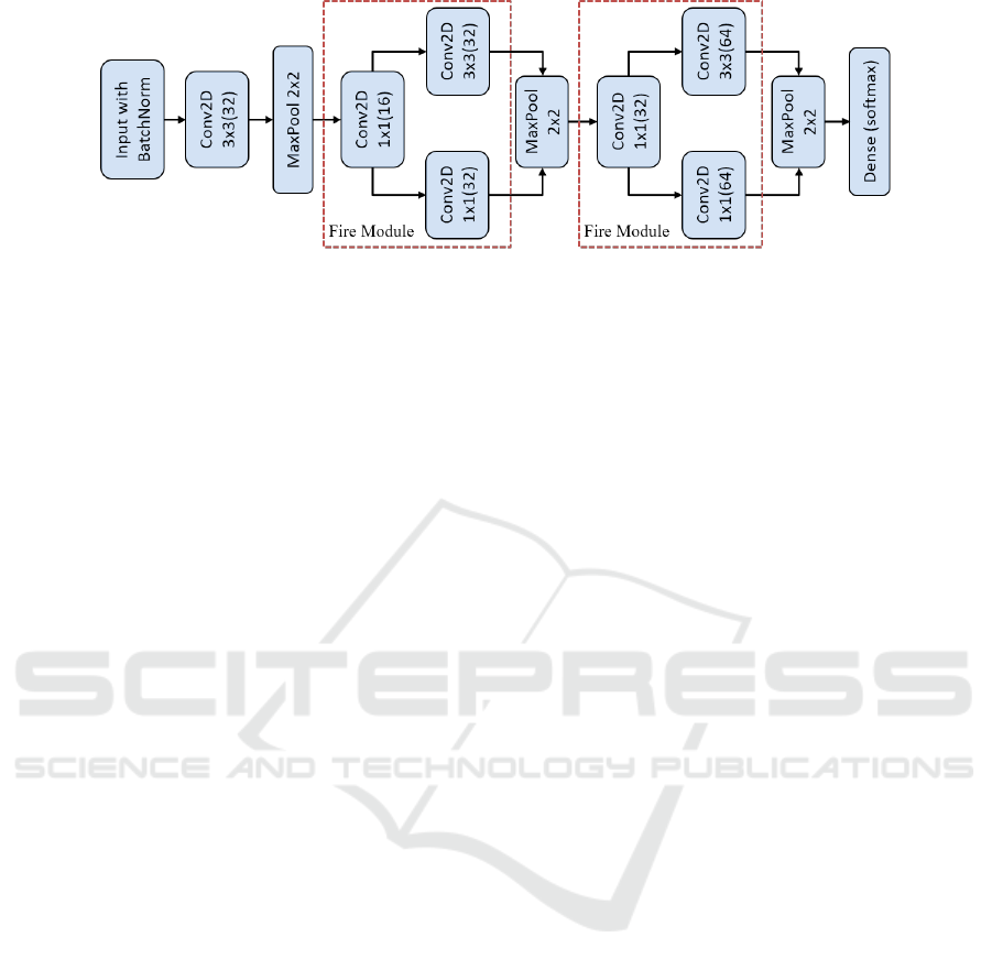
Figure 2: CNN architecture with fire modules from SqueezeNet.
active learning framework with the aim of establish-
ing a minimum overhead for image annotation by the
process engineer along with a high performance and
efficient CNN classifier. An overview of the proposed
framework is summarized in Figure 1. First, an initial
subset of images was manually classified and used to
first train the CNN model. Next, class probabilities
from the output layer are used to estimate the uncer-
tainties and their margin from a new subset of unla-
beled images. Out of this set, a subset of the most
informative and diverse defect images is queried. In
later section we describe in detail, how this subset is
queried based on the uncertainty estimation.
In the next phase, metadata of these images that
contain spatial information of the defects in the wafer
are clustered with DBSCAN algorithm (Schubert
et al., 2017). DBSCAN aims at finding automatically
dense clusters from the data without explicitly assign-
ing the number of the clusters. Initially, it detects the
core points that, within a radius ε, enclose a minimum
number of neighbors minPts. Hence, it reaches the
minimum density in order to form a neighborhood.
The rest of the points, which are not reachable by any
of the core points, are tagged as noisy and they do not
belong to any of the derived clusters. The two former
parameters are critical for the method, as they control
both the number and the structure of the final clusters.
The intuition behind DBSCAN for our case is that
more dense areas on the wafer’s surface constitute a
systematic defect pattern, while less dense areas with
a random arrangement yield noisy instances, which
will be removed from the queried batch of images.
Hence, defect images are mostly included with a spe-
cific map pattern in the level of detail of the wafer
map. Furthermore, the final subset is guided for an-
notation by the process engineer (oracle) and utilized
for updating the CNN model. The process is itera-
tively performed until a maximum number of itera-
tions is reached. Eventually, a significantly smaller
amount of informative images are obtained with the
minimum human effort that will be utilized for train-
ing of the CNN model.
3.2 Classification Model
Extensive research on the field of image recognition
indicated the best fit of deep CNNs for image clas-
sification purposes (Krizhevsky et al., 2012). Since
numerous CNN architectures are available, the de-
sign of the network can be a quite non-trivial task
with many factors to consider, for instance high accu-
racy and optimized real time deployment in embed-
ded devices. Our design architecture was based on
SqueezeNet (Iandola et al., 2016), which combines
AlexNet (Krizhevsky et al., 2012) with Fire modules,
a mixing of compressing and expanding convolutional
layers. First, a squeeze layer resulted from the con-
volution of 1x1 filters will serve as the expand layer
of two convolutional layer with respectively 1x1 and
3x3 filters. Overall, we chose to design a relative
simple, yet powerful multiclass classification model,
by achieving a balance between desired accuracy and
performance. Main advantage of the SqueezeNet ar-
chitecture is the ability to reduce the amount of the
learned parameters, without any compromise on the
accuracy. Small model sizes (<1MB) that result from
such a compact architecture can facilitate their de-
ployment on embedded systems of mobile devices for
real-time defect evaluation right on the wafer inspec-
tion process.
Our deployed CNN architecture of SqueezeNet
is illustrated in Figure 2. Initially, our architecture
begins with a batch normalization layer preceding a
standalone convolutional layer with a filter size of 3x3
and 32 feature maps. Batch normalization technique
is applied on each mini-batch, which can deal with
the issue of covariate shift and the same time accel-
erate training convergence (Ioffe and Szegedy, 2015).
Usually the number of feature maps is increased as
deeper as the network progresses generating more pa-
rameters to learn. To prevent overfitting from the
large amount of learnable parameters, pooling lay-
ers are included to the model by extracting the max-
imum values with the filter size, which in our case
happens to be 2x2. In the middle of our architecture,
KDIR 2020 - 12th International Conference on Knowledge Discovery and Information Retrieval
272

we add two core components of SqueezeNet with in-
creasing number of feature maps, the Fire modules,
which is the key idea of the algorithm for compress-
ing convolutional layers. The compression technique
of SqueezeNet is achieved by a the squeeze layer with
1x1 filters and following an expand layer with a blend
of 1x1 and 3x3 filters.
We emphasize that in wafer fabrication environ-
ments such optimized designs in the architecture
can be of great advantage, since smaller models are
trained faster and hence much more easily deployed
for evaluation right in the production site.
3.3 Enhanced Active Learning
Active learning is mainly considered an improvement
technique in machine learning, as it aims at select-
ing for training those subsets of data that will help
the predictive model to perform and generalize bet-
ter. Since labelling of instances is both a tedious and
a costly task, active learning can play a pivotal role,
as with less training data better classification accuracy
is achieved. Main ingredient of such methods is the
estimated uncertainty, which is usually derived from
the softmax output values of the CNN model that rep-
resent the probabilities of each individual predicted
class. Although existing alternatives are available for
quantifying the uncertainty, such as least confidence
or entropy (Settles and Craven, 2008), (Hwa, 2004),
we employ the least margin approach (Scheffer et al.,
2001) to estimate the uncertainty, which is the differ-
ence of the largest output probability with the second
largest output probability.
In the following part of the section we introduce
the active learning algorithm that we employ for our
framework with the necessary notation. Let D =
{X
i
}
N
i=1
be the whole dataset with N the total num-
ber of the images, X
i
∈ R
px×px
the image matrix of
pixel size px × px. Including the label vector y
i
for
i-th image X
i
, we denote a labeled set D
L
⊂ D that is
used for training the CNN model. Similarly, an unla-
beled set denoted by D
U
⊂ D will be queried by the
proposed algorithm to further filter out all the unim-
portant noisy images. At the end step, the CNN model
is updated by the enhanced dataset Q.
For each image i, the model outputs the softmax
probability p
j
with j ∈ {1, .. . ,C}, where C the num-
ber of classes. Hence the least margin of a i-th image
is calculated as follows.
lm
i
= p
j1
(X
i
, y
i
) − p
j2
(X
i
, y
i
) (1)
where j
1
and j
2
represent the first and second most
probable output classes from the CNN model. The
margins are mainly utilized to form a weighted clus-
tering via a density based technique.
We further utilize the metadata information for ev-
ery defect image from each wafer, that constitutes an
additional dataset M = {w
i1
, w
i2
, w
i3
}
N
i=1
, where w
i1
,
w
i2
, w
i3
the spatial Cartesian coordinates of the defect
images on the wafer and its identification number, re-
spectively. Compactly, denoted by {w
i
}
N
i=1
. Algo-
rithm 1 presents in detail the pseudocode of the entire
framework.
Algorithm 1: Pseudocode for proposed system.
Input : Datasets D, M ,
initial size of labeled dataset N
1
,
query size per repetition N
2
,
maximum size N
L
of labeled set
Output: Enhanced labeled dataset Q
1 D
L
← random sample from D of size N
1
2 Annotate images from D
L
3 D
U
← D \ D
L
4 Train CNN model with D
L
5 Initialize k ← 1
6 while k < N
L
do
7 Query most uncertain images from D
U
8 Q ← most uncertain images
9 Apply DBSCAN on set {w
i
;i ∈ Q}
10 Set P with images out of dense
neighborhood
11 Update queried set Q ← Q \ P
12 k ← k +1
13 Train CNN model with Q
14 end
4 EXPERIMENTS
4.1 Preprocessing
We introduced five defect classes, with their sizes,
for our classification task: dc1 (8791), dc2 (12135),
dc3 (3951), dc4 (3912), and dc5 (145). Common de-
fects might be stain, cracks, etc. The dataset con-
sisted in total of 28,935 images from 1073 unique
wafers. Each image file name was accompanied with
its metadata information, which incorporates wafer id
and spatial coordinates of the chip defects. In order to
alleviate the high imbalance in the dataset, we apply
class weights during training to the loss function of
cross entropy. Defect class with code dc3 comprises
images with higher intra-class variance, which they
don’t belong neither to the rest of the classes.
To establish the appropriate image size for the
overall defect classification scheme, we introduce a
preprocessing step of the image dataset. With regard
Enhanced Active Learning of Convolutional Neural Networks: A Case Study for Defect Classification in the Semiconductor Industry
273
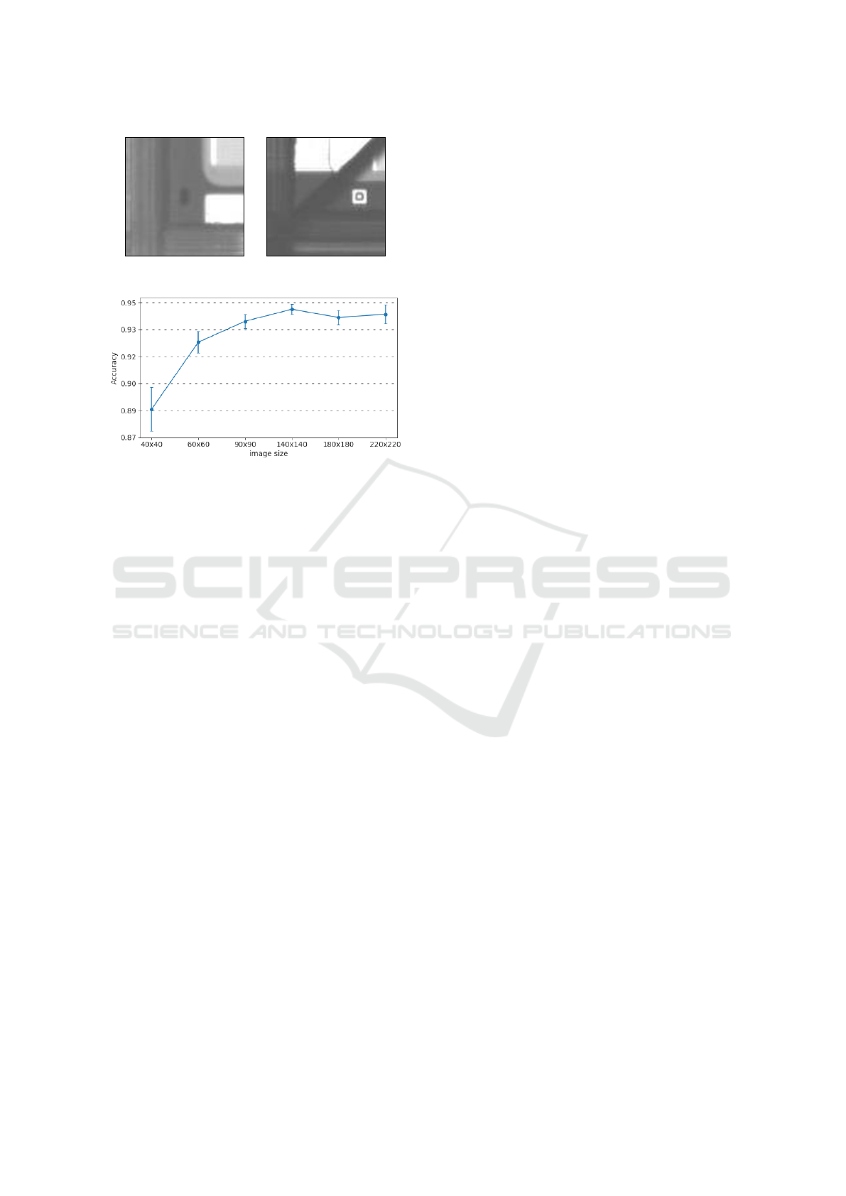
Figure 3: Sample images of two types of chip defects.
Figure 4: Accuracy versus cropped image sizes in pixels.
to the image size, two essential criteria should be ful-
filled. First, the entire defect’s structure must be in-
cluded as well as centered in the image, with the con-
straint that only the affected die is captured without
any neighboring ones. Second, the final size needs to
be at least twice the width of the chip separating bor-
derlines, so that the defect is more distinguishable for
the classification task.
Figure 3 illustrates two defected die images of size
90x90 pixels with their borderlines on the wafer. In
case the borderlines are dominating the image, con-
fusion to the final classification is increased and re-
spectively performance will be severely affected. We
carried out a 5-fold cross validation for the evaluation
of the performance accordingly to each cropped im-
age size as shown in Figure 4. Additional insight for
the final decision of the image size was provided from
the process engineer as well, as a size of 90x90 pixels
can include a chip defect within the die with an ample
buffer. In addition, the Elbow Method (Ketchen and
Shook, 1996) on the accuracy diagram provided us a
further hint about the final decision on the image size
for the dataset to achieve a trade-off with classifica-
tion performance.
4.2 Experimental Design
We embody our active learning algorithm with the
Squeezenet architecture of the CNN model. Initially,
we kept out in total 20,182 images as a test set with
the following distribution of classes: dc1 (6113), dc2
(8495), dc3 (2722), dc4 (2773), and dc5 (79). The
rest 8,753 defect images were used to build the train-
ing set. For the needs of our experiments, we assume
that the images in the training set are unlabeled, from
which at every iteration of the algorithm a subset is
queried for annotation from the expert. Hence, the
validation of the expert on the class labels is already
incorporated into the examined dataset, in order to be
able to properly conduct the evaluation process.
The effectiveness of our proposed method with
the CNN is evaluated, by comparing it with other
two widely known classification algorithms, support
vector machine (SVM) and multi-layer perceptron
(MLP). Initially, we conducted a 5-fold cross vali-
dation to obtain the optimal values of the hyperpa-
rameters for the former methods. More specific, for
the SVM we used the radial basis function kernel
with a regularization parameter 1/100, while for the
MLP, we deploy three layers with 64, 128, 64 hid-
den units, respectively. Moreover, we select the rec-
tified linear unit (ReLU) as an activation function in
the hidden layers for the MLP, which in practice has
proven to outperform other more complex functions
(Ramachandran et al., 2017). Both machine learn-
ing packages are implemented in (Pedregosa et al.,
2011). Besides SVM and MLP classification meth-
ods, we further consider the full approach as a base-
line method, in which the CNN model is trained over
the entire training set without any active learning
scheme.
To further evaluate and properly quantify the over-
all performance of all methods, we consider four
widely used measures, accuracy, precision, recall and
f1-score. The three performance measures are calcu-
lated as follows.
• Accuracy: the ratio of the correctly classified de-
fect images to the total number of images.
• Precision: the ratio of correctly classified images
for each defect class to the total number of images
that were predicted to be of each specific defect
class.
• Recall: the ratio of correctly classified images for
each defect class to the total number of images
that were actually of a specific defect class.
F1-score is the harmonic average of the precision and
recall and in practice it is a quite useful metric.
For training the CNN classifier, an Adam opti-
mizer was employed with a learning rate of 0.001
and a batch size of 32 for 10 training epochs. Gener-
ally, for multi-class classification problem the cross-
entropy cost function is optimised during gradient de-
scent algorithm. In order to obtain all class proba-
bilities, we applied the softmax activation function to
the output layer of the network, which we also used
KDIR 2020 - 12th International Conference on Knowledge Discovery and Information Retrieval
274

for estimating the prediction’s uncertainty from the
queried subset.
We initialized our active learning system with 200
labeled images, randomly sampled from the training
set with a stratified manner. We set all images in the
training set as the limit of the total iterations of the al-
gorithm. A subset size of 128 images is first queried
based on least margin estimations during each itera-
tion. By utilizing spatial metadata of the queried sub-
set Q, DBSCAN clustering was conducted on each
wafer. Based on production requirements on the ex-
isting wafer fabrication line, we set 5 data points as
the minimum size of a dense neighborhood minPts
with a minimum radius ε of 10. Any point that is not
reachable within a dense neighborhood, constitutes a
systematic wafer defect and is removed from the set
Q. The iterative process continues until no other train-
ing data are available for querying.
4.3 Results and Discussion
Figure 5 shows the comparison results of the baseline
classifiers with the CNN model, which they are all in-
tegrated into the active learning framework. Evalua-
tion is performed with the images from the test set,
that were held out from the training process and a
weighted average of F1-score is calculated. As shown
in the figure, at the 15th active learning iteration the
performance of the CNN model generally converges
and clearly outperforms the other two methods, even
at the beginning of the iterations. SVM performs
worse than the CNN model and slightly better than
the MLP, as it can handle better cases with D N,
where D and N the number of dimensions and sample
size, respectively. However, a better performance of
SVM comes with a higher computational cost in both
training and predicting as the number of sample size
is incrementally increasing. Similarly as CNN, MLP
starts to converge in a later time as the network needs
more images to learn the underlying data distribution.
Overall, the number of the iterations towards conver-
gence amounts to < 1,900 labeled images which is
significant less than the number of the total images
that we initially set as the upper limit of the iterations.
Table 1 summarizes the classification results for
the enhanced active learning with all classifiers as
well as the training of the CNN model with the full
set of the training data, respectively. Enhanced CNN
with active learning reported superior performance, in
terms of the average of accuracy, precision and recall.
In contrast, CNN that is trained with the entire dataset
achieves better performance than MLP, yet with a
higher labelling and computational cost. Although,
SVM with active learning performs evenly good with
Figure 5: Overall classification performance with F1 score
versus the iterations of the active learning system. At 26th
iteration F1 score seems to converge for all methods. Any
class imbalance is taken into account by weighted average
for each class label.
the full CNN, training of the former is by far the most
computationally intensive of all other competitors.
Table 1: Final performance comparison of proposed method
with averaged values over all defect classes on the test set.
Values are not weighted by the number of true instances for
each class label.
Method Accuracy Precision Recall
MLP 0.920 0.823 0.772
SVM 0.939 0.889 0.792
CNN (enhanced) 0.956 0.938 0.849
CNN (full) 0.925 0.897 0.796
5 CONCLUSION
In this study we propose an iteratively active learn-
ing framework of a convolutional neural network in
a real wafer manufacturing process. We employ a
SqueezeNet CNN architecture that best fits the needs
for an optimized deployment of our system, as the fi-
nal prediction model barely exceeds a size of 1MB. A
preprocessing step is preceded in order to determine
the most appropriate image size of the chip defects for
our classification purposes. At the first stage, most in-
formative and diverse defect images are queried based
on uncertainty estimation that derived from the soft-
max output probabilities. The queried subset, at the
second stage, is further enhanced by dropping noisy
instances via a weighted density-based clustering al-
gorithm with the spatial metadata information. Our
experiments show that our active learning system out-
performed the full model with an ample margin as
well as other classification algorithms. With the pro-
posed system, not only we improved the classification
performance but less effort and time is invested by the
process engineer for labelling the chip defect images.
As future work, we will explore the incorporation
Enhanced Active Learning of Convolutional Neural Networks: A Case Study for Defect Classification in the Semiconductor Industry
275

of other sources of heterogeneous data from the wafer
fabrication line, such as text, in order to further re-
duce the annotation cost by partially automating the
process. Also, we are interested in developing novel
criteria for querying the most informative instances in
the dataset that will lead to more robust and accurate
predictive models.
ACKNOWLEDGEMENTS
This work has been supported by Pro
2
Future (FFG
under contract No. 854184). Pro
2
Future is funded
within the Austrian COMET Program -Competence
Centers for Excellent Technologies- under the aus-
pices of the Austrian Federal Ministry of Trans-
port, Innovation and Technology, the Austrian Fed-
eral Ministry for Digital and Economic Affairs and of
the Provinces of Upper Austria and Styria. COMET
is managed by the Austrian Research Promotion
Agency FFG. Tiago Santos was a recipient of a DOC
Fellowship of the Austrian Academy of Sciences at
the Institute of Interactive Systems and Data Sci-
ence of the Graz University of Technology. Michael
Wiedemann was with TDK Electronics, Austria and
now with RF360 Europe GmbH, Germany. Stefan
Thalmann is with the University of Graz and Graz
University of Technology, Graz, Austria.
REFERENCES
Cheon, S., Lee, H., Kim, C. O., and Lee, S. H. (2019).
Convolutional neural network for wafer surface de-
fect classification and the detection of unknown defect
class. IEEE Transactions on Semiconductor Manufac-
turing, 32(2):163–170.
Chou, P. B., Rao, A. R., Sturzenbecker, M. C., Wu, F. Y.,
and Brecher, V. H. (1997). Automatic defect classi-
fication for semiconductor manufacturing. Machine
Vision and Applications, 9(4):201–214.
Huang, S.-H. and Pan, Y.-C. (2015). Automated visual
inspection in the semiconductor industry: A survey.
Computers in industry, 66:1–10.
Hwa, R. (2004). Sample selection for statistical parsing.
Computational linguistics, 30(3):253–276.
Iandola, F. N., Han, S., Moskewicz, M. W., Ashraf, K.,
Dally, W. J., and Keutzer, K. (2016). Squeezenet:
Alexnet-level accuracy with 50x fewer parameters and
< 0.5 mb model size. arXiv preprint.
Ioffe, S. and Szegedy, C. (2015). Batch normalization: Ac-
celerating deep network training by reducing internal
covariate shift. arXiv preprint.
Ketchen, D. J. and Shook, C. L. (1996). The application of
cluster analysis in strategic management research: an
analysis and critique. Strategic management journal,
17(6):441–458.
Krizhevsky, A., Sutskever, I., and Hinton, G. E. (2012). Im-
agenet classification with deep convolutional neural
networks. In Advances in neural information process-
ing systems, pages 1097–1105.
Kyeong, K. and Kim, H. (2018). Classification of mixed-
type defect patterns in wafer bin maps using convolu-
tional neural networks. IEEE Transactions on Semi-
conductor Manufacturing.
Nakazawa, T. and Kulkarni, D. V. (2018). Wafer map defect
pattern classification and image retrieval using convo-
lutional neural network. IEEE Transactions on Semi-
conductor Manufacturing, 31(2):309–314.
Pedregosa, F., Varoquaux, G., Gramfort, A., Michel, V.,
Thirion, B., Grisel, O., Blondel, M., Prettenhofer, P.,
Weiss, R., Dubourg, V., et al. (2011). Scikit-learn:
Machine learning in python. the Journal of machine
Learning research, 12:2825–2830.
Ramachandran, P., Zoph, B., and Le, Q. V. (2017).
Searching for activation functions. arXiv preprint
arXiv:1710.05941.
Rawat, W. and Wang, Z. (2017). Deep convolutional neural
networks for image classification: A comprehensive
review. Neural computation, 29(9):2352–2449.
Scheffer, T., Decomain, C., and Wrobel, S. (2001). Active
hidden markov models for information extraction. In
International Symposium on Intelligent Data Analy-
sis, pages 309–318. Springer.
Schubert, E., Sander, J., Ester, M., Kriegel, H. P., and Xu,
X. (2017). Dbscan revisited, revisited: why and how
you should (still) use dbscan. ACM Transactions on
Database Systems (TODS), 42(3):1–21.
Settles, B. (2009). Active learning literature survey. Techni-
cal report, University of Wisconsin-Madison Depart-
ment of Computer Sciences.
Settles, B. and Craven, M. (2008). An analysis of active
learning strategies for sequence labeling tasks. In Pro-
ceedings of the 2008 Conference on Empirical Meth-
ods in Natural Language Processing, pages 1070–
1079.
Shim, J., Kang, S., and Cho, S. (2020). Active learn-
ing of convolutional neural network for cost-effective
wafer map pattern classification. IEEE Transactions
on Semiconductor Manufacturing, 33(2):258–266.
Wang, K., Zhang, D., Li, Y., Zhang, R., and Lin, L. (2016).
Cost-effective active learning for deep image classi-
fication. IEEE Transactions on Circuits and Systems
for Video Technology, 27(12):2591–2600.
KDIR 2020 - 12th International Conference on Knowledge Discovery and Information Retrieval
276
