
Terahertz Transmission Through Patterened Vanadium Oxide Thin
Films on Dielectric Substrates
M. Akkaya
1
, Y. Demirhan
2
, H. Yuce
2
, G. Aygun
2
, L. Ozyuzer
2
, C. Sabah
3
and H. Altan
1
1
Department of Physics, Middle East Technical University, 06800, Çankaya Ankara, Turkey
2
Department of Physics, Izmir Institute of Technology, 35430, Urla, Izmir, Turkey
3
Department of Electrical and Electronics Engineering, Middle East Technical University- Northern Cyprus Campus
(METU-NCC), 99738, Kalkanlı, Güzelyurt, TRNC / Mersin 10, Turkey
Keywords: Terahertz (THz), Time Domain Spectroscopy (TDS), Vanadium Dioxide (VO
2
).
Abstract: Patterned and unpatterned films of vanadium oxide grown on dielectric substrates such as fused silica and
sapphire were grown and analysed by varying the temperature using terahertz time domain spectroscopy.
After investigating the critical transition temperature near 340K, a well-known cross-shaped pattern was
studied to observe any resonances upon transmission. Due to the poor conductivity of the films the
frequency selective nature of the structure was not observed, however an etalon effect could be seen in the
sapphire substrate as opposed to the fused silica substrate above the critical temperature. Dependence of the
refractive index difference between substrates upon transmission of the THz pulse is likely in explaining
this observed difference.
1 INTRODUCTION
In the electromagnetic (EM) spectrum, the region
between Microwave and Infrared Region
corresponds to Terahertz (THz) frequency range
(Zhang, 2010). This range corresponds to 10
12
hertz
in the spectrum. Generally, this radiation is called T-
rays. T-rays have 4.1 meV energy at 1 THz, an
equivalent temperature of 48 K, period of 1 ps,
wavelength of 300 μm and a corresponding wave
number of 33.3 cm
-1
(Lee, 2009). THz region has a
variety of advantages since it falls within reach of
both electronics and optics. Therefore, in THz region
both technologies are important to generate or to
detect THz radiation. Development of time domain
terahertz spectroscopic techniques is one of the most
successful of THz applications. By using terahertz
time domain spectroscopy (THz-TDS), scientists
have been able to successfully characterize
dielectrics, semiconductors and also superconductors
(Grischkowsky, 1990).
It is important to create technologies which can
both control the frequency and amplitude or
intensity of the radiation in this region. Due to the
low energy of these photons it has been a challenge
to create devices which work in this frequency range
at room temperature. Metamaterials or frequency
selective surfaces offer a method to control the
transmission or reflection of terahertz waves in and
around the frequency region of interest (Holloway,
2005). Since terahertz radiation is highly reflected
by conducting materials recent efforts have
concentrated on developing smart materials which
can change their conductivity upon a change in a
parameter which can be controlled externally.
Typically this externally controlled parameter can
either be temperature, applied bias or current.
Studies have been done with semi and
superconducting metasurfaces (Chen, 2006). While
superconducting metamaterials have been shown to
change the transmission or reflection of terahertz
radiation significantly in a narrow bandwidth their
commercial use is complicated by the cooling
requirements and the power necessary to drive these
systems. A device that can show efficient tunability
over a broad or narrow bandwidth that operates near
room temperature has yet to be demonstrated.
Development of smart materials which exhibit a
phase transition at or near room temperature will
provide the necessary solution to this problem.
Offering similar behavior under external control,
few studies have been done on room temperature
insulators such as Vanadium Oxide (VO
2
) which
334
Akkaya M., Demirhan Y., Yuce H., Aygun G., Ozyuzer L., Sabah C. and Altan H.
Terahertz Transmission Through Patterened Vanadium Oxide Thin Films on Dielectric Substrates.
DOI: 10.5220/0006268703340339
In Proceedings of the 5th International Conference on Photonics, Optics and Laser Technology (PHOTOPTICS 2017), pages 334-339
ISBN: 978-989-758-223-3
Copyright
c
2017 by SCITEPRESS – Science and Technology Publications, Lda. All rights reserved

shows metallic behavior at high temperatures
(Jepsen, 2006).
Vanadium dioxide’s (VO
2
)
conductivity is of
particular interest since its conductivity changes
when the temperature is changed, exhibiting a phase
transition. Its phase changes from an insulator
(semiconductor) to metallic state when the
temperature increases above a value typically near
340K (Liu, 2012). By using different deposition
techniques, VO
2
films have been grown on sapphire,
quartz, silicon, etc. (Wang, 2005). Jepsen et al.
investigated that VO
2
on the sapphire substrate is
transparent for THz radiation when the temperature
is below the transition temperature and therefore it is
in the insulator state. However, for nominally high
temperatures such as above the transition
temperature, VO
2
on the sapphire substrate reflects
the THz radiation since it is in the metallic state.
In this study, by using a home-built THz-TDS
system, the transmission of the THz radiation was
investigated for grown thin films of Vanadium
dioxide (VO
2
) on different dielectric substrates at
different temperatures. After detection of the metal-
insulating transition point, grown films were etched
and patterned in order to investigate the frequency
selective nature of the surface.
2 MEASUREMENTS
2.1 Terahertz Time Domain
Spectroscopy
Vanadium dioxide (VO
2
) patterned and unpatterned
films were characterized using a home-built THz-
TDS system. The system utilizes a Photoconductive
Antenna (PCA) in generation and electro-optic
sampling in detection. A femtosecond Ti:Sapphire
mode-lock laser source is used in order to generate
and detect the THz radiation. The laser has a 75
MHz repetition rate, 16fs pulse width and 800 nm
central wavelength. In this system a beam splitter is
used in order to split the output beam of the laser
into generation and detection arms. Its transmission
ratio is 95:5. The THz signal is detected using
electro-optic detection through a 2mm thick <110>
oriented ZnTe crystal. A balanced photodiode, lock-
in amplifier synced to the function generator driving
the modulation on the photoconductive antenna and
a personal computer are used to record the THz
waveforms.
The THz radiation is generated in a
commercially obtained PCA which is modulated at 1
kHz and biased at +/-15V. Afterwards the generated
radiation is collected with the aid of a silicon lens,
the THz waves are then collimated by an off-axis
parabolic mirror. Then, by using a converging TPX
lens, the THz radiation is focused on to the sample
in order to have efficient sample-THz interaction.
Next, another TPX lens is used in order to collimate
the diverging THz beam. Then, by using another off
axis parabolic mirror, this beam is collected and
focused through onto the ZnTe crystal.
Figure 1: Schematic representation of THz-TDS system.
In the detection arm, the beam is directed onto a
corner cube on the top of the translational stage
which is used to scan the electric field of the THz
waveform. The THz waveform is collected by
stepping the stage through the waveform. The
femtosecond visible pulse polarization changes as it
passes though the electro-optic set-up for different
values of the THz electric field. The entire system is
controlled using LabView software.
2.2 Closed Cycle Cryostat
In order to control the temperature during the THz
measurements a closed cycle cryostat was used
which was already in place to perform low
temperature measurements on different samples. The
system was used in heating mode only and in order
to increase and control the temperature starting from
room temperature to higher temperatures a
temperature controller is used. This system consists
of Sumitomo CH-204SFF coldhead and Vacuubrand
RZ14 vacuum pump. At the end of the cold head
there is a sample holder and sample is mounted
there. Also, THz radiation is transmitted through the
sample after passing through quartz windows placed
around the cold head.
Terahertz Transmission Through Patterened Vanadium Oxide Thin Films on Dielectric Substrates
335
2.3 VO
2
In this study the measurements were done for three
samples: unpatterned VO
2
on the sapphire substrate,
cross shape patterned VO
2
on the top of both
sapphire and fused silica substrates.
VO
2
thin films with a thickness of ~250 nm were
deposited on c-cut sapphire (500 ߤm thick) and
fused silica (900 ߤm thick) substrates by dc
magnetron sputtering in 98.5% Ar + 1.5% O
2
environment. 2" high purity (99.95%) vanadium (V)
was used as sputtering target. VO
2
films were
fabricated under the same growth conditions for both
sapphire and fused silica substrates. Before the
substrates were placed into vacuum chamber, these
substrates were ultrasonically cleaned in acetone,
methanol and propanol for 10 min, respectively.
Then, the substrates were dried with pure nitrogen
flow. The base pressure in sputtering chamber was
below 1.6x10
-6
Torr, and deposition pressure in the
chamber was 8.3x10
-3
Torr. To remove
contaminations from the surface of V target, 10 min
pre-sputtering was carried out. Dc power of 50 W
was applied to V target. Substrates were heated up to
550
o
C, and this substrate temperature was kept
constant during deposition. In addition, in order to
improve homogeneity on the film surface, each
substrate was rotated at 15 rpm.
To understand the quality of the grown films, the
critical temperature and conductive properties of
unpatterned VO
2
was initially analyzed by using
THz-TDS system with the closed cycle cryostat
shown above.
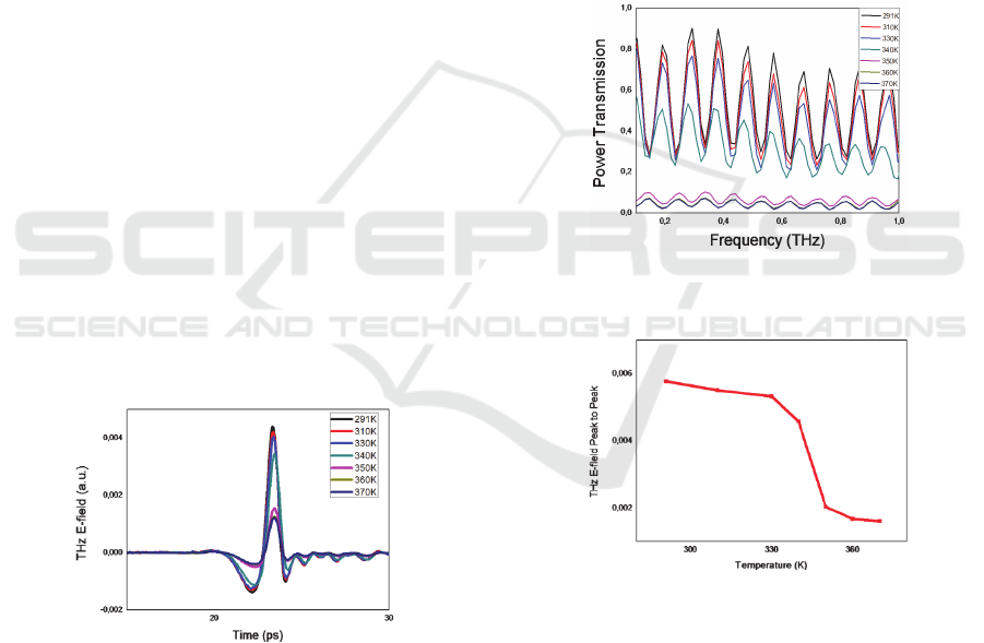
Figure 2: THz E-field vs. time graph for unpatterned
250nm thick VO
2
film on sapphire substrate.
In Figure 2 it can be noticed that when VO
2
changes between the insulating and the metallic
state, amplitude of the electric field of the
transmitted wave varies significantly. In Figure 3
this change is shown with respect to frequency after
applying a Fourier transform on the time-dependent
waveforms. The oscillations are due to the etalon
effect which becomes more prominent with increase
of temperature. This is more evident when the
critical temperature of the VO
2
sample is above
340K. Moreover, it can be said that when the
temperature is below the critical temperature the
sample is an insulator and when the temperature is
above the critical temperature the sample is metallic
and there it reflects the THz radiation adding to the
observed dips in the etalon. Also, in Figure 4, the
THz electric field peak to peak value is plotted with
respect to temperature, showing this transition
clearly. Therefore, these results are in agreement
with the works published previously (Jepsen, 2006).
After confirming the critical temperature of VO
2
,
similar films grown on fused silica and sapphire
substrates were patterned to investigate the
frequency selectivity of the films under changing
temperature.
Figure 3: Power transmission vs. frequency graph for
unpatterned 250nm thick VO
2
film on sapphire substrate.
Figure 4: THz E-field peak to peak with respect to
temperature for unpatterned 250nm thick VO
2
film on
sapphire substrate.
2.4 Frequency Selective Surfaces
In this study, a cross shape (Demirhan, 2016) pattern
was investigated for VO
2
films on sapphire and
fused silica substrates. The cross shape patterns were
obtained by employing photolithography, and ion
beam etching techniques. In Figure 5, the
dimensions of the cross shape patterned VO
2
on
dielectric substrate can be seen.
PHOTOPTICS 2017 - 5th International Conference on Photonics, Optics and Laser Technology
336
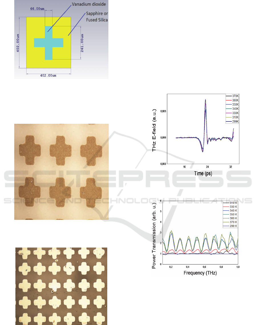
Figure 5: Front view and dimensions of the cross shaped
VO
2
unit cell.
Moreover in Figure 6 and Figure 7 the optical
microscope images of cross shape patterned VO
2
on
sapphire and fused silica substrates is shown.
Figure 6: Optical microscope image of 250nm thick VO
2
frequency selective surface on sapphire substrate. The
dark areas are VO
2
.
Figure 7: Optical microscope image of 250nm thick VO
2
frequency selective surface on fused silica substrate. The
dark areas are VO
2
.
3 RESULTS
3.1 Cross Shaped VO
2
on Sapphire
Substrate
First, the cross shaped VO
2
on the sapphire substrate
is measured using the THz TDS system. In Figure 8
the THz electric field with respect to time can be
seen. In Figure 9 the power transmission with
respect to the frequency is shown. In this figure the
transmission at 299K (initial temperature) was
referenced to the transmission at different
temperatures.
Figure 8: THz E-field vs. time graph for cross shape
patterned VO
2
for sapphire substrate.
Figure 9: Power transmission with respect to frequency for
cross shape patterned VO
2
on sapphire substrate.
3.2 Cross Shaped VO
2
on Fused Silica
Substrate
Second, the cross shaped VO
2
on the fused silica
substrate is measured using the THz TDS system.
The THz electric field with respect to time and
power transmission with respect to frequency can be
seen in Figure 10 and 11, respectively. In Figure 11
the transmission at 299K (initial temperature) is
Terahertz Transmission Through Patterened Vanadium Oxide Thin Films on Dielectric Substrates
337
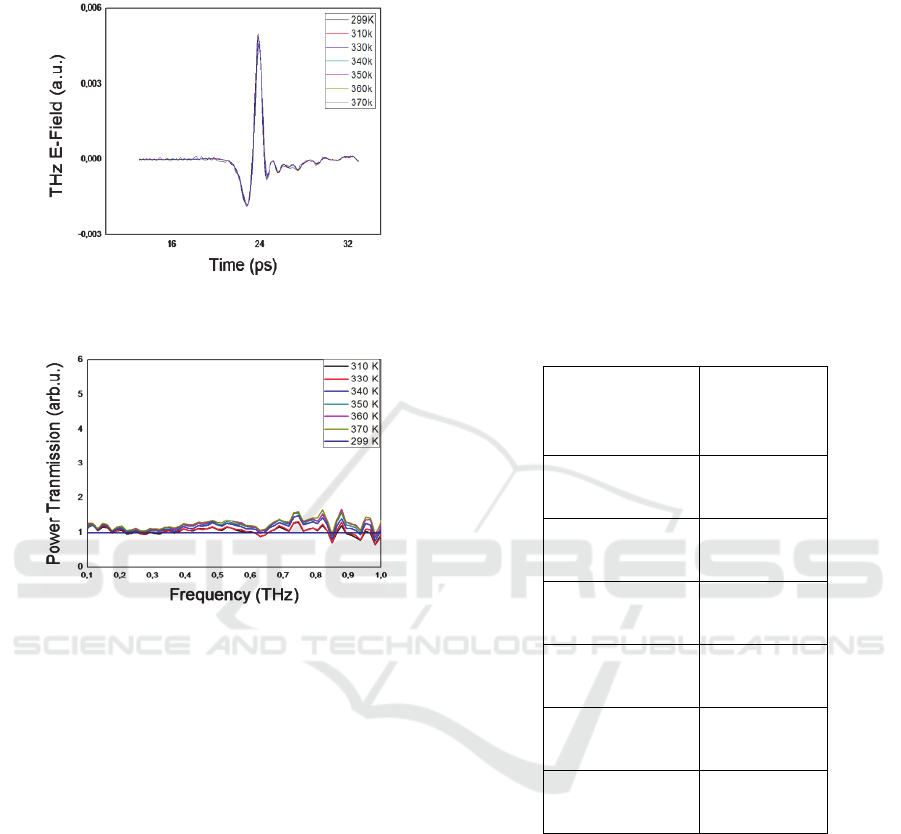
referenced to the transmission at different
temperatures.
Figure 10: THz E-field vs. time graph for cross shape
patterned VO
2
on fused silica substrate.
Figure 11: Power transmission vs. frequency graph for
cross shape patterned VO
2
on fused silica substrate.
3.3 Analysis
The critical temperature of unpatterned VO
2
is found
to be approximately at 340K. This is also evident in
the behaviour of the electric field of the incoming
THz wave which varies significantly near here. In
addition, the unpatterned VO
2
sample is in the
metallic state when the temperature is above the
critical temperature, and it reflects the THz
radiation. Similarly, below the critical temperature,
sample is in the insulating state and it is more
transparent to the incoming THz radiation.
For the patterned samples, examining Figure 9
the sample is in a more metallic state as the
temperature is increased and interestingly enough in
this state etalon effects can be observed which also
becomes prominent with increase in temperature. In
contrast, for the patterned cross shape VO
2
on fused
silica substrate (Figure 11) the etalon effects are not
apparent. In Figure 8 and Figure 10 both power
transmissions are normalized to transmission at
higher temperatures. Hence the ratio is expected to
be greater than 1 since the 299K state is more
transparent.
The etalon effect in Figure 8 can be analysed to
understand the thickness or refractive index of the
substrate. The refractive index of sapphire substrate
at different temperatures can be calculated using;
∆f=c/2nd (1)
In this formula c is the speed of light in mm and
d is the thickness of sapphire substrate and it is equal
to 0.5 mm. The peak difference of the frequency
value can be calculated by using Figure 9, this value
is measured as 0.103 THz. The calculated real
refractive indices for different temperatures are
shown in Table 1.
Table 1: Calculated Real Refractive index of sapphire at
different temperatures.
Temperature
(K)
Refractive
index
310 2,93
330 2,93
340 2,93
350 2,93
360 2,93
370 2,93
This table shows that refractive index of sapphire
does not change when the temperature is increased
and according to this calculation its refractive index
is approximately 2.93. Previous measurements have
shown that the refractive index of sapphire is nearly
3.00 (Lee, 2009).
In cross shaped VO
2
on fused silica substrate, the
etalon effects are not apparent. The thickness of the
fused silica substrate is greater than the sapphire
substrate and also refractive index of fused silica is
smaller than the refractive index of sapphire
substrate. Therefore, etalon effects are not seen in
fused silica substrate. To explain this, one can
examine the difference in refractive index.
Refractive of sapphire is approximately 3 and
PHOTOPTICS 2017 - 5th International Conference on Photonics, Optics and Laser Technology
338

refractive index of fused silica is approximately 2
(Lee, 2009). Therefore when we compare percentage
of power reflection from one interface between these
substrates, in sapphire it is ~%25 and in fused silica
it is ~%11. In order to see etalon effect, there should
be interference and in fused silica this is lower than
that of the sapphire substrate as one interface
becomes more metallic.
4 CONCLUSION
In this study the transmission of THz radiation is
investigated through patterned and unpatterns films
of VO
2
grown on dielectric substrates using THz-
TDS. The critical temperature for a VO
2
film
thickness of 250nm on sapphire substrate is
observed to be close to the accepted value of 340K.
Above this critical temperature unpatterned VO
2
is
in the metallic state and it reflects THz radiation.
However, below the critical temperature,
unpatterned VO
2
is in the insulating state and it is
transparent for THz radiation. After patterning the
films deposited on both fused silica and sapphire
substrates using a well-known cross shape frequency
selective surface pattern the experiments were
repeated to observe the frequency selectivity of the
devices. Due to the small change in conductivity
between insulator and metallic states the frequency
selective properties of the patterned VO
2
surface was
not observed as was expected if the surface was a
pure metallic conductor. While frequency selectivity
was not observed, the change in conductivity with
temperature was enough to result in an etalon effect
which became more evident with increasing
temperature for the sapphire substrate sample and
not the fused silica substrate sample. The
preliminary analysis indicates that the observation of
this etalon effect in the sapphire case and not the
fused silica case is most likely due to the difference
in refractive index between the two substrates.
While one surface reflects more for one substrate the
other surface becomes equally more metallic as the
temperatures increases for both substrate samples.
Future studies will focus on increasing the
quality of the VO
2
deposited samples and
understanding why any resonance was not observed.
The frequency selective nature of the surface failed
due most likely to the low conductivity of the film.
Previous studies done by our group show that low
conductivity in metallic films can result in a
decrease in the observed resonance expected with
frequency selective surfaces (Demirhan, 2016).
Using a commercial software such as CST
Microwave Studio further work will focus on
simulating the transmission of the THz pulse
through the VO
2
patterned film on both dielectric
substrates.
ACKNOWLEDGMENTS
This project was supported in part by METU
research office funded grant BAP-08-011-2016-053.
Hakan Altan also acknowledges support from
BAGEP Award of the Science Academy in Turkey
and also the support of the Turkish Academy of
Sciences in the framework of the Young Scientist
Award Program (TUBA-GEBIP).
REFERENCES
X. C. Zhang, and J. Xu 2010. “Introduction to THz Wave
Photonics” Springer Science+Business Media, LLC.
Y. S. Lee 2009. “ Principles of Terahertz Science and
Technology” Springer Science+Business Media, LLC.
D. Grischkowsky, S. Keiding, M. Exter and C. Fattinger
1990. J. Opt. Am. B/Vol.7 No.10/October 1990
C. L. Holloway, M. A. Mohamed, E. F. Kuester, and A.
Dienstfrey 2005. IEEE Transcations on
Electromagnetic Compatibility, 47(4):853-865, Nov
2005.
H. T. Chen, W. J. Padilla, J. M. O. Zide, A. C. Gossard, A.
J. Taylor, R. D. Averitt 2006. Nature 444,597-600.
P. U. Jepsen, B. M. Fischer, A. Thoman, H. Helm, J. Y.
Suh, R. Lopez and R. F. Haglund 2006. Phys. Rev B
74, 205103.
M. Liu, H. Y. Hwang, H. Tao, A. C. Strikwerda, K. Fan,
G. R. Keiser, A. J. Sternbach, K. G. West, S.
Kittiwatanakul, J. Lu, S. A. Wolf, F. G. Omenetto, X.
Zhang, K. A. Nelson and R. D. Averitt 2012. Nature
487. doi:10.1038/nature11231.
H. Wang, X. Yi, S. Chen, X. Fu 2005. Sensors and
Actuators A 122 (2005) 108-112.
Y. Demirhan, H. Alaboz, L. Ozyuzer, M. A. Nebioglu, T.
Takan, H. Altan, C. Sabah 2016. Optical and Quantum
Electronics, 48(2):1-11.
Terahertz Transmission Through Patterened Vanadium Oxide Thin Films on Dielectric Substrates
339
