
Capacity Analysis of Radio Frequency Interconnect for
Manycore Processor Chips
Eren Unlu, Christophe Moy, Yves Louet and Jacques Palicot
CentraleSupelec-IETR, F-35576 Cesson-Sevigne Cedex, France
eren.unlu@supelec.fr
Keywords: Capacity analysis, Manycore processor chip, OFDMA.
Abstract: We study here the case of a 2048 cores chip, where cores are spread into 32 tilesets of 16 tiles containing 4
cores each. Each of the 32 tilesets has a RF access point to the serpentine transmission line across the chip.
Inside tilesets, a 2-D mesh is used between the 16 tiles where a crossbar switch joints 4 cores, one RAM block
and one DMA unit. Total 1 Terabytes memory is physically distributed into all tiles but logically shared
between all cores and managed by a distributed hybrid cache coherency protocol (DHCCP). From the RF-
NoC point of view, a 20 GHz bandwidth between 20 and 40 GHz is shared into 1024 carriers between all 32
RF access nodes. The novelty of our work is that we have derived, in previous publications, algorithms able
to dynamically share the RF resources between the 32 nodes. It has been stated by simulations that the channel
transfer function is flat in the 20-40 GHz frequency band and just depends on the distance between nodes.
The scope of this paper is to make a capacity analysis on the different links between nodes and to derive mean
capacity evaluation of the RF NoC. We state that only -42 dBm of transmission power on the RF line is
necessary to reach a 6 bits/s/Hz spectral efficiency.
1 INTRODUCTION
In order to drive the ever increasing computational
demands of the 21st century, multiprocessors are
being preferred more and more over single processors
which have reached their limits due to thermal and
physical issues. With developing lithographic
techniques and semiconductor technologies, the
number of cores in a single chip is expected to reach
thousands, before the end of next decade (Borkar,
2007). These architectures constituted of sea of
processors, where each of them are simpler, lower
frequency cores providing higher computational
power by exploiting parallelism, power efficiency
and robustness. They are referred as Chip
Multiprocessors (CMPs) or as manycore processors
in the community (Olukotun et al., 2007).
Traditional, relatively simple communication
mediums for connecting on-chip processing elements
were buses or crossbars. However, with increasing
number of cores it has become impractical to implant
dedicated point-to-point wires and congestion
problem has arised with the buses. Researchers had to
introduce a new framework known as Network-on-
Chip (NoC), where communication layer is detached
from the data generated by on-chip nodes, and
packetized transmission is performed via buffered
routers as it can be done in large scale
telecommunication networks (Cota et al., 2011). This
modular approach does not only increase bandwidth,
but also enables a wider spectrum of choice for
designers, as various topologies, routing and
arbitration algorithms can be applied. NoC has
changed the approach of on-chip community to the
problem, where brand new research interests have
emerged such as optimization and dimensioning these
router based architectures. However, as hundreds,
thousands of cores are on the horizon, conventional
electrical networks are not able to sustain the
communication demands of these massive chips in
terms of latency, bandwidth and power efficiency.
In order to provide the necessary breakthrough,
designers have focused on developing optical and RF
interconnects, recently (Pasricha & Dutt, 2010).
These interconnects serve as high bandwidth, low
latency communication highways between each core
or group of several cores. Photonic interconnects are
considered as an effective technology to reduce the
latency, however they require constantly operated on-
71
Unlu E., Moy C., Louet Y. and Palicot J.
Capacity Analysis of Radio Frequency Interconnect for Manycore Processor Chips.
DOI: 10.5220/0006227300710077
In Proceedings of the Fifth International Conference on Telecommunications and Remote Sensing (ICTRS 2016), pages 71-77
ISBN: 978-989-758-200-4
Copyright
c
2016 by SCITEPRESS – Science and Technology Publications, Lda. All rights reserved

chip or off-chip laser sources and they are
incompatible with the CMOS technology. On the
other hand proposed RF interconnects are based on
fully CMOS compatible components and a mature
technology (Deb, 2012).
In this paper, firstly we present our hierarchical
2048-core CMP with its Orthogonal Frequency
Division Multiple Access (OFDMA) based RF
interconnect. State-of-the-art optical and RF on-chip
interconnects rely on numerous amount of electronic
circuits such as microring resonators, local oscillators
etc. to generate orthogonal communication channels,
which limit their scalability. However, proposed
OFDMA interconnect in this paper has the potential
to overcome the scalability issue by encoding data on
frequency domain digitally by not requiring high
amount of circuitry, providing broadcasting
capability and high bandwidth reconfigurability,
thanks to the cutting edge components being designed
in the vicinity of the project. After we present the
multiprocessor architecture, we introduce certain
details of the RF interconnect connecting 32 tilesets
(group of several cores) and the attached RF
frontends on each of these tilesets. The main aim of
this paper is to study the information theoretic
capacity and determine the associated minimum
transmission powers for this on-chip RF interconnect.
2 CMP ARCHITECTURE AND
OFDMA INTERCONNECT
2.1 WiNoCoD Project
Considering the CMOS incompatibility of optical
interconnects and lack of efficient, reconfigurable
bandwidth allocation of existing designs, Wired RF
Network-on-Chip / Reconfigurable on Demand
(WiNoCoD) project has been initiated in 2012 by the
French national research agency (ANR) (Briere et al,
2015). It uses an innovative Orthogonal Frequency
Division Multiple Access (OFDMA) based
communication via RF signals on a shared
transmission line.
OFDMA offers the ability to redistribute the
bandwidth among sharers in nanosecond scale
rapidness, with fine granularity on digital domain. In
contrast with other state-of-the-art FDMA
interconnects, it does not require to employ massive
number of redundant static CMOS elements such as
filters, mixers etc. and does not rely on these circuits
to share bandwidth dynamically.
2.2 3-level Hierarchical CMP
Architecture
Our project provisions a 2048 core generic massive
CMP. A shared memory principle is adopted, so that
the address space is accessible by all processing
elements, where a 1 TByte of total RAM is distributed
evenly to 512 tiles. A global Distributed Hybrid
Cache Coherency Policy is preferred (Lija, 2016;
Kurian et al., 2010). A hierarchy of 3 levels is chosen
for scalability, where each level has a different type
of interconnect concerning the needs. At the lowest
level 4 generic cores, a 2 GByte slice of the total
RAM and a memory controller are grouped and
interconnected by an electric crossbar, where this
entity is called as a tile. At the next level, each 16 of
these tiles are grouped as a 2-D mesh topology and
connected via electrical routers, where we refer it as
a tileset. Finally, 32 tilesets are interconnected via a
guided RF transmission line. Each of these tilesets
have a necessary RF front-end to transmit and receive
information on this interconnect. The hierarchical
architecture of our CMP is illustrated in Fig. 1.
Figure 1: 3 level hierarchy of our CMP architecture
incorporating 2048 cores. Each level has a different
dedicated NoC infrastructure.
2.3 OFDMA Based RF Interconnect
In the WiNoCoD chip proposed in (Briere et al.,
2015), 32 tilesets are interconnected via an
serpentine, U-shaped, state-of-the-art RF microstrip
transmission line for the inter-tileset communication.
Close ended, circular loop transmission line shape is
avoided in order not to cause self-interference. The
packets that are generated inside a tile in tileset,
which are destined to a tile in another tileset, traverses
the electrical mesh network and reaches to the RF
Fifth International Conference on Telecommunications and Remote Sensing
72

access point. In reception, the received packets are
checked, treated and send to interior tiles by the mesh
routers. Provided converter technology by our partner
NXP envisions a 20 GHz bandwidth for the system.
Based on the design constraints and circuit
simulations, most suitable spectrum is chosen
between 20-40 GHz (Hamieh et al., 2014).
It is decided to have 1024 subcarriers, thus 1024-
point FFT and IFFT blocks are required. Hence, as we
have a 20 GHz bandwidth with 1024 subcarriers, we
have subcarrier frequency spacing of 19.53 MHz,
where a symbol duration is T = 1=19.53 MHz = 51.2
ns. Fig. 2, illustrates the architecture of the RF front-
ends. The up-conversion mixers combine a baseband
signal with a local oscillator signal. Mixing occurs in
a MOSFET, whose gate and drain are respectively fed
by the local oscillator and the baseband signal. As the
local oscillator frequency is 30 GHz, which is the
middle of our 20 GHz bandwidth, it needs to be
suppressed. Thanks to the differential outputs of the
DAC, two IQ-Modulators can work together to do so.
Besides avoiding interference caused by image
frequencies they can reduce the LO level in the
output. As we use the same local oscillator for both of
IQ-modulators and opposite I-Q signals, the IQ-
Modulators outputs are subtracted in a differential
amplifier to perform this suppression. Then this
signal is amplified by a Low-Noise Amplifier (LNA)
and transmitted on waveguide.
The reception is done synchronously every T =
51.2 ns as transmission, too. The received signal from
the transmission line is amplified and fed to a
separator circuit, mixers and 30 GHz local oscillator
to obtain in-phase and quadrature components. Low
Pass Filters (LPF) are used for down-conversion.
Then I and Q components are converted to digital
domain by our Analog-to-Digital (ADC)
components. After Serial to Parallel conversion this
vector of I and Q values are converted to frequency
domain by an FFT block. Utilized FFT/IFFT
processors are estimated to be manufactured with 120
nm CMOS technology. We estimate the area of each
of these modules as 0.31 mm
2
and power consumption
of 67.5 mW. Each of ADCs and DACs are designed
with 120 nm technology and have an estimated
surface area of 0.12 mm
2
and power consumption of
81 mW (Briere et al., 2015). It was shown that
WiNoCoD interconnect has a 0.2-0.3 dB/mm
attenuation with distance over 20-40 GHz band.
These results are derived in the scope of WiNoCoD
project (Briere et al., 2015; Hamieh at al., 2014).
3 INFORMATION THEORETIC
ANALYSIS OF THE PROPOSED
RF INTERCONNECT
3.1 RF Interconnect Capacity
Derivation
In this section, we introduce a brief analysis of
achievable communication capacities between
tilesets and the associated minimum transmission
powers based on the information theory. Information
theory, which is founded by C. Shannon’s seminal
paper (Shannon, 2001) provides the bound for
maximum achievable transmission rate on a
communication channel with the given signal power,
where the probability of error approaches the zero.
This theoretical bound is independent of the utilized
signal protection or correction mechanisms and may
provide a good insight for designers for dimensioning
a reliable communication on a channel. The
information theoretic capacity of a channel can be
written in bits/sec as:
02
log 1C B SNR
(1)
where B is bandwidth in Hz and SNR is Signal-to-
Noise Power Ratio in linear. The power of the noise
P
N
, depends on the temperature and bandwidth. SNR
can be written as the ratio of the received signal power
to the noise power as P
R
=P
N
. P
N
is the Additive White
Gaussian Noise (AWGN) power in the bandwidth.
The AWGN power spectral density in standard room
temperature is -174 dBm/Hz, which we also accept
this value in our calculations (Shankar, 2002).
As we have a immobile and minuscule
environment in contrast with general wireless
communications, we can assume that the only loss on
transmitted signal power is due to distance between
tilesets. As the frequency response is relatively
nonfluctuating, we can assume a single value for
attenuation per distance over all bandwidth. For our
calculations we assume a 0.25 dB/mm attenuation on
the transmission line, which is the average of minimal
and maximal values of 0.2 and 0.3 dB/mm. Hence, the
received signal power can be written as the ratio of
the transmitted signal power to the attenuation due to
the distances between tileset-i and tileset-j:
P
R
= P
T
/ A(d
ij
).
d
ij
being distance in mm between tileset-i and tileset-
j, the resulting attenuation in dB becomes 0.25d
ij
.
Converting this expression in scalar, we can rewrite
the received signal power as a function of distance:
Capacity Analysis of Radio Frequency Interconnect for
Manycore Processor Chips
73
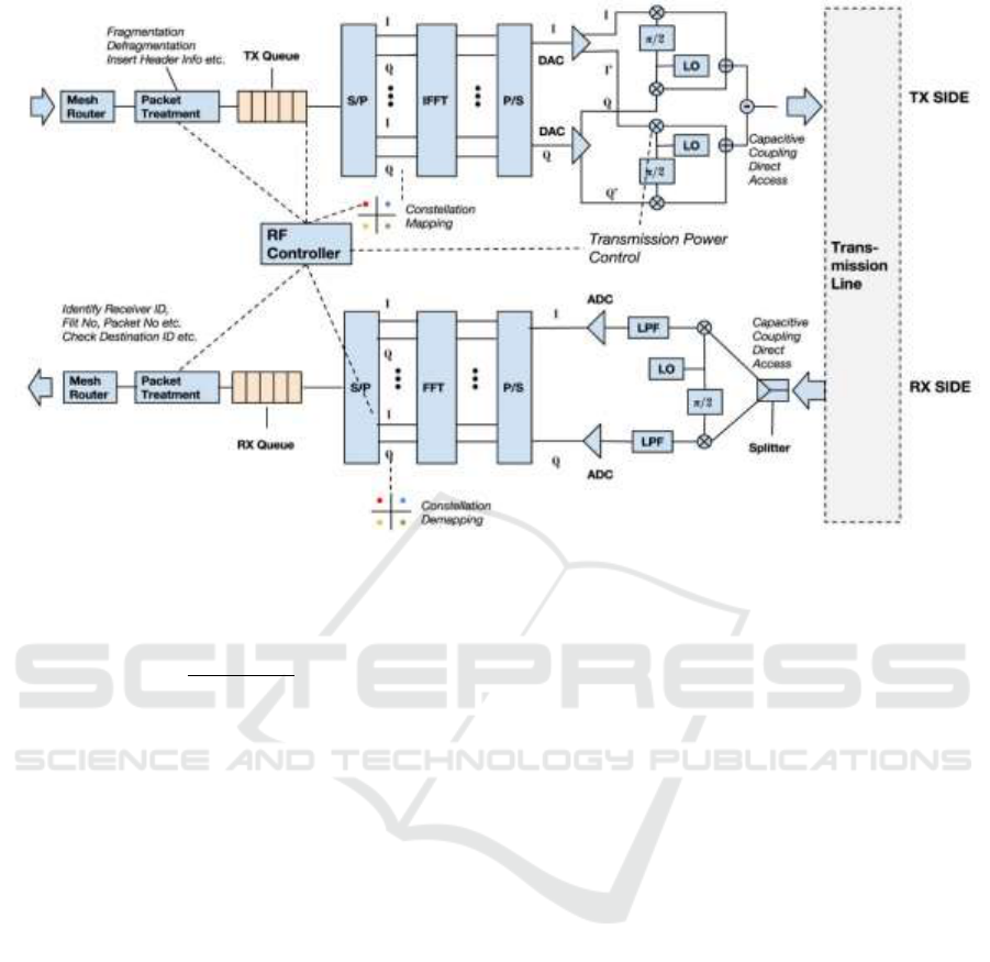
Figure 2: The detailed illustration of transmission and reception RF interface of a tileset.
0.25 /10
10
T
R
dij
P
P
(2)
Spectral efficiency in bits/sec/Hz, SE = C
0
/ B, is
a metric that we use more frequently, which defines
the achievable transmission rate per bandwidth. By
inverting the capacity formula, one can also derive the
required minimum transmission power (linear), P
T
as
a function of desired spectral efficiency, SE:
0.25 /10
10 2 1
ij
d
SE
TN
PP
(3)
This calculated minimum transmission power
shall provide a good rationale for users on the
requirements of error-free reliable communication.
In this paper, we will analyze the information
theoretic channel capacities and associated minimum
transmission power values for our RF based on-chip
interconnect. In addition to this, required
transmission powers for different bit error rates for
different modulation orders and uncoded
communications are evaluated. These two type of
indicators can be compared to dimension the required
communication energy for the proposed on-chip RF
interconnect. Adjacent tileset access points have a
displacement of 8 mm and we assume that vis-a-vis
tilesets’ access points have a displacement of 1 mm.
We also assume that each tileset is allocated evenly
32 subcarriers for transmission, which corresponds to
640 MHz of bandwidth. Hence, the noise power for
the bandwidth can be calculated by multiplying it
with the assumed AWGN power spectral density and
can be found as approximately -86 dBm. Note that
one can derive desired figures for different
bandwidths simply by scaling linearly. Information
spectral capacity densities can be regarded as good
indicators for the utilizable modulation orders with
error free communication, such as 1 bits/s/Hz
corresponding to BPSK, 2 bits/s/Hz corresponding to
QPSK etc.
However, we also investigate the required
transmission powers for various bit error rates for
different modulation orders under uncoded
transmission. Note that, information theoretic
capacity defines the maximum achievable rate with a
bit error rate approaching to 0, with a hypothesized
perfect channel coding mechanism. Therefore, even
though required transmission power for a desired
channel capacity density is defined for an error rate of
0, it may require less power than the power required
for various bit error rates. This is due to robustness of
channel coding. Next, we develop the expressions for
the required transmission powers for different
modulation orders. For BPSK and QPSK, the BER or
Fifth International Conference on Telecommunications and Remote Sensing
74

probability of bit error (p
b
) can be written as
(Goldsmith, 2005):
2
bb
p Q SNR
(4)
where Q(.) is the Gaussian tail function and SN R
b
is
the received SNR per bit. For square M-QAM
constellation symbols (such as 16-QAM, 64-QAM ..),
p
b
can be written approximately as (Goldsmith,
2005):
3
21
b
b
b
SNR b
pQ
(5)
where b is the number of bits per constellation such
as 4 bits for 16-QAM, 8 bits for 256-QAM etc. Let us
calculate the SNR per bit at first. As we did in
capacity formula in (2), we can write the received
SNR as the ratio of transmission power to ambient
noise power and attenuation by distance. For BPSK
and QPSK. By using the assumption made in
(Hamieh et al., 2014), a noise factor, F of 3 dB is used,
which is approximately 2 in linear scale. Therefore,
the linear noise power density can be calculated from
the -174 dBm and the additional 3 dB noise factor as:
174 3 /10
21
810 10
(6)
By using this, we can calculate the BER values for
BPSK:
0.025 21
2
10 810
T
b
d
P
pQ
B
(7)
and for M-QAM:
0.025 21
3
4
10 810 2 1
T
b
db
bP
pQ
b
B
(8)
By inverting these equations we can calculate the
required minimum transmission powers with a given
BER. The minimum required transmission power for
BPSK and QPSK:
2
0.025 21 1
0.510 810
d
Tb
P B Q p
(9)
and minimum required transmission power for M-
QAM constellations:
0.025 21
2
1
1
10 810 .
3
0.25 2 1
d
T
b
b
PB
Q p b
(10)
Figure 3: Placement of tilesets with their ID number on the
U-shaped transmission line.
The placement of tilesets with their ID number is
shown on Fig. 3. For instance, one of the maximum
distances among tileset connection is between tileset-
1 and tileset-32, which is 120 mm (spacings of 15
adjacent tilesets). We have analyzed the information
theoretic limits for each of the 32x31 unicast
communication combination between tilesets. Fig. 4
shows the distances between tilesets for each of these
combinations according to tileset ID numbers.
The capacity of the each transmission
combination can be written in matrix format
assuming transmission power P
T
is allocated for each
them, where d
ij
is the distance between tileset-i and
tileset-j in mm:
12
0
2
174 3 30 10log 0.25 /10
log 1
10
ij
T
Bd
C
P
B
(11)
3.2 Results
Combining (2) and (3), we derive the required
minimum transmission powers in dBm for different
spectral capacity densities from 1 bits/s/Hz to 6
bits/s/Hz corresponding to modulation orders
between BPSK and 64-QAM. One can see that from
Fig.5, for achieving a spectral efficiency of 1
bits/s/Hz between the most distant tilesets, we need
approximately - 40 dBm transmission power and
between the closest tilesets, we need approximately -
70 dBm transmission power. For achieving a spectral
efficiency of 6 bits/s/Hz between the most distant
tilesets, we need approximately -20 dBm transmission
power and between the closest tilesets, we need
approximately -50 dBm transmission power. Note
that, the transmission power in dBm varies linearly
with spectral efficiency and distances between
tilesets, consistent with the equations above.
Capacity Analysis of Radio Frequency Interconnect for
Manycore Processor Chips
75
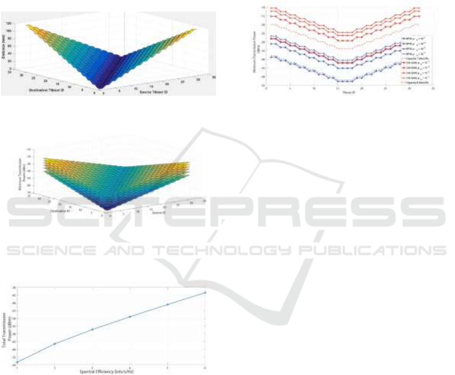
Fig. 6 shows the total required transmission
power, considering each of the unicast
communication combination has capacity densities 1-
6 bits/s/Hz. We can see that for achieving a spectral
efficiency of 1 bits/s/Hz, we need approximately - 57
dBm total transmission power and for a spectral
efficiency of 6 bits/s/Hz, we need approximately -42
dBm average transmission power.
Figure 4: Distance between each 32x31 unicast
communication pair in our U-shaped transmission line.
Figure 5: Required Transmission Power for each 32x31
unicast communication for the linear (U-shaped) shaped
transmission line for capacity densities 1-6 bits/s/Hz.
Figure 6: Total Required Transmission Power of 32x31
unicast communication for the U-shaped shaped
transmission line for capacity densities 1-6 bits/s/Hz.
And finally, Fig.7 shows the minimum required
overall transmission power from each tileset to their
31 destinations, for bit error rates of 10
-1
; 10
-3
; 10
-5
and 10
-7
for the lowest and highest modulation orders;
BPSK and 64-QAM. As a reference, overall required
transmission powers for information theoretic
capacity densities of 1 bits/s/Hz and 6 bits/s/Hz
(which are associated to BPSK and 64-QAM
respectively) are shown. Note that, minimum
required overall power for bit error rates of 10
-3
; 10
-5
;
10
-7
for BPSK and 64-QAM are higher than the power
required for information theoretic capacity densities
of 1 bits/s/Hz and 6 bits/s/Hz, respectively. This is due
to capacity’s definition for perfect channel coding as
mentioned previously.
Figure 7: Average required transmission power from each
tileset to their 31 destinations, for bit error rates of: 10
-1
;
10
-3
; 10
-5
; 10
-7
under BPSK and 64-QAM and information
theoretic capacity densities of 1 bits/s/Hz and 6 bits/s/Hz.
4 CONCLUSIONS
We have briefly presented the architecture of a 2048-
core generic multiprocessor, which is being
developed in the scope of WiNoCoD project, which
attempts to employ an OFDMA based on-chip RF
interconnect for the first time, to the best of our
knowledge. With their matured manufacturing
techniques, full CMOS compatibility and ever
increasing transistor frequencies, RF interconnects
are considered viable candidates of future massive
on-chip platforms. We have given details of this 20
GHz OFDMA infrastructure to be used by 32 tilesets,
where each of them incorporates 64 cores.
Information theory defines the limits for the
achievable transmission rate with given power budget
and noise characteristics. Information theoretic
capacities and the associated minimum transmission
powers for this interconnect have been evaluated in
this paper.
ACKNOWLEDGEMENTS
This work is supported by French National Research
Agency (ANR) under No. ANR-GUI-AAP-05. The
authors would also like to thank to LIP6, ETIS,
ENSEA laboratories and NXP Semiconductors.
Fifth International Conference on Telecommunications and Remote Sensing
76

REFERENCES
Borkar, S., “Thousand core chips: a technology
perspective,” in Proceedings of the 44th annual Design
Automation Conference. ACM, 2007, pp. 746–749.
Olukotun, L., K. Hammond, and J. Laudon, “Chip
multiprocessor architecture: techniques to improve
throughput and latency,” Synthesis Lectures on
Computer Architecture, vol. 2, no. 1, pp. 1–145, 2007.
Cota, E., A. de Morais Amory, and M. S. Lubaszewski,
Reliability, Availability and Serviceability of
Networks-on-chip. Springer, 2011.
Pasricha S., and N. Dutt, On-chip communication
architectures: system on chip interconnect. Morgan
Kaufmann, 2010.
Deb, S., “Millimeter-wave wireless network-on-chip: A
cmos compatible interconnection infrastructure for
future many-core processors,” Ph.D. dissertation,
Washington State University, 2012.
Bri`ere, A., J. Denoulet, A. Pinna, B. Granado, F. Pˆecheux,
E. Unlu, Y. Lou¨et, and C. Moy, “A dynamically
reconfigurable rf noc for manycore,” in Proceedings of
the 25th edition on Great Lakes Symposium on VLSI.
ACM, 2015, pp. 139–144.
Lilja, D. J. “Cache coherence in large-scale shared-memory
multiprocessors: issues and comparisons,” ACM
Computing Surveys (CSUR).
Kurian, G., J. E. Miller, J. Psota, J. Eastep, J. Liu, J. Michel,
L. C. Kimerling, and A. Agarwal, “Atac: a 1000-core
cache-coherent processor with on-chip optical
network,” in Proceedings of the 19th international
conference on Parallel architectures and compilation
techniques. ACM, 2010, pp. 477–488.
Hamieh, M., M. Ariaudo, S. Quintanel, and Y. Lou¨et,
“Sizing of the physical layer of a rf intra-chip
communications,” in Electronics, Circuits and Systems
(ICECS), 2014 21st IEEE International Conference on.
IEEE, 2014, pp. 163–166.
Shannon, C. E. “A mathematical theory of
communication,” ACM SIGMOBILE Mobile
Computing and Communications Review, vol. 5, no. 1,
pp. 3–55, 2001.
Shankar, P. M. Introduction to wireless systems. Wiley
New York, 2002.
Goldsmith, A. Wireless communications. Cambridge
university press, 2005.
Capacity Analysis of Radio Frequency Interconnect for
Manycore Processor Chips
77
