
DOUBLE PRECISION SPARSE MATRIX VECTOR
MULTIPLICATION ACCELERATOR ON FPGA
Sumedh Attarde, Siddharth Joshi, Yash Deshpande
Electrical Engineering Department, Indian Institute of Technology Bombay, Bombay, India
Sunil Puranik
Computational Research Laboratories, Pune, India
Sachin Patkar
Electrical Engineering Department, Indian Institute of Technology Bombay, Bombay, India
Keywords:
Sparse matrix vector multiplication, FPGA, Embedded scientific computing, DRAM.
Abstract:
In this paper, we present the design of an embedded system performing double precision sparse matrix vec-
tor multiplication (SpMxV), a key scientific computation kernel in iterative solvers, for very large matri-
ces (millions of rows). The embedded system is implemented using the Xilinx MicroBlaze platform on the
XUPV5-LX110T FPGA development board. Due to their size, matrices generally encountered in scientific
computation need to be stored on off-chip DRAMs. A novel processing paradigm involving blocking of the
matrix, and a novel data access mechanism which pre-fetches required data in bursts from off-chip DRAMS
to hide large DRAM random access latencies are proposed and implemented. The processing element has
been implemented as a prototype accelerator peripheral in an embedded system for the iterative Gauss-Jacobi
algorithm.
1 INTRODUCTION
Modern embedded computing devices call for in-
creasingly complex functionality. Commercial hand-
held devices (smartphones) need to perform heavy
image processing, image reconstruction tasks. Engi-
neering applications like seismic imaging, oil explo-
ration require enormous amounts of scientific com-
puting to be done in a short time on-site. Tradi-
tionally, an enormous amount of computing power
is used for such scientific computation, which is dif-
ficult to be deplyed in a hand-held device. Such
applications would benefit from compact embedded
solutions which could be deployed in such scenar-
ios. Developing low-power embedded systems capa-
ble of handling large scientific computations certainly
seems to be a step in this direction when the world is
moving towards energy efficient alternatives.
Sparse Matrix Vector Multiplication (SpMxV) is a
key computational kernel in many scientific and engi-
neering applications. Least square problems, eigen-
value problems, FEM, computational fluid dynam-
ics, image reconstruction in medical imaging, oil
exploration, seismic imaging, circuit analysis, web-
connectivity and many more applications need to
solve sparse linear systems using iterative methods.
These problems generally involvevery large matrices,
of the order of tens of millions of non-zero elements.
Embedded systems impose constraints pertaining
to area, power and response time. The memory sub-
system is affected by all these components. For the
application at hand, large amounts of memory are the
primary requirement. Thus in order to achieve high
memory density, DRAMs (Dynamic RAMs) offer the
most viable solution. Large matrices which have sizes
running into millions of rows cannot fit in the caches
of general purpose processors. Since memory ac-
cesses are irregular, cache hierarchy loses its effec-
tiveness and many random accesses to high latency
DRAMs are made. This causes performance of Sp-
MxV to drop to a fraction of peak performance for
general purpose processors. It is only by optimiza-
476
Attarde S., Joshi S., Deshpande Y., Puranik S. and Patkar S..
DOUBLE PRECISION SPARSE MATRIX VECTOR MULTIPLICATION ACCELERATOR ON FPGA.
DOI: 10.5220/0003400804760484
In Proceedings of the 1st International Conference on Pervasive and Embedded Computing and Communication Systems (PECCS-2011), pages
476-484
ISBN: 978-989-8425-48-5
Copyright
c
2011 SCITEPRESS (Science and Technology Publications, Lda.)

tion and tuning of SpMxV kernels for the specific
matrix structures that these shortcomings can be over-
come(Williams et al., 2007).
Modern FPGAs provide abundant resources for
floating point computations. Aside from large logic
capabilities, these FPGAs also have sufficient on-chip
single-cycle access blocks of RAM (BRAMs) to pro-
vide required on-chip memory bandwidth. On the
other hand, a large number of I/O pins are available
to provide high memory bandwidth in case external
off-chip memories are to be used. However, off-chip
memories like DRAMs have large access latencies
and can considerably slow down the system if used
naively.
We present the design of a prototype embedded
system geared to accelerate SpMxV for scientific
computing. Since such an embedded system relies on
high random access latency DRAMs, data is stored
in a fashion amenable to burst accesses, thus hiding
DRAM access latencies. The Xilinx MicroBlaze plat-
form was chosen as platform for the embeddedsystem
and implemented on the Xilinx XUPV5-LX110T de-
velopment board.
2 PROBLEM DESCRIPTION
SpMxV requires that two elements - a non-zero ele-
ment from the matrix and an element from the vec-
tor - be fetched and multiplied. The result is accu-
mulated into the appropriate result vector element.
Thus two operations - a multiply and an accumulate
- are performed for every pair of the two elements.
These elements are not required for further process-
ing and are thus discarded. Only the result of the
multiply-accumulate operation is stored. Since two
input words are useful for only two computation oper-
ations, the ratio of computation to bandwidth require-
ment is low compared to other applications (namely
general matrix-matrix multiplication). This ratio be-
comes worse due to overhead of bandwidth require-
ment for fetching pointers - two per matrix element.
Assuming 32-bit pointers and double precision float-
ing point matrix and vector data, 24 bytes are fetched
in order to perform 2 floating point operations. Hence,
the performanceof SpMxV is usually less than a tenth
of the bandwidth available to the system.
Though modern FPGAs have large amounts of
fast access memories, they still fall short of the
amount of storage required in case the matrix and/or
vector data is to be stored in on-chip memories. The
largest Virtex-5 device has less than 24 Mb of storage
and devices in the the latest Virtex-6 family too has
less than 48 Mb of on-chip memory. Assuming 64-bit
data, this translates to 0.4M words and 0.8M words
in case of Virtex-5 and Virtex-6 devices respectively.
Moreover, as discussed in the above paragraph, if vec-
tor elements need to be replicated, then the size of the
matrices that can be handled drops far short of the
one million rank. Hence, an implementation geared
to handle matrices having multi-million rows has to
use external DRAMs for storage.
2.1 Related Work
We shall be referring to the work done by Prasanna
(Zhuo and Prasanna, 2005), Gregg (Gregg et al.,
2007), deLorimier (deLorimier and DeHon, 2005),
Sun (Sun et al., 2007) and Kuzmanov (Kuzmanov and
Taouil, 2009). The first three implementations aim
to accelerate iterative solvers via SpMxV on FPGAs.
With the exception of the architecture developed by
Gregg, DRAMs have not been used as the main stor-
age for matrix and vector data.
The SpMxV kernel implemented in a multi-FPGA
architecture by Zhuo and Prasanna was among the
earliest in the field. They use Compressed Row Stor-
age (CRS) format for their input which trims the ze-
ros from the sparse matrix rows. In their architecture,
each trimmed row is divided into sub-rows of fixed
length equal to the number of processing elements.
The dot products in a sub-row are assigned to differ-
ent processing elements and then a reduction circuit is
used to get the final vector element after all sub-rows
have been processed. This updated value is stored in a
second FPGA, and communication costs are reduced
for conjugate-gradient (CG) routine across iterations.
Optimizations to their design include load balancing
by merging appropriate sub-rows and padding them
with zeros if necessary, which significantly improves
performance. However the architecture proposed by
them relies on SRAMs for storage of matrix entries
which severely limits the matrix size. Large num-
ber of parallel accesses to the SRAMs contributes to
a bottleneck in the design. Moreover the entire vec-
tor is replicated in local storage of all processing ele-
ments. The sequential nature of the inputs to the al-
ready huge reduction circuit results in very high la-
tencies. The largest matrix evaluated had 21200 rows
and 1.5 million non-zeros. They reported an average
performance of 350 MFLOPS on a Virtex-II Pro de-
vice.
Special care has been taken by Gregg et. al to cre-
ate a DRAM based solution. They use pre-existing
SPAR architecture originally developed for ASIC im-
plementation and hence port a deeply pipelined de-
sign for FPGA implementation. They use local
BRAMs to create a cache for the DRAM data since
DOUBLE PRECISION SPARSE MATRIX VECTOR MULTIPLICATION ACCELERATOR ON FPGA
477

they consider elimination of cache misses to be of
paramount importance. They reported performance
of 128 MFLOPS for three parallel SPAR computation
units. In case caching is perfect, they achieve perfor-
mance of 570 MFLOPS for three SPAR units.
The architecture developed by deLorimier uses lo-
cal FPGA Block RAMs (BRAMs) exclusively to store
matrix as well as vector data. While pre-processing
the matrix, they exploit the statically available infor-
mation to schedule computation and communication
periods statically. The relevant micro-codeis stored in
the local storage of each processing element. To max-
imize operating frequency, the accumulator used has
a deep pipeline which could potentially cause RAW
(read after write) hazards due to the inherent feedback
in the accumulator data-path. During pre-processing,
they re-order the matrix and interleave rows to pre-
vent RAW hazards thus circumventing the need for
expensive pipeline stalls which might have had to be
enforced. However, the architecture has an enforced
communication stage which is not overlapped with
computation stage, decreasing the overall efficiency
of the system. The main limitation of the system is
its inability to handle designs larger than what the
BRAMs can accommodate. The largest matrix evalu-
ated had 90449 rows and 1.8 million non-zeros. They
reported performance of 1.6 GFLOPS for 1 Virtex-II
6000 and about 750 MFLOPS per FPGA with 16 FP-
GAs.
The architecture implemented by Kuzmanov
(Kuzmanov and Taouil, 2009), is capable of being dy-
namically configured to perform sparse matrix-vector
multiplication or dense matrix-vector multiplication
based on the sparsity of the matrix. The design is im-
plemented on an Altix 450 machine with SGI RASC
services, which couples dual-core Itanium processors
with Xilinx Virtex-4 devices. The SGI RASC core
contains 5 SRAM banks with a combined capacity of
a few hundred MBs of storage. This would severely
limit the size of matrices which can be handled, un-
less there is a provision for feeding data to the SRAM
banks from the host machine. The time required for
these transfers would have to be factored in the per-
formance. Scaling the computational cores upwards
would increase these communication costs. How-
ever, the design achieves a remarkable 99% of the
peak (1600 MFLOPS) for certain matrices. The de-
sign uses double-buffering technique for storing vec-
tor, matrix (CRS format) and partial sum elements in
local on-chip FPGA fabric memories. The design also
interleavesdot productcomputations of differentrows
to prevent RAW hazards in the accumulator pipeline.
However, the rows are not distributed amongst dif-
ferent processors, which might not result in optimal
workload distribution.
The architecture implemented by Sun (Sun et al.,
2007) is aimed for implementation on Virtex-II Pro
device as an accelerator on host machines like Cray
XD-1. The design can be configured to have dif-
ferent data widths for input and output, for integer
data. This would increase bandwidth utilization. The
system used for estimating performance, uses QDR
RAM (SRAM) of size of the order of few MBs (16
MB). However, using SRAMs for storage, the design
is able to achieve more than 95% of peak performance
on most matrices at operating frequency of the order
of 175 MHz.
GPUs (Bell and Garland, 2008) do present a
performance benefit, but at the cost of high power
consumption. For the unstructured matrices arising
in economics, circuit simulation, GPUs give perfor-
mance of 2-4GFLOPS for double precision data.
3 OVERVIEW
Since SpMxV for large matrices cannot be handled
exclusively using on-chip memories, we propose a
hybrid system wherein the matrix and vector are
stored in external off-chip commodity DRAMs and
the data is cached in local on-chip memories. Since
burst accesses can help to hide DRAM latencies,
the following sections explain a processing paradigm
which enables data to be stored in a fashion amenable
to burst accesses.
Practically encountered matrices are not patholog-
ically sparse nor are they perfectly clustered, both
properties are present in them to varying degrees. We
propose that matrices be split accordingly. Clustered
non-zeros are handled by one kernel, and the outliers
by a differentone. In this paper we design an architec-
ture best suited to process the clustered blocks of non-
zeros. Since the outliers are few in number and ran-
domly arranged, they should be handled separately.
A point to note is that, the proposed design does not
aim to accelerate computation for any specific matrix
structure.
3.1 Matrix Blocking
The operationinvolving sparse matrix vector multipli-
cation is distributed amongst multiple processing ele-
ments. Since maximum throughput will be obtained
when all the processing elements are operating in par-
allel, the vector access should be as fast and conflict-
free as possible for each processing element.
The local (single-cycle access) BRAM storage in
FPGAs is not sufficient to store multiple instances of
PECCS 2011 - International Conference on Pervasive and Embedded Computing and Communication Systems
478
a multi-million double precision vector. To tackle
this problem the dense matrix is divided into square
‘dense’ blocks of certain predetermined size. A ma-
trix block size of 128×128 is small enough to allow
for multiple on-chip caches and also contains suffi-
cient non-zero elements. The block size could be
changed with no fundamental changes to the rest of
the design. Since we are using external DRAMs for
matrix and data storage, we aim to make maximum
use of the burst accesses of DRAM to hide the access
latencies. As described in previous paragraph, since
matrix elements are stored in the order in which they
are to be processed, matrix data can be fetched in con-
tinuous stream of bursts.
Only the ‘dense’ blocks are given as input to the
processing elements in a row-major fashion. A row-
strip is defined to be the set of all the blocks (128n row
aligned) having the same set of rows. A direct fall-
out of such a mechanism is that the vector too can be
blocked and thus only elements in required blocks of
the vector can be fetched using burst accesses rather
than the whole vector being stored. Moreover, we
pre-fetch the next required vector block to reduce
stalls in computation, which is instrumental in hid-
ing the DRAM access latencies. Since the blocking
is very fine, the vector block size is small and thus
the vector entries can easily be replicated in the local
storage of all processing elements, bypassing prob-
lems which may arise due to memory contention.
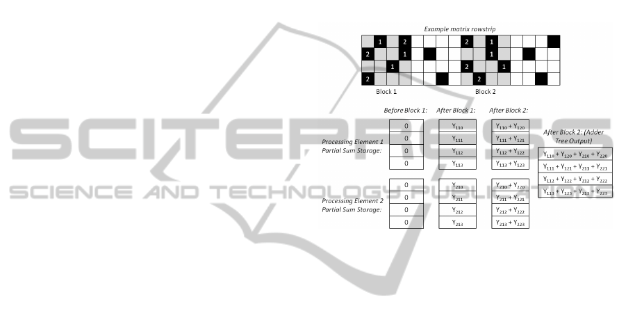
3.2 Dataflow
The matrix data is arranged in blocked column-row-
data format in the DRAM attached to each process-
ing element. During operation, ‘dense’ matrix blocks
are processed in a row major fashion one after the
other by streaming the complete matrix word from
DRAM into the processing element. The matrix data
in each block is distributed amongst different process-
ing elements in the pre-processing phase. All pro-
cessing elements operate on the same block at any
given time. For each ‘dense’ matrix block, the pro-
cessing elements compute the product of each matrix
element assigned to it and the appropriate vector el-
ement using the vector block replicated in each pro-
cessing element. Each processing element also main-
tains a 128 element (one for each row in block) partial
sum array, which is re-initialized to zeros at the start
of processing of a rowstrip. In each processing ele-
ment, the generated product is accumulated into that
element of these partial sum arrays corresponding to
the row of the matrix data. These partial sum arrays
are transferred out of each processing element at end
of processing of a rowstrip, after which they are ac-
cumulated in a adder tree. Thus, for each row in the
rowstrip, we get the accumulated sum which is the
corresponding row element in the result vector. This
operation is described in a scaled down example, hav-
ing two processing elements, in figure 1. In the figure,
the variable Y
ijk
represents that it is a element con-
tributing to the result vector generated by processing
element i, for row k of block j of the matrix. The
grayed blocks represent ‘dense’ blocks and numbers
represent the processing element the matrix element
is assigned to.
Figure 1: SpMxV operation.
4 DESIGN
A block diagram of the processing element is shown
in figure 2. Modules in the figure are explained in the
following section.
4.1 Vector Cache
The vector blocks which are fetched from the DRAMs
in burst accesses are replicated in the local vector stor-
age of each processing element. FPGAs have single-
cycle Block RAMs (BRAMs) which are used for im-
plementing these memories. Since the matrix is di-
vided into block sizes of 128, we need storage for
128 elements of the block currently being processed
as well as the 128 pre-fetched vector elements corre-
sponding to the next matrix block. By using simple
dual port memories, while vector elements are being
read from one half of the storage by the processing
elements, vector elements corresponding to the next
block are pre-fetched in the other half. Thus we effec-
tively utilize double-buffering technique to hide ac-
cess latencies.
Input vector blocks are stored in order which en-
sures that the result vector needs minimal manipula-
tion. This scenario has advantage of result storage
DOUBLE PRECISION SPARSE MATRIX VECTOR MULTIPLICATION ACCELERATOR ON FPGA
479
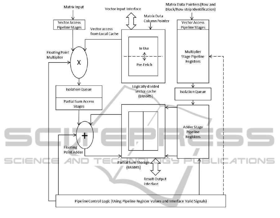
Figure 2: Block Diagram of processing element.
and the disadvantage of random input access. How-
ever, the knowledge of the sequence of access of vec-
tor blocks is static and can be provided to the vec-
tor fetching units at initialization time, reducing the
penalty for random block access making the second
scenario more feasible than the first for iterative ap-
plications. Moreover within a block, the vector data
elements are sequentially stored, which ensures that
data can still be accesses in burst.
4.2 Floating Point Multiplier
A fully IEEE-754 compliant double precision floating
point multiplier, generated using Xilinx CoreGenera-
tor was used in the design. The multiplier (Coregen
IP v4.0) is deeply pipelined for high throughput, is
10-stage pipelined and requires 13 DSP48E slices.
4.3 Floating Point Adder
A fully IEEE-754 compliant double precision float-
ing point adder, generated using Xilinx CoreGenera-
tor was used in the design. The adder is pipelined for
high throughput. However, since the adder functions
as an accumulator, there is a loop from adder output
to adder input through local partial sum memory. This
has the potential to cause RAW hazards, since the
adder might try to read from an address whose valueis
still in the pipeline and this not been updated. Hence
we would not want the pipeline to be very deep, as
this would compromise on the efficiency of operation
and offset the advantage offered by deeper pipelining.
The adder (Coregen IP v4.0) is 14-stage pipelined and
requires 3 DSP48E slices.
4.4 Partial Sum Storage
Since we process the matrix in blocks of 128×128,
we need storage for 128 partial sums in each process-
ing element, each corresponding to one of the 128
rows in the block being processed. When processing
for a row strip is done, the partial sums correspond-
ing to that row strip need to be transferred out of the
processing element. This would take as many clock
cycles as the depth of the partial sum storage. If we
have only one buffer for storing partial sums, the en-
PECCS 2011 - International Conference on Pervasive and Embedded Computing and Communication Systems
480
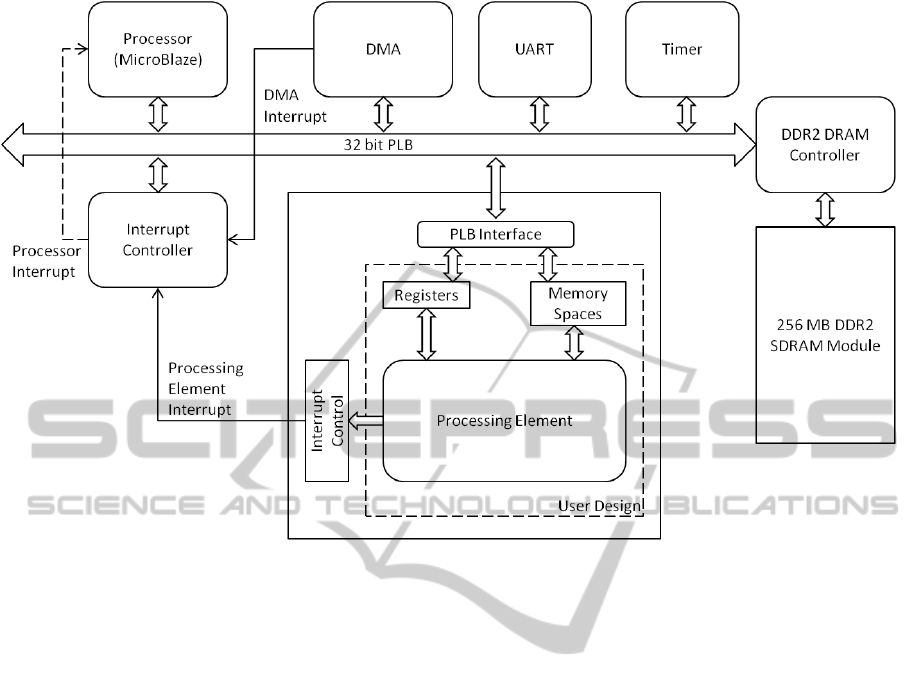
Figure 3: Embedded System Schematic.
tire processing pipeline will have to halt while this
transfer is in progress. To prevent such situations, as
in the case of the vector storage, we have a double-
buffered memory system for storing the partial sums
generated by each processing element. This ensures
that the accumulator does not have to stall while the
partial sums are being read out of the processing ele-
ment at the end of a row strip. Since each processing
element can potentially generate 128 partial sums, the
size of the storage buffer is enlarged to 256 elements.
While the accumulator reads as well as writes to
one of the ping-pong memory buffers in the storage,
the other buffer is simultaneously being emptied and
initialized to zero. Thus during certain periods of op-
eration more than two ports are needed. A simple
dual-port memory, as used for vector storage or even
a true dual-port memory provides only two ports. As
a result, we need two simple dual port memories serv-
ing as separate storage buffers, each of 128 elements
as opposed to one big buffer of 256 elements.
4.4.1 Pipeline and Control
We have two pipelines separated by an isolation
queue. The first pipeline comprises of vector access
stage (4 stages), multiplier stage (10 stages) and the
second comprises of the partial sum access stage (2
stages) and adder stage (14 stages). The pipeline
serves as a delay mechanism (using shift registers)
for the address pointers so that they are available at
the right time in different stages of the computation
pipeline. This unit also contains pipeline stall control
logic.
5 SYSTEM IMPLEMENTATION
As a proof of concept, we implemented the process-
ing element as a prototype accelerator peripheral in
an embedded system. The Gauss-Jacobi iterative al-
gorithm (Golub and Loan, 1996) is the application
chosen for acceleration using the sparse matrix vector
multiplication processing element described in sec-
tion 4. Typically, in most iterative methods, and
Gauss-Jacobi is no exception, operations other than
sparse matrix vector multiplication have structured
accesses. These operations can be efficiently per-
formed by a simple off-the-shelf micro-processor in
conjunction with a cache. In the following sections,
the embedded system comprising of a soft proces-
sor and peripheral units such as DDR2 DRAM con-
troller, DMA controller, interrupt controller and bus
controller is described.
5.1 System Description
The embedded system is developed around the 32-bit
DOUBLE PRECISION SPARSE MATRIX VECTOR MULTIPLICATION ACCELERATOR ON FPGA
481

MicroBlaze processor, a soft processor provided by
Xilinx along with the proprietary embedded develop-
ment kit. The processor is configured to operate at
125 MHz and have 64KB data cache. The board used
for prototyping, Xilinx XUPV5-LX110T also incor-
porates a 256 MB DDR2 SDRAM module which pro-
vides the system with the capability to handle large
matrices.
A DMA controller is included to facilitate burst
transfers of data from DRAMs to processing element.
The DMA can be configured to have variable inter-
nal storage, and variable read and write burst sizes.
To hide DRAM latencies, DMA is configured to have
read and write burst size of 16 which is the maximum
supported by the peripheral.
The system has the processing element as well as
the DMA for interrupt sources. Since the processor
has only one interrupt line, an interrupt controller is
included to enable processor to respond to interrupt
requests as well as prioritize the requests. The pro-
cessing element generates three types of interrupts -
request storage of result vector block, request input
vector block and request matrix data. The DMA gen-
erates an interrupt to indicate transfer completion.
The peripherals are connected to the processor us-
ing PLB (Peripheral Local Bus) which has a width of
32, operates at 125 MHz and can support burst trans-
fers. A seperate link - Xilinx Cache Link - between
the processor and the DDR2 DRAM memory con-
troller is also included to support caching of DRAM
data.
Figure 3 shows a schematic of the embedded sys-
tem.
5.2 Hardware and Software
Development
Each of the three interfaces - matrix, vector and partial
sum transfer interfaces - generates an interrupt sig-
nal requesting transfer of data and then communicates
with the software till the end of the transaction. In this
section, control flow in both hardware and software is
explained side by side.
The hardware state machines controlling the inter-
faces, after generating the interrupt, wait for acknowl-
edge, then mask the interrupt signal and wait for
the transfer complete notification after which they go
back to their initial state. Interrupt acknowledge and
DMA transfer are multi-cycle processes and thus the
hardware state machines have no information about
their progress. They will keep on interrupting the pro-
cessor even after interrupt has been acknowledged,
if there is no communication between software and
hardware.
Hence for each interface, the software controls a
pair of signals - interrupt acknowledge and transfer
done - represented as bits in a programmervisible reg-
ister, which initially represent false condition. When
an interrupt is received, software clears the transfer
done signal and only then sets interrupt acknowledge.
This ensures that transfer done signal set high for the
previous transfer is not interpreted by the hardware
state machine for the current transfer. After the DMA
signals end of transfer, first interrupt acknowledge is
cleared and only then transfer done is set. This is es-
sential because a register write by software is a multi-
cycle process. If transfer done is set before clear-
ing interrupt acknowledge, and an interrupt request
is generated in between, the hardware state machine
would interpret the acknowledge for the most recent
interrupt.
The rest of the application software follows the
following flowchart as depicted in figure 4.
However such an embedded system has certain
limitations which are enumerated below.
1. The soft processor available is a 32-bit processor.
This decreases bus width to 32 bits, in turn de-
creasing the bandwidth available to the process-
ing element. Multiple clock cycles are required to
transfer just one matrix/vector/result word.
2. A single processor embedded system can contain
only one bus. Requests to the DRAM have to be
made on the same bus on which the DRAM pro-
vides data. Firstly, this reduces throughput since
requests cannot be queued. Secondly, this will in-
crease number of bus turnarounds.
3. The board provides only one DRAM interface
thus decreasing number of processing elements
supported and imposing need to time-multiplex
transfers.
4. The DMA controller module makes requests for
maximum burst size of 16. Such a small burst is
not sufficient to hide DRAM access latency.
5. Data is transferred from source to internal DMA
storage, and then transferred from the DMA stor-
age to the destination. Thus data needs to be trans-
ferred twice along the same bus. The time re-
quired for bus turnaround worsens the situation.
However, this problem can be alleviated by in-
cluding a bus master unit in the PLB interface.
6 CONCLUSIONS
In this paper an approach for embedded system de-
sign for sparse matrix-vector multiplication using the
PECCS 2011 - International Conference on Pervasive and Embedded Computing and Communication Systems
482
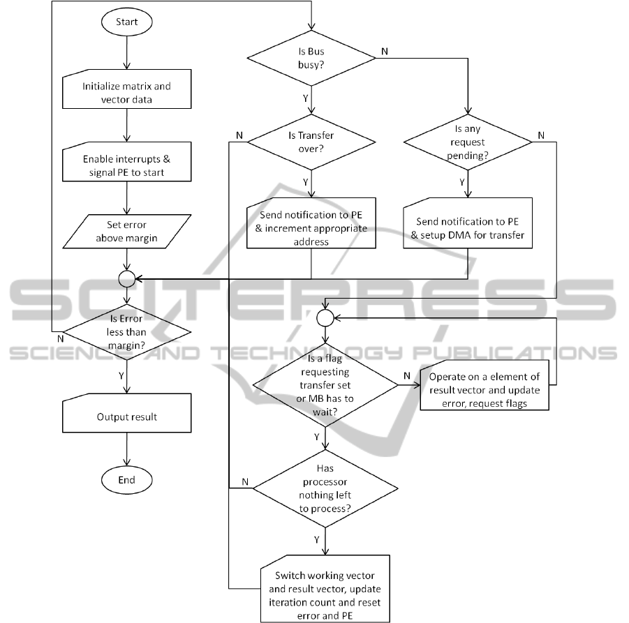
Figure 4: Software Flow.
MicroBlaze platform by Xilinx, is presented and dis-
cussed. The paper discusses the trade-offs for the Sp-
MxV architecture, it aims to provide insight into the
design of accelerators. The simplicity of the design
and the use of commodity DRAMs makes this design
a practical accelerator.
REFERENCES
Bell, N. and Garland, M. (2008). Efficient sparse matrix-
vector multiplication on CUDA. NVIDIA Technical
Report NVR-2008-004, NVIDIA Corporation.
Davis, T. and Yu, H. (2010). The university of florida sparse
matrix collection. http://www.cise.ufl.edu/research/
sparse/matrices/.
deLorimier, M. and DeHon, A. (2005). Floating-point
sparse matrix-vector multiplication for fpgas. FPGA
2005: Proceedings of the 2005 ACM/SIGDA 13th in-
ternational symposium on Field-programmable gate
arrays, pages 75–85.
Golub, G. H. and Loan, C. F. V. (1996). Matrix Computa-
tions. Johns Hopkins University Press, 3 edition.
Gregg, D., McSweeney, C., McElroy, C., Connor, F.,
DOUBLE PRECISION SPARSE MATRIX VECTOR MULTIPLICATION ACCELERATOR ON FPGA
483

McGettrick, S., Moloney, D., and Geraghty, D.
(2007). Fpga based sparse matrix vector multipli-
cation using commodity dram memory. FPL, pages
786–791.
Kuzmanov, G. and Taouil, M. (2009). Reconfigurable
sparse/dense matrix-vector multiplier. Proceedings of
the International Conference FPT 2009, pages 483–
488.
Morris, G. R. and Prasanna, V. (2007). Sparse matrix com-
putations on reconfigurable hardware. Computer, vol
40, no 3, pages 58–64.
Morris, G. R., Prasanna, V. K., and Anderson, R. D.
(2006). A hybrid approach for mapping conjugate gra-
dient onto an fpga-augmented reconfigurable super-
computer. FCCM ’06: Proceedings of the 14th An-
nual IEEE Symposium on Field-Programmable Cus-
tom Computing Machines, pages 3–12.
Sun, J., Peterson, G., and O.O, S. (2007). Mapping sparse
matrix-vector multiplication on fpgas. Proc. Recon-
figurable Systems Summer Inst. (RSSI).
Williams, S., Oliker, L., Vuduc, R., Shalf, J., Yelick, K., and
Demmel, J. (2007). Optimization of sparse matrix-
vector multiplication on emerging multicore plat-
forms. SC ’07: Proceedings of the 2007 ACM/IEEE
conference on Supercomputing, pages 1–12.
Zhuo, L. and Prasanna, V. (2005). Sparse matrix-vector
multiplication on fpgas. FPGA 2005: Proceedings of
the 2005 ACM/SIGDA 13th international symposium
on Field-programmable gate arrays, pages 63–74.
PECCS 2011 - International Conference on Pervasive and Embedded Computing and Communication Systems
484
