
HIGH THROUGHPUT MEMORY-EFFICIENT VLSI DESIGNS
FOR STRUCTURED LDPC DECODING
Hrishikesh Sharma, Subhasis Das, Rewati Raman Raut and Sachin Patkar
Dept. of Electrical Engineering, IIT Bombay, Bombay, India
Keywords:
Error-correction codes, LDPC decoder, VLSI design.
Abstract:
Low-density Parity Check(LDPC) codes have been in focus of intense research in Error-correction Coding
in recent years. High throughput decoder design for them has been a big challenge for these codes. In this
paper, we report the first scalable VLSI decoder design based on projective geometry (PG) structure of LDPC
codes. The design is based on memory-efficient communication primitives known as perfect access sequences.
A high-throughput variation of above design achieves a throughput of 620 Mbps, much higher than what
communication standards require. The corresponding fully-parallel VLSI architecture was implemented on
Xilinx LX110T FPGA, as well as on 90-nm SAED EDK90 CORE Cell Library from Synposys. We find that
PG-based graphs indeed offer an exciting way of parallelizing this computation, and many others in future.
1 INTRODUCTION
LDPC codes are an emerging class of codes which ex-
hibit superior bit error rate(BER) performance. Rela-
tive ease of decoder design, coupled with better per-
formance, has made LDPC codes started being used
in recent digital transmission and storage systems. All
LDPC decoding algorithms need large number of par-
allel working memories. Hence designing for mem-
ory efficiency is one of the significant problems in its
decoder design (Tarable et al., 2004). In this work,
we first report an LDPC decoder design that simply
uses a particular hardware scheduling to avoid mem-
ory bottlenecks arising from on-chip access conflicts.
In general, different code structures result in
different architectures, and hence different memory
management schemes. Our choice of structures is de-
rived out of geometry of projective planes (Kou et al.,
2001). This choice of structure can avoid memory
conflicts. We report prototype implementation results
on FPGA, to demonstrate simplicity of design, and
high efficiency of the hardware, for PG-based LDPC
codes, apart from throughput improvement. To over-
come one of the limitations of the first design, which
inhibited its throughput, a second design has also been
presented. The second design has been implemented
both for FPGA and ASIC targets.
2 OVERVIEW OF LDPC CODES
LDPC codes are generally decoded using probabilis-
tic soft decision decoding process. The knowledge
of channel noise statistics is used to generate prob-
abilistic information for received bits, and given to
the decoder. The reliability of this bit information
is then successively improved over iterations, and
hard decisions on bit values made. Such decoders
make use of graphs known as Tanner graphs to repre-
sent codes, passing probabilistic messages along the
graph’s edges iteratively. The adjacency matrix of
this graph is called parity-check matrix H. A Tan-
ner graph has two sets of nodes: n bit nodes, and m
parity-check nodes, for a m×n sized parity-check ma-
trix. Each parity-check node is connected by an edge
to bit nodes corresponding to the code bits included
in that parity-check equation. The sequence of steps
involved in iterative decoding using log-sum-product
algorithm are as follows(Johnson and Weller, 2003).
1. The initial message is first sent by bit nodes to
check nodes. This message is based on the calcu-
lated log-likelihood ratio(LLR) of received signal.
2. Next, check nodes calculate and send updated
LLRs to the bit nodes using the received mes-
sages. Computation is performed separately on
the sign and magnitude parts of these messages.
A XOR on the sign bits of the incoming bit mes-
sages forms the parity check result for the matrix
518
Sharma H., Das S., Raman Raut R. and Patkar S. (2011).
HIGH THROUGHPUT MEMORY-EFFICIENT VLSI DESIGNS FOR STRUCTURED LDPC DECODING.
In Proceedings of the 1st International Conference on Pervasive and Embedded Computing and Communication Systems, pages 518-521
DOI: 10.5220/0003366305180521
Copyright
c
SciTePress
row. The sign of each outgoing check message for
each edge of the graph is formed by further XOR-
ing the sign of the incoming bit message of that
edge with the row parity check result. The mag-
nitude of outgoing check message(extrinsic relia-
bility) is computed in the logarithmic domain as
λ
o
pr
= 2 tanh
−1
exp
ϕ
λ
i
p
− ln
tanh
λ
p
pr
2
ϕ
λ
i
p
=
∑
∀q:H
pq
=1
ln
tanh
λ
i
pq
2
where λ
o
pr
is the (output) reliability of the check
message, λ
i
pq
the input message, and ϕ(x) is de-
fined as ϕ(x) = − lntanh (|x|/2).
3. Next, syndrome test is done using combined LLR
L
p
=
∑
∀q:H
pq
=1
λ
o
pq
+ R
p
of intrinsic(R
p
) and extrinsic messages. A hard
decision of bit being 0 or 1 is then made using
the sign of L
i
. From this set of decided bits z,
if in some iteration H · z
T
= 0, then the decoded
codeword is supposed to be z
T
.
4. Else, updated messages, called residues, are sent
back to check nodes
γ
pr
=
∑
q
∈
H
i
,
q
̸
=
r
λ
o
pq
+ R
p
and the iterations continue until convergence.
In a modified algorithm used in the second design,
min-sum algorithm, calculation of λ
o
pr
in step (2) is
simplified to
λ
o
pr
= min
j,h
pq
=1,q̸=r
λ
i
pq
− 0.693
3 PARALLEL SCHEDULING
MODEL
The scheduling model used in first design is based
on Karmarkar’s template(Karmarkar, 1991). By def-
inition, a projective plane of order s contains n =
s
2
+ s + 1 points and as many lines. Each line is con-
nected to s + 1 points, and vice-versa. Given n pro-
cessing units and a memory system partitioned into
n memory blocks M
1
, M
2
, ·· · M
n
, Karmarkar’s tem-
plate can be applied by mapping memory blocks to
points and processing units to the lines. A memory
block and a processing unit are connected if the cor-
responding point belongs to the corresponding line.
Then any operation can be scheduled on each pro-
cessing unit such that load/store of operands is based
on perfect access patterns(PAP) and sequences(PAS)
as defined in (Karmarkar, 1991). A schedule for such
a collection of operations leads to several important
advantages such as no memory conflict, full utiliza-
tion of processing units and memory bandwidth etc.
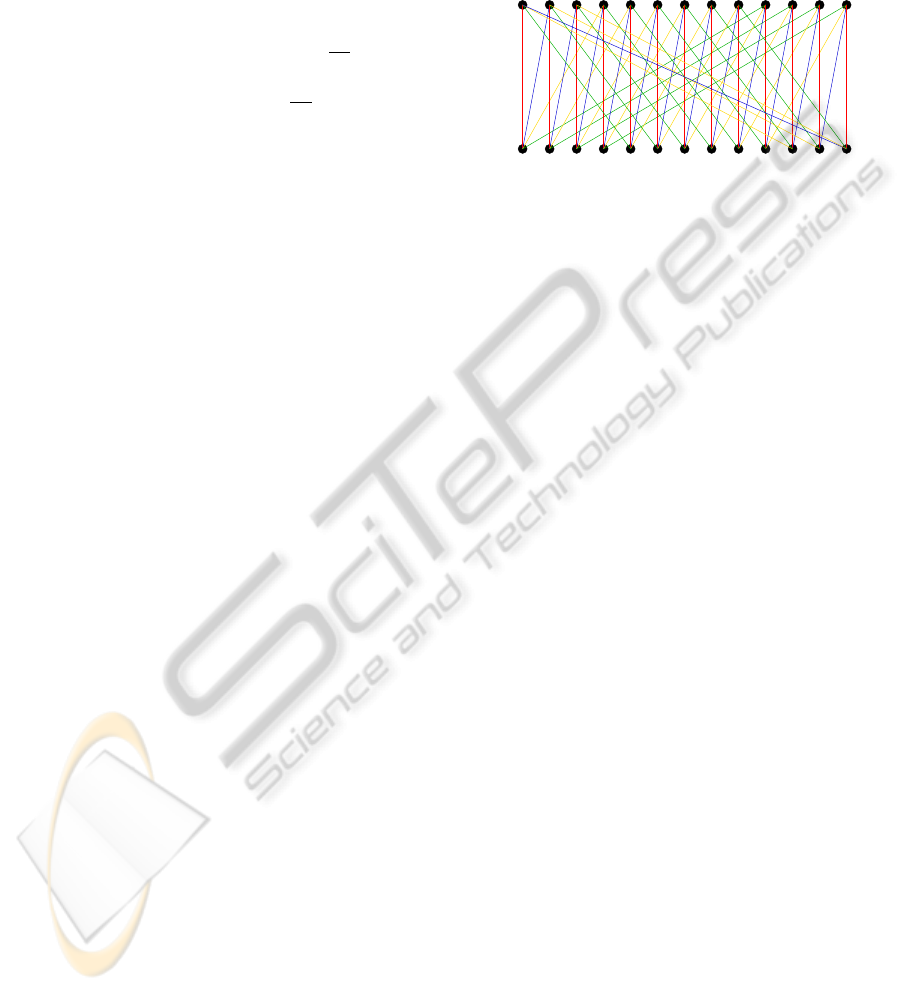
Check Nodes
Bit Nodes
Figure 1: A 2-dimensional PG as LDPC Tanner Graph.
One can argue that the behavior of regular PG-
based LDPC decoder is made up of perfect access
patterns and sequences(Sharma, 2007). Once that is
established, applicability and utility of Karmarkar’s
template is obvious. The two types of computation,
done alternately by bit and check nodes, remain same
over iterations. For each computation, the input mes-
sages have different values and hence can be stored
in (two) different sets of memory blocks. Hence we
first split the LDPC decoding iteration into two com-
putations having topology similar to that Karmarkar’s
template envisages.Thus the problem of scheduling
for PAP/PAS in LDPC decoding is decomposed into
two isomorphic scheduling problems. In each bit
node processing, majority of computation involves
adding the extrinsic information collected over all the
edges incident on the particular bit node. The num-
ber and size of input coefficients per bit node is a
constant. By taking two inputs at a time for addi-
tion, we can schedule a binary operation on each bit-
node processing unit, in every machine cycle. The
set of concurrent operations in each cycle then form
a PAP, while the set of all operations within complete
bit node processing forms the PAS. The processing is
similar in check nodes, though in log(tanh()) domain,
hence one can again find perfect access patterns in
check-node processing as well. Hence the PG-based
LDPC code decoding algorithm does exhibit behavior
which has a decomposition based on perfect access
patterns and sequences. All that remains, then, is to
deal with its refinement for detail design purposes.
4 DETAILS OF HARDWARE
MODEL
Most of the computational logic of the design is con-
tained in the node processing units. The bit nodes
HIGH THROUGHPUT MEMORY-EFFICIENT VLSI DESIGNS FOR STRUCTURED LDPC DECODING
519

read input messages from the check memories, write
back to bit memories, and vice-versa. The process-
ing units and memories are connected according to
the line/point incidences of order-8 projective plane.
For resource and speed efficiency, we chose to im-
plement the data path using 9-bit fixed-point arith-
metic, which has 1 sign, 3 integer and 5 fraction bits.
To avoid overflow during accumulation, internal data
path was made 13-bit wide in bit nodes and 12-bits
wide in check nodes. The detailed micro-architecture,
including bit-node architecture, check node architec-
ture, memory block architecture, interconnect archi-
tecture, overall data and control path design can be
found in (Sharma, 2007).
5 FPGA IMPLEMENTATION
RESULTS
The length-73 decoder implementation was targeted
to Virtex 5 LX330T FPGA. The functionality of each
bit node is mapped to CLBs, requiring 28 CLBs. Sim-
ilarly, the functionality of each check node is mapped
to 42 CLBs and 2 DSP slices, to realize the multiply-
add operations in ϕ(x) function. The bit and check
memory blocks are mapped onto BRAMs. To avoid
routing congestion on global routes, we have imple-
mented a 50% reduction in global wires by time-
multiplexing the 2 instances of PG interconnect dis-
cussed earlier. The pre-routing maximum frequency
was found to be approximately 130 MHz, which af-
ter critical path optimization, improved to 155 MHz.
The number of cycles per iteration is 42, thus the
maximum system throughput achieved at practical
SNRs(≥ 2) is ≈ 90 Mbps. This throughput matches
the requirements of WiMAX(75 Mbps) and DVB-
S2(90 Mbps). Further analysis revealed that %-wise
utilization of size of a BRAM block of LX330T was
limited. We then realized that in each cycle, the FPGA
architecture restricted the parallel memory operations
to a maximum of 2 operations per BRAM block. If
it was possible to read more datum per cycle from
each memory block, then more number of computa-
tional nodes could have been simultaneously served,
and also better utilization of each memory block size.
We then tried to do a specific high-throughput decoder
design based on distributed memory elements, rather
than block memory elements, presented next.
6 A HIGH-THROUGHPUT
MIN-SUM DECODER
Based on min-sum algorithm, we implemented a
length-73 LDPC decoder having the same parity-
check matrix, H. The internal fixed point datapath
bit-width was shrunk to 5 bits, consisting of 1 sign
bit, 3 integer bits and 1 fraction bit. The microar-
chitecture of bit and check processing units was re-
designed to account for algorithm variation. The con-
trol path was modeled as a simple 3-state simple cycle
FSM. The design was also pipelined, such that two
blocks of data are taken in at once by decoder. While
one block of data gets processed in the bit processing
units, the other block gets processed/updated in check
processing units, every iteration, simultaneously. The
processing unit’s interface was changed to allow all
the 9 inputs arrive simultaneously, since BRAMs and
two-port bottlenecks were eliminated. Also, the input
system was changed from a parallel input of all the
73 × 5 bits at one time, to a system where one bit of
each input is taken in every cycle, thus making 73 in-
put bits per cycle. This reduced the number of input
pins to a great extent and thus contributed to mini-
mizing the delays due to input buffers. The overall
microarchitecture of this design is described in (Das,
2010).
7 RESULTS AND ANALYSIS
7.1 FPGA Synthesis Results
The decoder was put on board for Xilinx Virtex-5
LX110T FPGA, and tested in similar conditions as
previous design. The maximum clock frequency was
found to be 180 MHz. The 73×2 5-bit intrinsic inputs
to initialize the decoder are taken from 73 pins, se-
quentially over 5×2 cycles. The maximum through-
put achieved at practical SNRs(≥ 2) for this imple-
mentation is ≈ 620 Mbps. Re-analysis shows that
for a similar design scaled for block length 1057,
this implementation would have had a throughput of
2.7 Gbps. In terms of FPGA implementations, this
throughput is next only to the best reported so far for
comparable block lengths (Zarubica et al., 2007), on
Virtex-4 FPGA.
7.2 ASIC Synthesis Results
We have also done an ASIC implementa-
tion of the length-73 decoder design, using
SAED EDK90 CORE Digital Standard Cell Li-
brary of 90nm technology from Synposys. The
PECCS 2011 - International Conference on Pervasive and Embedded Computing and Communication Systems
520

post-synthesis outcome suggested a maximum clock
frequency of 400 MHz, with enough timing and
power margins. Again, re-analysis shows that for
a similar design scaled for block length 1057, this
implementation would have had a throughput of 6
Gbps. This is very close to the highest throughput
reported for an ASIC design reported so far, 7 Gbps
in (Mohsenin et al., 2009) using 65 nm technology.
The area of our implementation was estimated as
1.99 mm
2
, and average power dissipation as 23.2
mW, at V
cc
= 1.2 V.
7.3 Simulation Results
Detailed simulations show the good BER perfor-
mance of this implementation, assuming an AWGN
channel and BPSK modulation scheme. Our calcula-
tions show that the length-1057 code’s transmission
rate is within 0.03 bits/sec of Shannon capacity limit
over Binary Symmetric Channel.
7.4 Comparative Analysis
Our designs use PG structure of LDPC codes, that
have not been reported for decoder design before. In
general, PG codes converge very fast under SPA de-
coding(Kou et al., 2001), as well as for log-SPA de-
coding. This is because given the medium code rates
of PG codes, there are more parity checks updating
each bit probability, leading to faster convergence,
and hence higher throughput. Especially in 2
nd
de-
sign, a novel micro-architecture of bit and check pro-
cessing units for higher degree nodes was evolved,
which has also not been reported until now. This
micro-architecture was able to meet more aggressive
timing constraints, and hence higher throughput.
8 CONCLUSIONS
We have reported two novel LDPC decoder designs
that are based on projective geometry structure of
LDPC codes. The throughputs of both designs ex-
ceed the requirements of various standards, with sec-
ond design’s throughput being many times greater
than required. BER and convergence performances
of both the decoders have also been found satisfac-
tory. The 1
st
design is currently undergoing further
system-level optimizations such as circuit retiming,
and elimination of multipliers. Based on the learn-
ing that wires are a limiting resources on a FPGA for
this decoder, a completely new superscalar pipelined
architecture is also currently being designed.
FPGAs are heavily resource limited, and hence we
could not fit code of length more than 73, even though
the design is capable of handling any-length decod-
ing. A more pragmatic approach is to fold the geom-
etry, and map the folded geometry on the decoder’s
interconnect. A novel design for such semi-parallel
decoder architecture, based on symmetry and regular-
ity of projective geometry, was patented in (Sharma,
2007). In fact, we have found more applications of
PG-based interconnect in CD-ROM/DVD-R decod-
ing (Adiga et al., 2010) as well as matrix computa-
tions, and hence are convinced of its potential.
ACKNOWLEDGEMENTS
The authors are grateful to Tata Consultancy Services
for funding the research project under project code no.
1009298.
REFERENCES
Adiga, B., Chowdhary, S., Sharma, H., and Patkar, S.
(2010). System for Error Control Coding using
Expander-like codes constructed from higher dimen-
sional Projective Spaces, and their Applications. In-
dian Patent Requested. 2455/MUM/2010.
Das, S. (2010). A Min-Sum based 1.4 Gbps LDPC Decoder
Design. Technical report, Indian Institute of Technol-
ogy.
Johnson, S. J. and Weller, S. R. (2003). Low-density parity-
check codes: Design and decoding.
Karmarkar, N. (1991). A New parallel architecture for
sparse matrix computation based on finite projective
geometries. Proc. Supercomputing.
Kou, Y., Lin, S., and Fossorier, M. (2001). Low-density
parity-check codes based on finite geometries: a re-
discovery and new results. IEEE Transactions on In-
formation Theory, 47(7):2711–2736.
Mohsenin, T., Truong, D., and Baas, B. (2009). Multi-Split-
Row Threshold decoding implementations for LDPC
codes. IEEE International Symposium on Circuits and
Systems, pages 2449–2452.
Sharma, H. (2007). A Decoder for Regular LDPC codes
with folded Architecture. Indian Patent Requested.
205/MUM/2007.
Tarable, A., Benedetto, S., and Montorsi, G. (2004). Map-
ping interleaving laws to parallel Turbo and LDPC de-
coder architectures. IEEE Transactions on Informa-
tion Theory, 50(9):2002–2009.
Zarubica, R., Wilson, S., and Hall, E. (2007). Multi-Gbps
FPGA-Based Low Density Parity Check (LDPC) De-
coder Design. IEEE Global Telecommunications Con-
ference, pages 548–552.
HIGH THROUGHPUT MEMORY-EFFICIENT VLSI DESIGNS FOR STRUCTURED LDPC DECODING
521
