
HIGH-DENSITY CMOS ARRAY FOR BI-DIRECTIONAL
COUPLING OF ELECTROGENIC CELLS
U. Yegin, M. Schindler, S. Ingebrandt, A. Offenhaeusser
Institute for Bio- and Nanotechnology 2 (IBN-2), Research Center Juelich GmbH
Leo-Brandt-Strasse, Juelich, Germany
M. Seo, C. S. Hwang
Department of Materials Science and Engineering, Dielectric Thin Films Laboratory, Seoul National University
Seoul, Korea
Keywords: High-k, TiO
2
, HfO
2
, CMOS, Bio-electronics, High-density, High spatial resolution.
Abstract: We present a CMOS chip with a 64x64 array of high-density pixels designed for recording electrical signals
from cells and stimulating them. A high spatial resolution can be achieved, since the pixels have a pitch of
12.5 µm. Each pixel incorporates a floating-gate-field-effect-transistor with a 4.4 µm x 4.4 µm electrode
coupled to its gate. The remaining components of the measurement setup required to operate the CMOS
chip are also introduced. A simple post-process, required to deposit a thin film high-k (multilayers of TiO
2
and HfO
2
) material on the chip was developed after the fabrication of the chip and is also introduced here.
1 INTRODUCTION
Creating a bi-directional coupling between
electrogenic cells and electronic circuits has
attracted increasing interest to several research
groups worldwide. With the emergence of
microelectrode arrays (MEA’s) in the 1970’s
(Thomas et al., 1972), (Pine, 1980), (Gross and
Williams, 1982), off-the-shelf and low-cost solutions
for this goal were introduced. While such systems
provide an excellent tool for neuro-electronic
research, they are limited by the number of
electrodes they can have, since each electrode must
be connected individually. Commercially available
MEA’s compromise 60-120 electrode sites with
diameters of 10-30 µm, while the pitch is usually
more than 100 µm. Such systems are not up to the
task of fully mapping entire networks of cells, with
cell sizes of less than 20 µm (embryonic rat cortex
neurons). To overcome these shortcomings, CMOS
based devices were introduced, that allowed the
integration of addressing circuitry to manage a large
number of densely packed electrodes (Heer et al.,
2006), (Heer et al., 2004). Furthermore, different
approaches by (Eversmann et al., 2003), (Hofmannn
et al., 2003), (Meyburg et al., 2007), (Meyburg et al.,
2006a) and (Meyburg et al., 2006b) used field-
effect-transistors (FET’s) as measurement devices
either in the floating-gate-FET (FG-FET) or open-
gate-FET (OG-FET) configuration. Also another
approach using active-pixel-sensors (APS) was
reported (Imfeld et al., 2008).
We have developed a CMOS chip, consisting of
a high-density 64x64 array of 4.4 µm x 4.4 µm (12.5
µm pitch) pixels. The pixels were realised as FG-
FET’s. Here, we will report on the circuit design of
this chip, as well as the implementation of the
measurement platform for this chip.
Section 2 will describe the concepts and
architecture of the measurement system and will
provide details about its individual components and
the chip itself. Section 3 will introduce the
deposition method used for the creation of the thin
film high permittivity material during the post-
processing of the chip and explain the system used
for its characterisation. Section 4 will show the
results of the electrical characterisation of these
layers. Section 5 will summarize the contents of this
work.
415
Yegin U., Schindler M., Ingebrandt S., Offenhaeusser A., Seo M. and S. Hwang C..
HIGH-DENSITY CMOS ARRAY FOR BI-DIRECTIONAL COUPLING OF ELECTROGENIC CELLS.
DOI: 10.5220/0003192204150421
In Proceedings of the International Conference on Biomedical Electronics and Devices (BIODEVICES-2011), pages 415-421
ISBN: 978-989-8425-37-9
Copyright
c
2011 SCITEPRESS (Science and Technology Publications, Lda.)
2 SYSTEM CONCEPT
The system consists of 5 different components
(Figure 1): The high-density chip CALIBUR, the
ADC system (AdWIN Prolight 2) the head-stage
consisting of a microcontroller (TINY-Tiger 2,
Wilke Technology, Aachen, Germany) and an
FPGA (Spartan 3 XC3S400-5PQG208C, Xilinx, San
Jose, USA), a patch-clamp amplifier and the user
computer with the control software, programmed in
LabView.
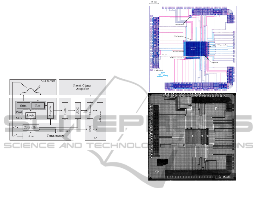
Figure 1: Measurement setup consisting of 5 components.
2.1 CALIBUR
The CALIBUR (see Figure 2) compromises of an
array of 64x64 sensor pixels with a pitch of 12.5 µm
and a sensing electrodes of 4.4 µm x 4.4 µm. These
electrodes are connected directly to the gates of
PMOS measurement transistors, forming the floating
gate. The array of pixels is flanked by 2 digital
decoders, one on the bottom (column decoder) and
one on the left hand side (row decoder). To the right
of the pixel array, amplifier, multiplexer and buffer
circuitry are implemented. The chip has a total size
of 4.8 mm x 4.8 mm, with an active area of 800 µm
x 800 µm. 88 bondpads with integrated electrostatic
discharge protection circuitry surround the perimeter
of the chip. The design, layout and verifying
simulations of all circuits were completed in our
institute using the Cadence IC 5.1.41 software. The
chips were fabricated by ON-SEMI, using the AMIS
0.5 µm 3 metal 2 poly technology. The 3
rd
metal
layer was exclusively used for bondpads and sensing
electrodes in the pixels, while the 1
st
and 2
nd
layers
were used for power, data and control connections.
The size of the pixel elements and their pitch is
chosen to be small enough to have individual
neurons on each one of them. Each pixel consists of
3 transistors; 1 measurement transistor M1 and 2
digital switches M2 and M3 (Figure 3). The gate of
the measurement transistor was connected to the
surface of the chip through vias and metal lines. A
Figure 2: Layout and micrograph of the CALIBUR.
thin-film of a high permittivity material combination
deposited on top of the chip formed the necessary
capacitive coupling between the measurement
transistor and the cells, that would grow on the chip.
In addition to the 64x64 pixel matrix, 2 digital
decoders were integrated on the chip (see Figure 2)
in order to be able to select entire columns (during
read-out) and individual pixels (during stimulation).
Furthermore, the 64 rows of pixels in the matrix
were connected to individual amplifiers to improve
the SNR of the chip. After amplification, the 64 row
signals were put through 8 8x1 multiplexers, which
reduced the number of signals read simultaneously
from 64 to 8. Finally, these 8 signals were sent
through a final stage (output buffer) where the
voltage output of the amplification stage was
converted into a current signal. 8 output pads on the
right hand side of the chip allowed simultaneous
read-out of 8 pixels in the array.
Figure 4 shows the entire signal path following a
single pixel in detail. Each row, as mentioned
before, shares one feedback amplifier. After the 64
signals from the individual rows have been
BIODEVICES 2011 - International Conference on Biomedical Electronics and Devices
416
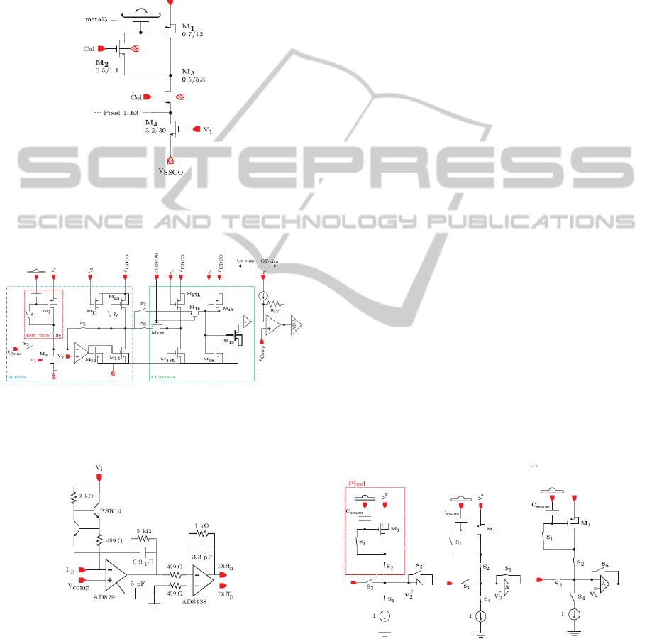
multiplexed down to 8, they are sent through the
output buffer.
The 8 output pads on the chip lead directly to an
additional buffering circuit implemented in the head
stage of the system (Figure 5). The first stage of the
circuitry converts the output current from CALIBUR
into a voltage, while the second stage conditions the
signal for the following step of sampling.
Figure 3: Single pixel in the 64x64 array of CALIBUR.
M4 does not belong to an individual pixel, it is shared by
an entire row of pixels.
Figure 4: Entire signal path of the CALIBUR chip. The 2
operational amplifiers on the right hand side are
implemented off-chip (See Figure 5).
Figure 5: Bufferering and conversion circuitry in the head-
stage.
The pixel circuitry itself can be switched
between 3 different modi during operation:
Calibration, read-out and stimulation (see Figure 6).
Prior to recording of signals, the transistors in the
pixels have to be brought to their optimal points of
operation. This is achieved during the calibration of
the chip. With the switches S1, S2, S4 closed, a
constant current I generated by a single NMOS
transistor is forced through the measurement
transistor M1. Since M1 is in the diode configuration
during the calibration, a charge is accumulated on its
gate, bringing the transistor in the desired operation
point. When the switch S1 is opened, this charge
will have nowhere to flow, thus keeping the
transistor in its preset operation point. In this mode,
with only S2 and S4 closed, the pixel is set in the
record-mode. If there is a change in the electrical
potential on the bottom electrode of the capacitor
formed by the sensing electrode, the thin-film high-k
dielectric deposited on it and the cell cultured on the
chip, this will change the voltage between the gate
and the source of M1, causing its transconductance
to shift. This will change the amount of current
flowing through the pixel. The discrepancy between
the forced current I and the actual current flowing
through the pixel will have to compensated by the
amplifier feedback loop connected to the output of
the pixel. Each row of 64 pixels share one such
amplifier feedback loop. Since both the calibration
and the read-out mode require an entire column to be
selected (and allow only one column to be active at
the same time) by the switch S2, each pixel in the
selected column is directly connected to an
amplifier.
With the switches S1, S2 and S3 closed and S4
opened, the pixel can be operated in the stimulation
mode. In this mode, both the constant current source
and the amplifier feedback loop are disconnected
from the pixel, and the sensing electrode itself
becomes accessible through the port V
stim
. A voltage
applied through V
stim
can be used to stimulate cell
directly on top of the electrodes.
Figure 6: Pixel in calibration mode (A), read-out mode (B)
and stimulation mode (C).
Due to the small area of the sensing electrodes,
the coupling between the cells and the underlying
chip was to be established capacitively. Figure 7
A
B
C
HIGH-DENSITY CMOS ARRAY FOR BI-DIRECTIONAL COUPLING OF ELECTROGENIC CELLS
417

shows a simplified equivalent circuit of the
capacitive coupling and the measurement transistor.
Equation 1 shows, that the capacitive coupling
between the cell and the chip increases with higher
values of C
sense
in a FG-FET configuration. In order
to achieve a high capacitance on an area, that is both
fixed in size and small, the thickness of the dielectric
film deposited on the chip has to be minimized while
its relative permittivity ε
r
needs to be as high as
possible. The results of the electrical characterisation
of this layer are presented in section 4.
Figure 7: Schematic cross-section through a pixel (A) and
simplified equivalent circuit showing the voltage divider
between C
sense
and C
fg
(B).
Equation 1: Coupling of the input voltage to the voltage
across the measurement transistor.
2.2 Head-stage
The head-stage carrying the CALIBUR chip
contains 2 crucial components for the control of all
the digital and analog inputs leading to the chip: The
microcontroller TINY-Tiger 2 (TT2) and the FPGA.
The microcontroller was programmed at the start of
each measurement through a universal serial bus
(USB) interface with parameters the user provided to
the LabView software. All the analog control
voltages shown in the signal path in Figure (V1-4,
Vs) and the VCC’s were given their values by the
TT2. The fast digital signals that controlled the 2
decoders and the multiplexers were set by the
FPGA, which had a step time of 20ns. The
sequencer integrated into the FPGA operated with
40 bit words. 11 bits of these words were used to
implement a repeat routine within the FPGA, which
prolonged to time of the application of a certain
word by the step time multiplied by the value of the
11 bits. This was necessary due to the small physical
memory of the FPGA (2048 x 40 bits) and due to the
fact that each ADC sampling required a trigger sent
by the FPGA. Without the possibility to repeat, it
would be impossible to execute longer
measurements than a few µs.
2.3 ADC
The ADWin-Prolight 2 (Keithley Instruments,
Cleveland, USA) was used as the ADC component
of the measurement setup. 2x14-Bit resolution ADC
modules, each containing 4 separate samplers were
placed into the ADWin, with an on-board memory
of 256 MB per module. The input range was set to ±
3V in order to increase resolution. An external
trigger mechanism was added to the ADC’s in order
to allow the number and timing of the samples to be
determined by the FPGA. The samples were first
saved on the board-memory of the samplers before
being transferred to the user computer for
visualisation and further processing via Ethernet.
3 POST-PROCESSING
Since the operation environment of CALIBUR
demands the chip surface to be in direct contact with
the liquid media the cells are cultivated in, the
passivation of the chip became a very important
issue. Micrographs of the chip after its fabrication
clearly showed cracks in the Si
3
N
4
covering the chip,
which meant, that it would not suffice as a
passivation during cell experiments. Furthermore,
the passivation chosen would also form the coupling
of the sensing electrode with the cells, thus it had to
fulfil the requirement of maximizing the capacitance
formed at the electrode. Equation 1 already shows
that the coupling factor depends on the value of the
sensing capacitance. In order to maximize the
capacitance, while keeping the electrical leakage
through this film as low as possible, several different
methods of deposition and high-k materials were
tested. The deposition method and the material had
to fulfil 5 important specifications:
a) Due to the fact, that the interconnects
were made of aluminium, the temperature
budget for the deposition was limited to
400°C.
b) The deposition method had to be able to
form a uniformly thick film of the
materials deposited on a rough aluminium
electrode surface.
c) The value of the sensing capacitance
should be at least 100 fF.
d) The breakdown voltage should not be less
than 2 V.
A
B
BIODEVICES 2011 - International Conference on Biomedical Electronics and Devices
418

e) The material interfacing the cells must be
bio-compatible
Based on the published data (Schindler et al.,
2007), the deposition method of our choice was the
atomic layer deposition (ALD) due to its excellent
quality of forming very uniform layers on rough
surfaces. ALD is a chemical vapour deposition
(CVD) based method utilizing a self-limiting growth
of the layer being deposited, which allows to grow a
film very slowly (one atomic layer at a time) but
also very uniformly. Figure 8 shows the principle of
deposition with this method: (1) First, gas phased
precursors are brought into the reaction chamber.
During their transport to the substrate surface first
intermediate reactions take place (2-3). The desired
products of these reactions are then adsorbed to the
surface (4) and diffuse to start forming islands which
grow to a closed atomic layer (5-6). Unwanted
product gases are desorbed from the surface (7) and
pumped away (8).
Figure 8: Principle and steps of ALD deposition method.
Obviously, the ALD method was the best
possible choice to fulfil specification b set by the
circumstances. The remaining 4 specifications
depended on the choice of the material or material
combinations deposited with the ALD as well as the
thickness of their film. Several different material
combinations with various thicknesses were
characterised to determine an adequate candidate for
the high permittivity thin film. The characterisation
was done using a 3 electrode potentiostatic system,
with which electrical impedance spectroscopy (EIS)
and cyclovoltammetrical (CV) experiments were
conducted. The system, depicted in Figure 9, was
composed of a measurement cell, which contacted
silicon samples with the high permittivity material
deposited on top of them from the backside, a
potentiostat (PAR 283, Princeton Applied Research),
a Ag/AgCl reference electrode and a Pt counter
electrode. The samples were made of p-Si with very
low resistivity (0,01-0,02 Ωcm) with 100nm of Al
deposited on the front side and 400nm of Al
deposited on the back side. The high permittivity
thin film was deposited on the front side of the 10
mm x 10 mm samples. The measurement cell was
filled with a 100mM NaCl solution to provide
electrical connection between the electrodes inserted
in it.
Figure 9: 3 electrode measurement setup with potentiostat
for CV and EIS experiments.
During EIS experiments, the DC voltage between
the reference electrode and the working electrode,
which was the back contact of the samples in the
measurement cell, was fixed to a constant value,
while an AC pulse of varying frequency was applied
between these electrodes. The current flowing
between the counter electrode and the working
electrode was measured and the complex impedance
of the liquid-oxide interface formed at the surface of
the high permittivity thin film was calculated. The
frequency range of interest was chosen as 100 Hz –
10 kHz.
To find the voltage at which electrical
breakdown of the material occurred and the leakage
current through the film at different DC voltages,
CV experiments were conducted. The reference
electrode kept the electrolyte at a constant potential,
the voltage between the working electrode and the
reference electrode was swept over a given range,
while the current flowing into the working electrode
from the counter electrode was measured. This
current showed the leakage through the high
permittivity film at a given voltage.
4 RESULTS
4.1 High Permittivity Film
To optimize the chips amplification under the given
conditions, we have given great effort to optimize
the high permittivity thin film coating deposited on
the chip. The best results we have achieved so far
were acquired with a triple multilayer deposition of
TiO
2
(TIO) and HfO
2
(HFO). The total thickness of
HIGH-DENSITY CMOS ARRAY FOR BI-DIRECTIONAL COUPLING OF ELECTROGENIC CELLS
419
the triple oxide stack was 126 nm with ( (7 nm HfO
2
+ 35 nm TiO
2
x 3) ). The layers were deposited at a
temperature of 300°C, thus not exceeding the
existing temperature budget of 400°C and hence
fulfilling specification a. The afore mentioned EIS
and CV experiments revealed, that this layer
fulfilled all the other specifications given in the
earlier section as well.
Already published data (Schindler et al., 2007)
shows, that neurons can grow well on HfO
2
. Since
the triple multilayer also has HfO
2
interfacing the
cells, it can be assumed, that specification e will be
met.
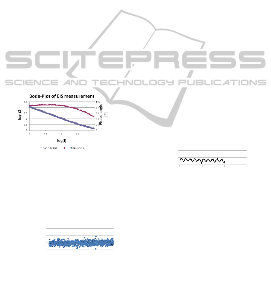
Figure 10 shows the results of the EIS
measurement on a silicon sample deposited with the
triple oxide stack. It was assumed, that the interface
between the oxide and the liquid could be modelled
with a Randles circuit. The capacitance and the film
resistance were calculated by fitting the measured
data to this model. The results show, that the oxide
stack has a compound permittivity of ε
r
= 73, which
leads to a C
sense
= 100.06 fF, which fulfils
specification c.
Figure 10: EIS measurement of the triple multilayer oxide
stack.
Electrical breakdown of the oxide stack was
investigated using the CV method. Figure 11 shows
the electrical leakage through the thin films up to a
voltage of 3 V with 100mV/s, with no electrical
breakdown. This experiment has shown, that the
TIO/HFO triple multilayer also fulfils specification
d.
Figure 11: CV measurement of the triple multilayer oxide
stack.
The results of these experiments have shown,
that the current high permittivity thin film coating of
the CALIBUR fulfils all the requirements necessary
for the chip to function properly.
4.2 Electrical Characterisation
In order to prove the chips and the measurement
systems functionality, the chip, after its
encapsulation was filled with a 100mM NaCl
solution. A Pt wire was inserted into this liquid,
through which electrical pulses could be applied to
the electrodes on the chip. A sine signal with a
frequency of 100 Hz and an amplitude of 4mV was
chosen to record the response of the chip and the
measurement system.
Figure 12 shows the buffered, converted and
sampled output of an electrode on the CALIBUR
(column 31, row 35). Several other electrodes were
also calibrated and used for recording with very
similar results. The converted voltage measures 11
mV in amplitude with a frequency of 100 Hz. The
output current leaving the CALIBUR was calculated
as 348 µA, which is close to the simulated value of
320 µA. The input sine signal was assumed to be an
offset-free AC signal, which is hard to achieve
during the experiment because of the existence of
DC potentials on the electrodes due to the double
layer forming at the liquid-oxide interface. This may
have lead to the discrepancy between the simulated
value of the output current and the measurements.
Figure 12. Buffered, converted and sampled response of
the CALIBUR and the measurement system to a 100 Hz, 4
mV amplitude sine wave.
5 CONCLUSIONS
In this work we presented a CMOS chip with a
64x64 array of electrodes at a pitch of 12.5 µm and a
size of 4.4 µm x 4.4 µm. Digital circuitry allowing
the exact addressing of entire columns for recording
and calibration, as well as individual pixels for
stimulation were integrated on the chip.
Furthermore, a feedback amplifier circuitry was
implemented on the chip to enhance the measured
signals. A post-processing step to deposit a thin film
‐5,00E‐09
0,00E+00
5,00E‐09
1,00E‐08
0123
Current[A]
Voltage[V]
0,00
0,10
0,20
0,70 0,75 0,80 0,85
Voltage[V]
Time[s]
BIODEVICES 2011 - International Conference on Biomedical Electronics and Devices
420

high-permittivity material on the chip is also
explained and the best results of this endeavour are
shown.
The measurement system to operate the chip was
also explained in detail.
The functionality of the chip was proven
electrically. Biological experiments will follow
shortly to verify its capability to measure from
cardiomyocyte cultures grown in vitro.
REFERENCES
Thomas, C., Springer, P., Loeb, G., Okun, L., 1972, A
miniature microelectrode array to monitor the
bioelectric activity of cultured cells, Exp. Cell Res.,
74, pp. 61-66
Pine, J., 1980, Recording action-potentials from cultured
neurons with extra-cellular micro- circuit electrodes,
Journal of Neurosience Methods, 2, pp. 19-31
Gross, G., Williams A., 1982, Recording of spontaneous
activity with photoetched microelectrode surfaces
from mouse spinal neurons in culture, Journal of
Neuroscience Methods, vol. 5, pp. 13-22
Heer, F., Hafizovic, S., Franks, W., Blau, A., Ziegler C.,
Hierlemann A., 2006, IEEE Journal of Solid-State
Circuit, 41, 1620
Heer, F., Franks, W., Blau, A., Taschini S., Ziegler C.,
Hierlemann, A., Baltes H., 2004, Biosensors and
Bioelectronics, 20, 358
Eversmann, B., Jenkner, M., Hofmann, F., Paulus, C.,
Brederlow, R., Holzapfl, B., Fromherz, P., Merz, M.,
Brenner, M., Schreiter, M., Gabl, R., Plehnert, K.,
Steinhauser, M., Eckstein, G., Schmitt-Landsiedel, D.,
Thewes, R., 2003, IEEE Journal of Solid-State
Circuit, 38, 2306
Hofmann, F., Eversmann, B., Jenkner, M., Frey, A., Merz,
M., Birkenmaier, T., Fromherz, P., Schreiter, M.,
Gabl, R., Plehnert, K., Steinhauser, M., Eckstein, G.,
Thewes, R., 2003, ESSDERC 2003, Proc. 33rd
European Solid- State Device Research Conference,
167
Meyburg, S., Stockmann, R., Moers, J., Offenhaeusser, A.,
Ingebrandt, S., 2007, Sensors Actuators B
Meyburg, S., Goryll, M., Moers, J., Ingebrandt, S.,
Böcker-Meffert, S., Lüth, H., Offenhaeusser, A., 2006,
Biosensors and Bioelectronics, 21, 1037
Meyburg, S., Wrobel, G., Stockmann, R., Moers, J.,
Ingebrandt, S., Offenhaeusser, A., 2006, Applied
Physics Letters, 89, 013901
Imfeld, K., Neukom, S., Maccione, A., Bornat, Y.,
Martinoia, S., Farine, P-A., Koudelka-Hep, M.,
Berdondini, L., 2008, IEEE Transactions on
Biomedical Engineering, 55, 2064
Schindler, M., Kim, S.K., Hwang, C.S., Schindler, C.,
Offenhaeusser, A., Ingebrandt, S., 2007, Rapid
Research Letters, phys. stat. sol. 2, No. 1, 4-6, DOI
10.1002/pssr.200701242
HIGH-DENSITY CMOS ARRAY FOR BI-DIRECTIONAL COUPLING OF ELECTROGENIC CELLS
421
