
BIOINSPIRED SENSORY INTEGRATION FOR
ENVIRONMENT-PERCEPTION EMBEDDED SYSTEMS
Jordi Madrenas, Daniel Fernández, Jordi Cosp, J. Manuel Moreno
Luis Martínez-Alvarado and Giovanny Sánchez
Electronic Engineering Department, Universitat Politècnica de Catalunya, C4 Building
Jordi Girona 1-3, 08034 Barcelona, Catalunya, Spain
Keywords: Bioinspired Systems, MEMS, MEMSoC, Integrated Systems, Sensors, Environment Perception.
Abstract: In this work, the architecture of a system intended for bioinspired environment perception is described.
Considering the technology trends and applications requirements, the properties of such a system are
discussed. The system consists of four main blocks: a) A set of different integrated microsensors and
microactuators with the associated signal conditioning circuits; b) A data encoding block that in its simplest
form performs spike encoding of information; c) a bioinspired digital processing block that efficiently
emulates a spiking neuron network; d) a monitoring and self-adaptation block that provides feedback to the
sensors and actuators. In its final implementation, the full system would eventually be almost fully
integrated in a CMOS integrated circuit.
1 INTRODUCTION
In the latest decades, impressive advances in
Information and Communication Technologies
(ICTs) have led computing and network
collaboration to unsuspected limits.
The combination of continued progress in
microelectronics, , Micro-Electro-Mechanical sensor
and actuator Systems (MEMS), wireless
communications, signal processing, power
management and software engineering enables the
development of small-size yet complex autonomous
systems working in distributed computing networks
capable of interpreting physical environment and to
interact with it.
As existing state-of-the-art CMOS technology
generations improve, still more computing capacity
will be available. Moreover, emerging new
nanotechnologies promise in an uncertain future a
computing capability that would by far exceed the
currently available performance. Let us review some
key aspects related with computing approach and
interaction with the environment.
1.1 Ubiquitous Computing
The ambitious goal of achieving a ubiquitous
computing network (pervasive network computing)
is the common denominator of many recent and
current research efforts.
When the emphasis is on miniaturization,
systems including sensing capability, processing,
self-powered and communication skills are called
smart dust
(Warneke, B. et al., 2001), smart nodes or
Wireless Sensor Networks (WSN) (Akyildiz I. F. et
al., 2002) as Spec devices (Hill, J. et al., 2000), CCR
(Hollar S. E. A., 1996), MoteTrack (Lorincz K. and
Welsh M., 2006) and Intel Mote (Nachman, L. et al.,
2005) among others (Wong, A. C. W. et al., 2008),
(Takeuchi, T. et al., 2009), that allow to build
distributed wireless sensor networks.
As a result of all the developed research activity,
nowadays, several powerful wireless sensor nodes
are commercially available.
1.2 Microsensors and Microactuators
Micro-Electro-Mechanical Systems (MEMS, or
NEMS if their size reduces to the nanoscale) can be
defined as integrated devices that combine electrical,
mechanical and optical components (Senturia S. D.,
2001; Gad-el-Hak M., 2001). Their size ranges from
microns to millimeters and they are manufactured
using processes similar to integrated circuits, but in
general not compatible, that allow to selectively
remove parts of the silicon wafer or add new
260
Madrenas J., Fernández D., Cosp J., Moreno J., Martínez-Alvarado L. and Sánchez G..
BIOINSPIRED SENSORY INTEGRATION FOR ENVIRONMENT PERCEPTION EMBEDDED SYSTEMS.
DOI: 10.5220/0003190202600267
In Proceedings of the International Conference on Biomedical Electronics and Devices (BIODEVICES-2011), pages 260-267
ISBN: 978-989-8425-37-9
Copyright
c
2011 SCITEPRESS (Science and Technology Publications, Lda.)

structural layers. MEMS can act as sensors or
actuators, either individually or in arrays, to produce
effects on a larger scale.
Currently, there is a large number of different
MEMS. Non-comprehensive examples are pressure
and displacement sensors, accelerometers,
gyroscopes, cantilevers, precision instruments,
manipulators, micro-relays, micromirrors, thermal,
chemical, micro-fluidics, etc. Each MEMS device
requires its own electronic circuitry, based on
characteristic frequency, load, voltage and current
levels, noise, etc. For instance, for a capacitive
accelerometer the resonance frequency ranges in the
order of tens of kHz, bandwidth of several kHz,
under a 6 V supply. For an angular quartz sensor, the
vibration is of some kHz and bandwidth over 50 Hz,
with voltage over 5 V. Other kinds of MEMS
require much higher frequency, such as those
operating in RF. In electrostatic actuators, voltage
requirements may be tens of volts or more.
Therefore, treatment should be completely different
for each particular case.
Besides the previous consideration, MEMS
sensors and actuators characteristics variation with
aging, temperature, humidity or other physical
phenomena, as well as reliability, raise the need for a
self-adaptive conditioning systems.
Therefore, MEMS/NEMS already offer and
promise more interaction with the environment at
micro/nano scale. Thus, embedded in computing
nodes, reduced-size and low-power systems able to
interact with the environment become feasible.
MEMS technologies are not CMOS compatible
in general, so further integration is limited from this
point of view. Several research efforts in developing
compatible CMOS MEMS have been done in the
latest years, as it will be discussed (Baltes H. et al.,
2002; Brand O. et al., 2005).
1.3 Self-adaptation and Bioinspiration
Despite technology already offers powerful
computing and sensing devices, artificial algorithms
still are limited in the extent of environment
interaction capabilities, compared with even the
simpler existing living beings.
The inspiration more directly related to
environment perception is the autonomous function
of the human central nervous system. The human
autonomous control employs motor neurons to send
indirect messages to organs at a subconscious level.
These messages regulate unconscious processes and
variables such as temperature, breath, heartbeat or
digestion, among many others. The parallel for
artificial systems is a network of processors which
performs the necessary operations at the right time
without the need of dedicated attention, in the so-
called autonomic computing paradigm (Kephart, J.
O.; Chess, D. M., 2003).
Such computing paradigm changes from the
conventional processing power to another one driven
by data. Besides the traditional centralized storage,
access to data from multiple distributed sources
enable users to access to information when and
where needed. The main objectives of these
distributed and autonomous architectures are often
referred to as self-* properties. Systems able to self-
manage should be self-configuring, self-healing,
self-optimizing, and self-protecting and exhibit self-
awareness, self-situation, self-monitoring, and self-
adjustment (Dobson, S. et al., 2010). Thus, the
information they can provide from the physical
environment they are immersed is essential for those
systems.
In addition to the autonomic computation
proposal, there are many other similar approaches,
for example Organic Computing (Gudemann, M. et
al. 2008) Systemic Computation (Bentley, P. J.,
2007) and Æther (Soto, V. J. et al., 2009).
Due to the power and interconnect limitations,
increased processor performance is nowadays
coming more from the increasing computing
parallelism rather than from clock frequency
improvements. The nanometer-size cutting-edge
VLSI devices suffer from great variability and non-
ideal effects. Further, with reduced dimensions,
cosmic radiation-produced soft errors start to appear
also at ground level. For these reasons, very serious
reliability issues arise and a holistic strategy for fault
tolerance and self-repair is required.
Because of their nature, bio-inspired neural
networks promise feasible solutions: they are
constructed with slow and unreliable elements, they
are tolerant to manufacturing defects and to noisy
environments, they are robust in the presence of
hardware failures, they are not programmed but they
adapt and self-organize, and they interact with the
real world.
Based on studies of the human cortex the fields
of computer science and cognitive neuroscience
have been combined from a top-down approach
(Hawkins J. and Blakeslee S., 2004). It is
conjectured that the resolution of complex
perception problems is done by means of few layers
of neurons, evenly distributed and massively parallel
working further massively interconnected with direct
and feedback flows of information. The ability to
predict is what sets the human intelligence and it is
BIOINSPIRED SENSORY INTEGRATION FOR ENVIRONMENT-PERCEPTION EMBEDDED SYSTEMS
261

based on recording pattern sequences, in self-
associative recovery, to capture invariant
representations in the organizational hierarchy (but
uniform) of cognitive tasks and decision taken with
Bayesian criteria.
1.4 Bioinspired Devices
In the context of sensor nodes and bio-inspired
computing, in the Perplexus project (Upegui A. et
al., 2007) the ubidule was defined as a UBIquitous
computing moDULE with high computing power
(sequential control processor combined with
powerful programmable logic) and networked
external communication, wired or wireless, with a
large number of peers. The difference with other
proposed sensor nodes is that the ubidules include
bioinspired mechanisms. Among several modes of
operation, the ubidule can emulate massively-
parallel bioinspired spiking neural networks
(Madrenas J., Moreno J. M., 2009).
In its current implementation, the ubidule is a
purely digital processing device and it can use only a
very limited number of standard sensors with high
consumption and low bandwidth, sufficient for
demonstration but not for advanced applications.
Thus, it would require a parallel acquisition system
which allows the massive use of sensors and
actuators, as well as encoding information in pre-
processed data streams treatable by ubidules.
In this paper, the NESSIE (Neural and Self-
adaptive Sensory Integration for Environment
Perception Embedded Systems) architecture is
introduced. NESSIE systems enhance the ubidule
functionality by providing integrated microsensors
and actuators as well as a mixed-signal information
pre-processing and self-adaptation, thus enabling
simple environment interaction in the initial
versions, and allowing scaling to complex
applications.
In Section 2, the NESSIE architecture is
proposed. In the following sections, the different
parts are introduced: the proposed integrated
microsensors and actuators and their conditioning
circuits (Section 3), the data encoding block (Section
4), the boinspired digital processing block (Section
5) and the monitoring and self-adaptation blocks
(Section 6). In Section 7, a possible application is
pointed out. Finally, in Section 8, conclusion and
future work are detailed.
2 THE NESSIE ARCHITECTURE
As discussed in the introduction, an artificial system
able to exhibit some extent of environment
perception and interaction should endow sensory
elements and some kind of bioinspired or biological-
like information processing. Furthermore, given the
complexity of biological systems, that provide an
extraordinary degree of redundancy and parallelism,
one of the main efforts in developing such artificial
systems should consider integration as a
fundamental issue. In the direction of the ultimate
objective of biological system emulation, this work
proposes one step of microsensors and actuators
integration in the CMOS technology, as well as the
full system architecture that embeds bioinspired
information processing. The extrapolation of this
work to future more advanced technologies would
allow the development of low-power, reduced-size
environment perception devices.
In Fig. 1, the block diagram of the NESSIE
environment perception embedded system is shown.
CONDITIO-
NING
CONDITIO-
NING
CONDITIO-
NING
MONITOR
EXTERNAL
SENSORS
CONDITIO-
NING
PREPRO-
CESSING:
DATA
ENCODING
UBIDULE
BIOINSPIRED
DIGITAL
PROCESSING
INT EGRATED
SENSORS
(& ACTUATORS)
SELF-ADAPTATION
AER
BUS
EXTERNAL
COMMUNICATION
Figure 1: The NESSIE architecture.
It consists of the following elements:
A set of different integrated sensors that could
be either individual or arrays of them. External
sensors could be provided as well when
integration is not possible. Specific for each
class of sensor, signal conditioning associated
circuits provide the transduced information in
proper electric form.
Data encoding block. It is a preprocessing
analog block that in its simplest form performs
spike encoding of information; however, it can
be extended to also perform data
compression/fusion.
Bioinspired digital processing block.
Monitoring and self-adaptation blocks.
BIODEVICES 2011 - International Conference on Biomedical Electronics and Devices
262

Whereas the ultimate goal is to integrate the
whole NESSIE system in a single chip, in the
present proof-of-concept, the analog blocks are
integrated in different chips from the ubidule, which
is purely digital. Furthermore, the present
implementation of the ubidule mainly consists of a
bioinspired chip and a separate microcontroller.
3 CMOS INTEGRATED
SENSORS AND ACTUATORS
Nanometer-size CMOS technology currently allows
to integrate very complex SoCs (System-on-Chip) in
a single silicon die. Integrating microsensors or
microactuators, however, is a much more
challenging task, because of manufacturing process
compatibility.
3.1 Transducers
A number of different CMOS-compatible sensors
can be currently integrated in a CMOS-technology
silicon die. Some of them are:
Optical integrated photodetectors. Based on the
photodiode, the CMOS photodetectors are a
mature technology that allow for the
implementation of linear- and 2D-array
cameras in CMOS substrate. Furthermore,
many conditioning circuits have been proposed
that allow a logarithmic response of the sensor
in order to accommodate the large dynamic
range of visible light.
Temperature sensors. By means of parasitic
bipolar transistors, high performance
temperature sensors can be implemented in
CMOS (Matranga G. et al., 2002; Udrea, F. et
al., 2008). Also, temperature sensors based
exclusively on MOS transistors have been
reported (Prakash S. B et al., 2006; Ren Y. et
al., 2009).
Magnetic sensors. CMOS compatible based on
the Hall effect and integrated magnetic
concentrators, e.g. (Randjelovic, Z. B. et al.,
2002).
Pressure sensors. These devices are
implemented by means of standard CMOS
silicon die micromachined after the CMOS
processing (Zhou M. X. et al., 2004).
Electrostatic capacitive sensors and actuators.
Several experiments have been done to obtain
CMOS-compatible electrostatic actuators. In
particular, we have designed a number of
structures in standard 0.35 micron CMOS
technologies. Using the metal layers to build
electrostatic actuators and the inter-metal
silicon dioxide as sacrificial layers, membranes
and cantilevers were designed. After this, the
sacrificial material is selectively removed
through windows opened on the passivation
layer mask of the same manufacturing process
by means of a wet or gas etchant (Fernández D.
et al., 2010).
In Fig. 2, an interferometer image of a
membrane obtained with the indicated release
process is shown.
In the present work, focus has been directed to
photodetectors, temperature sensors and electrostatic
MEMS.
Figure 2: Standard-CMOS electrostatic membrane MEMS.
3.2 Signal Conditioning Circuits
As it is well-known, the signal conditioning circuits
are very transducer-dependent. The sensed physical
variable is transduced either to current, charge or
voltage form and information is carried in the
magnitude value or some signal property, as for
instance frequency.
For the case of optical photodetectors, in order to
provide broad dynamic range, logarithmic-response
circuits are mostly used, this requires specific
circuits developed for this purpose (Delbruck T.,
2004; Guo J., Sonkusale, S., 2009; Wang C., 2010).
Concerning electrostatic MEMS sensors for
accelerometers, a capacitive Wheatstone bridge
output signal can be amplified by means of
continuous-time voltage and classic instrumentation
amplifier-based circuits, optimized by means of
synchronous modulation (Lemkin, M., 1999) or
switched-capacitor offset compensation (Wu J.,
2004). Alternatively, the transducer information can
be directly encoded in frequency by means of
relaxation oscillators and a high-precision digital
frequency demodulator based on counters (Michalik
P. et al., 2010).
Similarly, temperature sensor conditioning can
be done by means of a fully-analog or some mixed-
BIOINSPIRED SENSORY INTEGRATION FOR ENVIRONMENT-PERCEPTION EMBEDDED SYSTEMS
263

signal (or mostly-digital) approach
(Park S, 2009;
Woo K, 2009).
Taking into account the steady CMOS down-
scaling it seems that mixed-signal circuits operating
mostly as digital devices (switches) are more likely
to adapt to the limited characteristics of nanoscale
transistors.
4 DATA ENCODING BLOCK
As from the sensors output signals the physical
value is represented by means of a voltage or
current, this block performs a translation into a form
that is feasible to apply as input to a spiking neural
network. The most straightforward is to encode
information in the frequency domain and from there
to a spiking stream, although this is not the only
possibility.
For instance, a low-power spike event
coding/decoding scheme for transmission of analog
signals that uses a reduced number of transitions in
signals with low high-frequency components has
been proposed (Gouveia, L. C. et al., 2009) and
could be applied as a more sophisticated encoding
strategy.
Spikes are then transmitted to the bioinspired
digital processing block by means of synchronous
address-event representation (AER) (Sivilotti M.,
1991), (Moreno, J. M. et al., 2009). In this protocol,
each spike is encoded indicating a sensor label
(address) that uniquely identifies its origin and
permits routing it to the destination neuron input
synapse, using the same physical communication
bus for all inputs. Thus, all the spikes from the
different sensors are transmitted through the same
AER bus and they are connected to the spiking
neural network inputs by means of a packet-
switching scheme.
5 BOINSPIRED DIGITAL
PROCESSING BLOCK
As indicated in the Introduction and shown in Fig. 1,
the NESSIE architecture includes bioinspired
processing based on spiking neural networtks
(SNN). The basic element is the so-called ubidule,
that embeds a microcontroller (sequential control
processor), an application-specific integrated circuit
called ubichip (that can be either an FPGA or a
custom chip) that accelerates the emulation of SNNs
and external wired or wireless communication
channels to be able to interact with other ubidules.
In Fig. 3, the multiprocessor ubichip architecture
is shown. The ubchip architecture combines
parallelism and time multiplexing in a balanced
form:
Neuron input synapses are time-multiplexed
and executed by the same physical processing
element (PE).
Neurons are parallel-emulated, each one by the
same PE that previously executed the algorithm
corresponding to its input synapses.
All PEs (processing Elements) operate
synchronously in a SIMD (Single-Instruction
Multiple-Data) scheme. The PE consists of a
simple 16-bit ALU and two 8-register banks.
The ubichip contains a 10×10 PE-array, a
sequencer, an AER bus controller, a
configuration unit to program the device and an
interface to the microprocessor. External RAM
and a Content-Addressable Memory (CAM) are
also required.
The sequencer block fetches instructions from
the external SRAM memory and broadcasts
them to the PE array. The SRAM is also used to
store the SNN parameters, both neurons and
synapses.
The spiking neuron model assumes a pulsed
binary output, with long steady times and short
pulses. These output spikes are time-
multiplexed and broadcasted to all neurons by
means of a global AER bus. As indicated
before, the same AER bus is used as input for
the incoming spikes generated by the sensory
encoding.
The CAM (Content-Addressable Memory)
decodes the spike address and generates an
input spike to the neuron synapses being
connected to that output spike.
Ubichip
Configura-
tion unit
Sequencer
SRAM
512x32
CAM
µP interface
AER bus
to other Ubichips
CAM/AER
controller
to other Ubichips
PE
PE
PE
PE
PE
PE
PE
PE PE
Figure 3: Multiprocessor ubichip architecture.
The digital processing block is thus able to
perform bioinspired processing of the sensor
BIODEVICES 2011 - International Conference on Biomedical Electronics and Devices
264
information. Learning from the inputs is done by
means of the previous experience, by self-adaptation
of synapses. The platform is flexible enough to
support multi-model implementation of SNNs
(Hauptvogel M. et al., 2009).
Figure 4: Example of emulated membrane potential over
time of six neurons in a 6x6 neuron array.
In its current proof-of-concept implementation, a
6x6-PE array, each one emulating a neuron, has
been mapped on a Xilinx Spartan xc3s5000 FPGA.
Once programmed, the FPGA configuration is
locally controlled by means of an Xscale PXA270
processor operating under Linux. An Ethernet
connection allows sending commands from a
terminal (Upegui A. et al., 2007).
Two different bioinspired spiking neural models
(Iglesias J. et al. 2005, Izhikevich E. M., 2006) have
been encoded in the multiprocessor using specific
software development tools (Hauptvogel M. et al.,
2009). The system programmability allows the
implementation and parallel emulation of virtually
any spiking neuron model.
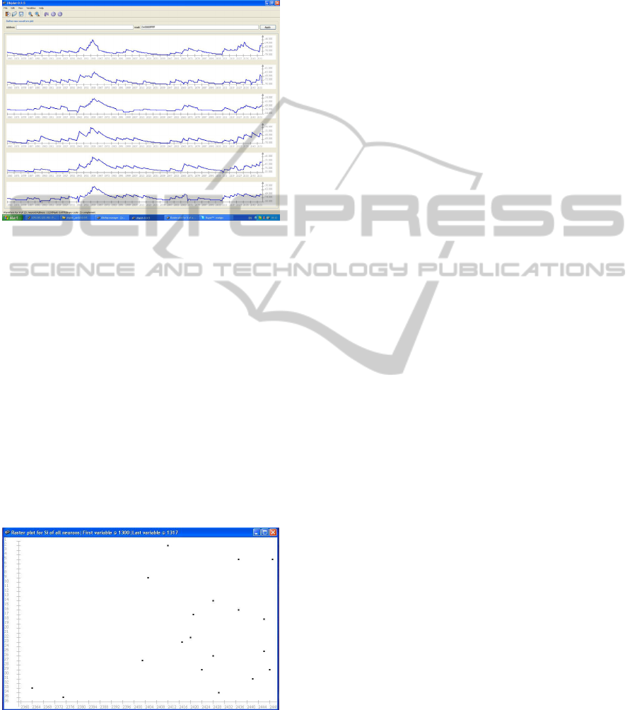
Figure 5: Example of emulated spike raster plot over time
in a 6x6 neuron array.
As an example, figures 4 and 5 display,
respectively, the membrane potential and spike
raster plot snapshots of the 6x6 spiking neural
network emulation of one of the Iglesias model.
6 MONITORING
AND SELF-ADAPTATION
BLOCKS
The monitor is in charge of analyzing the signal
acquisition process. As a function of the outputs and
also from the bioinspired digital processing block
outputs, it can decide modifying the sensor
distribution. For instance, activate/deactivate some
of them, increasing the number or their sensitivity.
The self-adaptation block regulates the sensors
signal conditioning blocks as a function of the signal
output and the monitor commands.
7 CONCLUSIONS
AND FUTURE WORK
Present and coming micro- and nano-technologies
challenges started conditioning the way data
processing and environment interaction are
performed for building intelligent systems. Together
with the increasing difficulty of implementing fully-
deterministic systems in terms of reliability and
operation and power and size constraints,
conventional artificial systems show limited
capability to perform environment perception tasks,
at least compared with biological beings.
Taking into account these constraints, the
proposed approach combines integration of
electronic computing devices, sensors and actuators
together with mostly-digital signal conditioning and
bioinspired computation.
The mostly-digital (or mixed-signal) approach
may be at the cost of individual sensor performance,
but, consistently with bioinspiration and technology
integration, the use of parallelism may compensate
in this tradeoff.
The NESSIE architecture targets to this
paradigm. It has been introduced as a proposal of
new generation of artificial bioinspired systems,
with capability of environment perception and
interaction.
The main features of the NESSIE architecture
are:
CMOS integration of sensors and electronics,
which allow reduced system size and low
power consumption.
BIOINSPIRED SENSORY INTEGRATION FOR ENVIRONMENT-PERCEPTION EMBEDDED SYSTEMS
265

Encoding all sensor outputs in a common
spiking form.
Bioinspired digital processing using SNN
algorithms which supports learning from the
sensors past experience.
Sensor adaptation to compensate for variations
and aging.
As an application example of the NESSIE
architecture, a system that contains the following
elements is under development:
A linear array of 10 photodetectors with
logarithmic detection circuit.
A temperature sensor with voltage output.
An accelerometer with frequency output.
Conditioning circuits with spike stream for all
the sensors.
Asynchronous-to-synchronous AER bus
adaptation.
A ubidule element.
System monitor and self-tuning circuit for
linear photodetector array mismatch and sensor
aging compensation.
When available, the complete system will be
ready to be used in robotic applications. In this case,
the robots can learn from incoming previous
conditions, such as the correlation between the
vibration and light conditions.
In next NESSIE system implementations,
microactuators can be used for a full environment
interaction, leading ultimately to MEMSoC (Micro
Electro Mechanical System on Chip) devices.
ACKNOWLEDGEMENTS
This work has been partially funded by the Spanish
Ministry of Science and Innovation project
TEC2008-06028/TEC. Luis Martinez-Alvarado and
Giovanny Sánchez hold research fellowships
supported by the Catalan Department of Innovation,
Universities and Companies, and the European
Social Fund (ESF).
REFERENCES
Akyildiz I. F. et al., 2002, Wireless sensor networks: a
survey, Computer Networks, Vol. 38, Issue 4, 15
March 2002, pp. 393-422.
Baltes H. et al., 2002. CMOS MEMS-present and future.
Micro Electro Mechanical Systems, 2002. The
Fifteenth IEEE International Conference on. IEEE;
2002:459–466.
Brand O. and Fedder G. K. eds CMOS-MEMS, Advanced
Micro & Nanosystems (Vol. 2). Weinheim: Wiley-
VCH; 2005:596.
Bentley, P. J. 2007. Systemic computation: A model of
interacting systems with natural characteristics. Int. J.
Parallel Emerg. Distrib. Syst. 22, 2 (Mar. 2007), 103-
121.
Delbruck T., Oberhoff D. Self-biasing low power adaptive
photoreceptor. 2004 IEEE International Symposium
on Circuits and Systems. 2004:IV-844-7.
Dobson, S. et al., 2010. Fulfilling the Vision of Autonomic
Computing. Computer, vol.43, no.1, pp.35-41, Jan.
2010.
Fernández D. et al., 2010. Experiments on the Release of
CMOS-Micromachined Metal Layers. Journal of
Sensors, vol. 2010, Article ID 937301, 7 pages, 2010.
Gad-el-Hak M., 2001. The MEMS Handbook, (Editor)
CRC; 1st edition, September 27, 2001.
Gouveia, L. C. et al., 2009. A CMOS implementation of a
spike event coding scheme for analog arrays. Circuits
and Systems, 2009. ISCAS 2009. IEEE International
Symposium on, pp.149-152, 24-27 May 2009.
Gudemann, M. et al. 2008. A Specification and
Construction Paradigm for Organic Computing
Systems. Self-Adaptive and Self-Organizing Systems,
2008. SASO '08. Second IEEE International
Conference on, pp.233-242, 20-24 Oct. 2008.
Guo J., Sonkusale, S., 2009. A High Dynamic Range
CMOS Image Sensor for Scientific Imaging
Applications. Sensors Journal, IEEE. Vol. 9, Iss. 10,
2009, pp. 1209 – 1218.
Hauptvogel M. et al., 2009. SpiNDeK: An Integrated
Design Tool for the Multiprocessor Emulation of
Complex Bioinspired Spiking Neural Networks. IEEE
Congress on Evolutionary Computation (CEC 2009).
18-21 May, 2009, pp.142-149.
Hawkins J., Blakeslee S., 2004. On intelligence. Times
books, Henry Holt and Company, 2004.
Hill, J. et al., 2000. System architecture directions for
networked sensors. SIGPLAN Not. 35, 11 (Nov.
2000), pp. 93-104.
Hollar S. E. A., 1996. COTS Dust, B.S. Mass.Inst. of
Tech., http://siliconrobot.com/publications/cotsdust.
pdf.
Iglesias J. et al. 2005. Dynamics of pruning in simulated
large-scale spiking neural networks, Biosystems,
Volume 79, Issues 1-3, Pages 11-20.
Izhikevich E. M., 2006. Polychronization: Computation
with Spikes. Neural Computation, Vol. 18, No. 2. (1
February 2006), pp. 245-282.
Kephart, J. O.; Chess, D. M., 2003. The vision of
autonomic computing. Computer, vol.36, no.1, pp. 41-
50, Jan 2003.
Lemkin M, Boser B. E. A three-axis micromachined
accelerometer with a CMOS position-sense interface
and digital offset-trim electronics. IEEE Journal of
Solid-State Circuits. 1999;34(4):456-468.
Lorincz K. and Welsh M., 2006. MoteTrack: A Robust,
Decentralized Approach to RF-Based Location
Tracking, Personal and Ubiquitous Computing,
BIODEVICES 2011 - International Conference on Biomedical Electronics and Devices
266

Special Issue on Location and Context-Awareness,
Springer-Verlag, October 2006.
Madrenas J., Moreno J. M., 2009. Strategies in SIMD
Computing for Complex Neural Bioinspired
Applications. NASA/ESA Conference on Adaptive
Hardware and Systems, AHS, pp. 376-381, 2009.
Matranga G, et al., 2002. CMOS temperature sensor. US
Patent 6, 489, 831. 2002.
Michalik P, et al., 2010. Technology-portable mixed-
signal sensing architecture for CMOS-integrated z-
axis surface-micromachined accelerometers. Mixed
Design of Integrated Circuits and Systems (MIXDES),
2010 Proceedings of the 17th International
Conference. 2010:431-435.
Moreno J. M. et al., 2009. Synchronous Digital
Implementation of the AER Communication Scheme
for Emulating Large-Scale Spiking Neural Networks
Models. Adaptive Hardware and Systems, 2009.
NASA/ESA Conference on, pp.189-196, July 29 2009-
Aug. 1 2009.
Nachman, L. et al., 2005. The Intel® mote platform: a
Bluetooth-based sensor network for industrial
monitoring. Information Processing in Sensor
Networks, 2005. IPSN 2005. Fourth International
Symposium on, vol., no., pp. 437- 442, 15 April 2005.
Park S, Min C, Cho S, 2009. A 95nW ring oscillator-based
temperature sensor for RFID tags in 0.13µm CMOS.
Circuits and Systems, 2009. ISCAS. 2009.
Prakash S. B., Cohen M. H., Abshire P. A. Detection of
on-chip temperature gradient using a 1.5V low power
CMOS temperature sensor. 2006 IEEE International
Symposium on Circuits and Systems. 2006:1171-1174.
Randjelovic, Z. B. et al., 2002. Highly sensitive Hall
magnetic sensor microsystem in CMOS technology.
Solid-State Circuits, IEEE Journal of, vol.37, no.2,
pp.151-159, Feb 2002.
Ren Y, Wang C, Hong H., 2009. An All CMOS
temperature sensor for thermal monitoring of VLSI
circuits. ICTD 2009. IEEE Circuits. 2009.
Senturia S. D., 2001, Microsystem Design, Kluwer
Academic Publishers; Jan. 2001.
Sivilotti M., 1991. Wiring Considerations in Analog VLSI
Systems With Applications to Field Programmable
Networks, Ph.D. dissertation, California Institute of
Technology, Pasadena, 1991.
Soto, V. J.; et al., 2009. Implementation of a Dynamic
Fault-Tolerance Scaling Technique on a Self-Adaptive
Hardware Architecture, Reconfigurable Computing
and FPGAs, 2009. ReConFig '09. International
Conference on, pp.445-450, 9-11 Dec. 2009.
Takeuchi, T. et al., 2009. A single-chip sensor node LSI
with synchronous MAC protocol and divided data-
buffer SRAM. International SoC Design Conference
(ISOCC), pp.202-207, 22-24 Nov. 2009.
Udrea, F. et al., 2008. CMOS temperature sensors -
concepts, state-of-the-art and prospects.
Semiconductor Conference, 2008. CAS 2008.
International , vol.1,, pp.31-40, 13-15 Oct. 2008.
Upegui A. et al., 2007. The Perplexus bio-inspired
reconfigurable circuit. Second NASA/ESA Conference
on Adaptive Hardware and Systems (AHS 2007), pp.
600-605, IEEE 2007.
Wang C., 2010. Wide-Dynamic-Range and High-
Sensitivity Current-to-Voltage Converters. Circuits,
Systems and Signal Processing. 2010; 29(6):1223-
1236.
Warneke, B. et al., 2001. Smart Dust: communicating with
a cubic-millimeter computer, Computer, vol.34, no.1,
pp.44-51, Jan 2001.
Wong, A. C. W. et al., 2008, A 1 V Wireless Transceiver
for an Ultra-Low-Power SoC for Biotelemetry
Applications. Solid-State Circuits, IEEE Journal of,
vol.43, no.7, pp.1511-1521, July 2008.
Woo K, Meninger S, Xanthopoulos T, E. Dual-DLL-based
CMOS all-digital temperature sensor for
microprocessor thermal monitoring. Solid-State
Circuits, ISSCC, Vol 40; 2009:68-70
Wu J, Fedder G, Carley L. A low-noise low-offset
capacitive sensing amplifier for a 50-μg/√ Hz
m
onolithic CMOS MEMS accelerometer. Solid-State
Circuits, IEEE. 2004; 39 (5):722-730.
Zhou M.X. et al., 2004. A fully CMOS compatible
integrated absolute pressure sensor. Solid-State and
Integrated Circuits Technology, 2004. Proceedings.
7th International Conference on, vol.3, pp. 1816-
1819, 18-21 Oct. 2004.
BIOINSPIRED SENSORY INTEGRATION FOR ENVIRONMENT-PERCEPTION EMBEDDED SYSTEMS
267
