
FREQUENCY CHARACTERIZATION OF A MAGNETICALLY
ACTUATED MEMS RESONANT BIOSENSOR
V. Russino, F. Pieri
Dipartimento di Ingegneria dell’Informazione, Universit
`
a di Pisa, Via G. Caruso 16, 56122 Pisa, Italy
D. Paci
STMicroelectronics, Via Tolomeo 1, 20010 Cornaredo, Italy
Keywords:
Biosensors, Resonant sensors, Microbalances, MEMS.
Abstract:
In this work, the mass response of a resonant, CMOS (Complementary MOS) compatible MEMS sensor,
oriented at the detection of diagnostic markers, is presented. The sensor is fabricated with a MEMS (Micro-
electro-mechanical System) post-processing method on a standard, CMOS-based VLSI technology, retaining
maximum compatibility with the CMOS process flow. The mechanical resonator is based on inductive actu-
ation and detection, and the sensing is based on the microbalance principle. A protocol for covalent bonding
of organo-functional silanes (to be used as link sites for biomolecular probes) on the resonator surface is pre-
sented. The effect on the mechanical frequency response of a test mass attached to the surface is demonstrated
by grafting of gold nanoparticles (NP’s) to the amino-terminated surface silanes.
1 INTRODUCTION
MEMS resonators have been proposed as biosensors
based on the gravimetric principle, trying to trans-
fer the approach of the ubiquitous Quartz Crystal Mi-
crobalance (QCM) to the MEMS domain. Miniatur-
ization of resonant biosensors could lead to several
advantages: reduced amount of biological samples,
possibility of integration of multiple sensors on a sin-
gle substrate (sensor arrays), potential for the inte-
gration of conditioning electronics on the same chip,
with consequent improved SNR and, in turn, sensi-
tivity. While the fabrication of piezoelectric MEMS
resonant sensors (the microscopic counterpart of the
QCM) is certainly possible (Zuniga et al., 2009),
other transduction mechanisms are accessible in the
MEMS world: for example capacitive (Teva et al.,
2006), piezoresistive (Sone et al., 2004), each with
advantages and drawbacks.
A few specific issues must be addressed in the de-
sign of a feasible MEMS resonant biosensor: the de-
vice (and its package) must withstand operation in a
liquid environment (a severe requirement, for exam-
ple, in capacitive MEMS resonators which are prone
to stiction, i.e. elastocapillary collapse (Maboudian
and Howe, 1997); the functionalization protocol of
the resonator surface must be compatible with other
on-chip components (metal lines used for electric sig-
nal distribution, on-board electronics, etc.) (Lenci
et al., 2010). In this work, we addressed these issues
by developing a MEMS torsional resonator with mag-
netic driving and sensing.
The high torsional stiffness and large cavity un-
der the moving parts eliminates the stiction problem,
while a carefully designed silanization protocol al-
lows for reliable operation of the sensor. In the fol-
lowing, after a description of the design, MEMS fab-
rication and functionalization methods, we present
a full electrical characterization of the resonators in
terms of its frequency response.
The operation of the resonator as a microbalance
is demonstrated by anchoring gold NP’s on the res-
onator surface and measuring the consequent shift in
resonance frequency. A discussion of the experimen-
tal data is then carried out, and an estimate of the sen-
sor mass sensitivity is presented.
2 DESIGN AND FABRICATION
The proposed MEMS sensor is based on a torsional
resonator, whose overall structure is sketched in Fig.1
391
Russino V., Pieri F. and Paci D..
FREQUENCY CHARACTERIZATION OF A MAGNETICALLY ACTUATED MEMS RESONANT BIOSENSOR.
DOI: 10.5220/0003167803910396
In Proceedings of the International Conference on Biomedical Electronics and Devices (BIODEVICES-2011), pages 391-396
ISBN: 978-989-8425-37-9
Copyright
c
2011 SCITEPRESS (Science and Technology Publications, Lda.)

Figure 1: Sketch of the sensor structure.
(Paci et al., 2008). A square plate with a central hole
(the hole is required for fabrication purposes, see sec-
tion 2.2) is suspended over a cavity etched on a crys-
talline silicon substrate by means of two thin beams,
acting as torsional springs. Two separate, concentric
inductors (in red and light blue in Fig.1) are embed-
ded in the plate, while the electrical connections to the
inductors are embedded in the suspending beams.
To drive the plate into mechanical resonance, an
external static magnetic field (provided, for example,
by a permanent magnet) is required. An alternating
current injected in one of the inductors (the driving
loop) generates Lorentz forces on two sides of the
loop, and the resulting mechanical torque drives the
plate into oscillation, whose amplitude is only signif-
icant (a few degrees at its maximum) if the frequency
of the driving signal is close to or exactly at the me-
chanical resonance frequency of the structure.
Because of the external magnetic field, an EMF
(electromotive force) at the same frequency of the
input current is induced on the second inductor (the
sensing loop). The amplitude of this EMF is signifi-
cant only at the resonance frequency, so that the de-
vice effectively acts as a frequency selective system
(a resonant filter). A parasitic voltage component,
caused by mutual inductance between the two induc-
tors, is also present at the output.
The surface of the plate is biochemically activated
by covalent bonding of an organo-functional silane
layer, with a protocol which retains CMOS com-
patibility with other on-board components (including
electronic circuits). The functional group of the silane
molecule can be used to link bioreceptors, which in
turn bind specifically with the target biomolecule.
The resulting shift in mass can be measured by the
consequent shift in the resonance frequency with an
all-electrical measurement system. It this work, gold
nanoparticles (NP’s) (Diegoli et al., 2006) anchored to
amino terminal groups of the silane molecules were
used as the test mass to demonstrate the viability of
the transduction mechanism.
2.1 Magneto-mechanical Modelling
Despite being a distributed parameter system, the de-
vice depicted in Fig.1 can be described with reason-
able accuracy by a reduced model by treating it as a
lumped parameter mechanical resonator, governed by
an ordinary differential equation:
J
¨
θ + D
˙
θ + kθ = Γ
D
i
D
(t) (1)
where θ is the rotation angle of the plate, J is its the
rotational moment of inertia, D is a damping coef-
ficient (mostly caused by viscous losses in the sur-
rounding air), k is a torsional spring constant, Γ
D
is the input magneto-mechanical coupling coefficient
(proportional to the external magnetic field) (Tilmans,
1996), and i
D
is the driving current.
The mechanical resonance frequency f of the sys-
tem is thus f
0
= 1/2π ·
p
k/J. Theoretical and sim-
ulated resonance frequencies for our devices are in
the 25 ÷100 kHz range. A straightforward analysis
shows that in presence of an additional surface mass
density µ
S
(caused by the analyte captured at the plate
surface), the resonance frequency undergoes a relative
shift equal to:
∆ f
f
0
= −
1
2
µ
S
t
P
ρ
P
(2)
where t
P
and ρ
P
are the plate thickness and volume
mass density, respectively.
From the electrical point of view, a complete
equivalent two-port network can be developed for the
device (Paci et al., 2008). Its open circuit trans-
admittance (output voltage to input current transfer
function) is equal to:
H(s) =
V
S
(s)
I
D
(s)
I
S
=0
=
Γ
D
Γ
S
k
1 +
s
2
ω
2
0
+
s
Qω
0
+ Ms (3)
where Γ
D
and Γ
S
are input and output magneto-
mechanical coupling coefficients, ω
0
= 2π f
0
is the
resonance angular frequency, Q =
√
kJ/D is the res-
onator quality factor, M is the mutual inductance be-
tween the two loops, and s is the generalized (com-
plex) angular frequency.
2.2 Device Fabrication
The devices process fabrication is based on the post-
processing of the STMicroelectronics BCD6s pro-
cess. The resonator plate is fabricated from the
BIODEVICES 2011 - International Conference on Biomedical Electronics and Devices
392
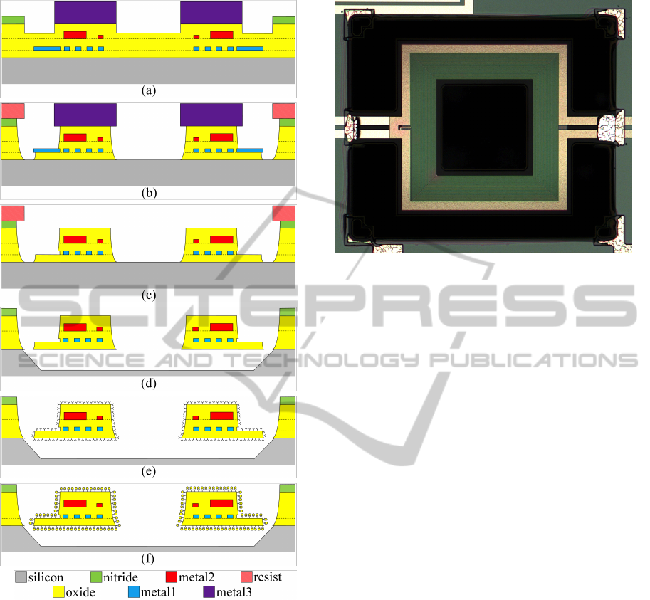
Figure 2: Sketch of the MEMS fabrication process (not to
scale). The single steps are described in the text.
inter-metal dielectric layers, while loops are fabri-
cated using the metal interconnection layers. A post-
processing sequence, designed to be CMOS compati-
ble, was used to release the microbalance.
The silicon chip section as received from the
foundry is shown in Fig.2a. The thick metal3 layer
(dark purple) is used as a mask to protect the res-
onator structure during the subsequent etch of the di-
electrics, basically silicon dioxide (yellow), while the
external structures (connection lines from and to the
loops, pads, etc.) are protected by a standard pho-
tolithographic resist (pink). The oxide is removed
in a buffered HF solution (Fig.2b) to reach the sili-
con substrate surface. At this point, the metal3 is not
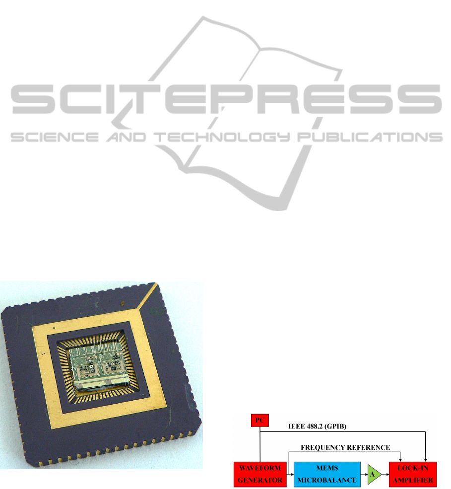
Figure 3: Optical microscope photograph of one the fab-
ricated resonators. The plate side length is 400 µm. The
driving loop (yellow outer border) is clearly visible. The
dark area corresponds to the cavity in the silicon substrate.
required anymore and is then removed in a wet etch
(Fig.2c). The resist is removed as well, and the release
phase can be performed. During the release, carried
out in a buffered tetra-methyl-ammonium hydroxide
(TMAH) solution at 85
◦
C, the silicon under the plate
is anisotropically etched along (100) planes, so that
the plate and springs are mechanically detached from
the substrate. The chemistry of the TMAH solution
is tuned to allow etch of the silicon while removing
both the oxide and the metal negligibly (Biswas et al.,
2006). Because of the anisotropy, a central hole is
required in the plate to allow complete release of the
structure (Fig.2d). At this point, the resonators appear
as in Fig.3. The overall dimensions of a resonator is
(depending on the specific type) in the range of a few
hundreds of micrometers.
Once the mechanical structure of the resonator is
ready, the sample is glued to the final, gold plated
ceramic package which will be used for electri-
cal characterization, and the silanization phase takes
place. Organo-functional silane deposition is com-
monly used as an intermediate step towards the cre-
ation of bioactive protein layers in biosensing appli-
cations. In this work, the silanization protocol devel-
oped in (Lenci et al., 2010) was tailored to suit the
needs of the specific application.
A preliminary cleaning of the sample in an ammo-
nia based solution (NH
4
OH(25%):H
2
O:H
2
O
2
(30%)
1:1:4 vol.) is performed. After 5
0
in the solution,
the sample is rinsed twice in deionized water (D.I.).
After this step, the resonator surface is terminated by
hydroxyl groups, which are required to allow covalent
bonding of the silane. While sulphuric acid-based so-
lutions (e.g. piranha) are most commonly used in the
FREQUENCY CHARACTERIZATION OF A MAGNETICALLY ACTUATED MEMS RESONANT BIOSENSOR
393
literature (Kim et al., 2008), they are not compatible
with exposed aluminium which is present in our sam-
ples at the external electric pads.
Immediately after rinsing, the sample is im-
mersed in an aqueous solution of 3-amino-propyl-
triethoxysilane (APTES) (0.05% vol.) for 5
0
, and
rinsed again in D.I. (Fig.2e). The sample then un-
dergoes a curing phase (Ballarin et al., 2008) by im-
mersion in acetone for 60
0
. During this phase, loosely
bound silane molecules or silane clusters are removed
and the overall quality of the silane layer improves.
At this point, the resonators are ready for charac-
terization. A single silicon chip contains up to four
resonators. The input and output inductors of each
resonator are bonded to the package gold contacts by
means of thin aluminum wires (Fig.4). A first fre-
quency response of the resonator is measured using
the procedure detailed in the next section. To elimi-
nate the influence of ambient humidity (a common in-
terferer for gravimetric sensor), the sample is heated
in oven at 120
◦
C for 30
0
and immediately moved to
a sealed aluminium box for the electrical character-
ization. The resonators are then loaded with an ad-
ditional mass to verify their behaviour as gravimetric
sensor.
The added mass is represented by gold NP’s which
are known to bind to the exposed amino groups of the
silane layer. A 25 µl drop of a 30nm gold NP colloid
(British Biocell International) is deposed on the chip
(Fig.2f). After 60
0
, the sample is rinsed in D.I., dried
in oven (30
0
at 120
◦
C), and the frequency response
of the resonators is then measured again. To ensure
that the NP anchoring is specific to the silane layer, a
Figure 4: Photograph of a sensor chip mounted in its ce-
ramic package. Each chip contains four working resonators.
The bonding wires connecting the chip pads to the package
are also visible. The package side is 2.5 cm.
reference sample underwent the same procedure with
the exclusion of the silanization steps.
The amount of added mass was estimated by
Scanning Electron Microscope (SEM) observation of
the resonator front surface at several different test
sites (6 to 8 for each resonator). The number of NP’s
at each site, 1µm ×1 µm in size, was counted and
averaged. The resultant added mass density µ
S
was
calculated by supposing a constant diameter of 30nm
for each NP, and then multiplied by the total resonator
surface to obtain an estimate of the total added mass.
No trace of NP’s was found on the reference sample.
3 CHARACTERIZATION SETUP
The instrumentation setup for electrical characteriza-
tion is sketched in Fig.5. The input current is provided
by a waveform generator. The output voltage signal is
pre-amplified (the voltage level is in the hundreds of
microvolt range) and then fed to a lock-in amplifier,
which measures the amplitude and phase relationship
between the input and the output signal. Both the
waveform generator and amplifier are remotely con-
trolled by a personal computer.
The external magnetic field is provided by two
permanent magnets. The field amplitude is around
70mT. Before each measurement session, the sam-
ple is dried in oven (see section 2.2) and placed in
a sealed aluminium box. At least two measurement
sessions are performed for each resonator: one after
silanization, and one after NP grafting.
For each session, four different frequency curves
are measured: the first, with a 20 kHz measure-
ment window centred at the theoretical resonance fre-
quency, obtained by FEM (Finite Element Method)
simulations, is used to identify the actual resonance
frequency peak. The other three measurements are
performed around the actual resonance frequency
with a 500 Hz window and a 5 Hz step. Each curve
requires between 10 and 30 minutes.
Moreover, as the magneto-mechanical coupling
coefficients (Γ
D
and Γ
S
of Eq.3) are proportional to
the magnetic field, a single response curve without
Figure 5: Schematic representation of the experimental
setup for electrical characterization.
BIODEVICES 2011 - International Conference on Biomedical Electronics and Devices
394

Table 1: Experimentally extracted parameters for two different resonators.
MB108
f
0
σ
f
0
f
D
σ
f
D
Q σ
Q
µ
S
σ
µ
S
S
[Hz] [Hz] [Hz] [Hz] [kg/m
2
] [kg/m
2
] [m
2
/kg]
200×200 94581 2.5 94291 2.5 287 1.26 3.67·10
−5
0.57·10
−5
−79.59
400×400 31749 1.0 31612 0.6 157 5.67 3.86·10
−5
1.31·10
−5
−117.27
magnets (and thus with Γ
D
= Γ
S
= 0) is also per-
formed on each resonator to extract the value of the
mutual inductive coupling coefficient M.
The purely mechanical response (i.e. the first term
in the RHS of Eq.3) is then extracted by subtraction of
the mutual inductance term from the actual measured
data. The obtained data points are then numerically
fitted against the analytical expression of the mechan-
ical response to extract the most relevant mechani-
cal parameters, most importantly (from the applica-
tion point of view) the resonance frequency f and the
quality factor Q. For each resonator, their values are
averaged over the three measurements. Typical mea-
sured response curves are presented in Fig.6, where
the effect of the added mass on the resonance fre-
quency is also shown.
4 DISCUSSION AND
CONCLUSIONS
Typical extracted parameters from two different res-
onator types, fabricated on the same chip, are sum-
marized in Table 1. The MB108-400 resonator is
the device shown in Fig.3; the MB108-200 resonator
is a similar device, but with a smaller central plate
(200µm ×200 µm) and comparatively longer suspen-
sion springs. For each parameter, both the averaged
value (over three measures) and its standard deviation
(σ
∗
) are shown.
The initial resonance frequency f
0
was measured
immediately after silanization, and its value is af-
fected by very little error. The resonance frequency
after NP exposure, f
D
is consistently lower than the
initial frequency, and corresponds to a frequency shift
of a few hundred hertz (or 0.75% and 0.30% for the
two resonators, respectively). While the resonance
frequency tends to drift to higher values after a few
days on ambient storage (most likely because of ad-
sorption of ambient moisture), a drying step (30
0
at
120
◦
C) recovers its original value almost completely.
The frequency shifts must be compared to the
measured values of the added mass density µ
S
to ob-
tain an estimate of the sensor sensitivity. Given the
different area of the two devices, a sensitivity param-
eter allowing a fair comparison can be defined as (Jan-
shoff et al., 2000):
S =
f
D
− f
0
f
0
µ
S
[m
2
kg
−1
] (4)
The measured values for our resonators are around
79.6 and 117.3m
2
kg
−1
for the two devices (Table 1,
last column). These values compare favourably to
the typical values for macroscopic QCM’s (about
1m
2
kg
−1
in (Janshoff et al., 2000)), but also to other
MEMS resonant sensors: (Zuniga et al., 2009), for
example, claims about 60 m
2
kg
−1
. Compare also, for
a review, (Shen et al., 2010).
If the resonator plate thickness and density are
known, Eq.2 can be used to extract a theoretical value
of the mass density µ
S,T
from experimental frequency
shift data. If this analysis is carried out for our
devices, the theoretical mass density is consistently
higher than the measured one (by a factor of two or
more in some cases), with a correspondingly higher
value of the actual sensitivity S. Separate FEM anal-
ysis confirms the trend implied by the simplified an-
alytical model used to obtain Eq.2, so that this dis-
crepancy cannot attributed to oversimplification in the
mechanical model. Several other factors might come
into play in this case. Among them, the effect of the
NP adhesion on the residual (usually compressive)
stresses of the plate oxide film (which are certainly
present due to fabrication issues and were neglected in
this analysis) and on the overall stiffness of the mem-
Figure 6: Frequency response of the resonator of Fig.3, be-
fore (blue) and after (red) NP grafting. Actual data are in-
dicated by the dots, while the lines are fitted curves. The
contribution of the mutual inductance is not subtracted yet
(see text).
FREQUENCY CHARACTERIZATION OF A MAGNETICALLY ACTUATED MEMS RESONANT BIOSENSOR
395

brane (in particular in the torsional beams).
In conclusion, we demonstrated the operation
of a magnetically actuated MEMS resonator with
electrical input and output as a sensitive mass sen-
sor. The measured sensitivities can be compared
favourably to standard QCM’s and other imple-
mented MEMS microbalances. Moreover, a MEMS-
compatible silanization protocol for the resonator ac-
tive surface was developed as well. Such a silane
layer can be used as a precursor to the fabrication of a
bioactive layer to transform the device in a complete
resonant biosensor.
ACKNOWLEDGEMENTS
This work was partly financed under a PRIN 2008
grant by the Italian Ministry for University and Re-
search.
REFERENCES
Ballarin, B., Cassani, M., Scavetta, E., and Tonelli, D.
(2008). Self-assembled gold nanoparticles modified
ito electrodes: The monolayer binder molecule effect.
Electrochim. Acta, 53:8034–8044.
Biswas, K., Das, S., Maurya, D., Kal, S., and Lahiri, S.
(2006). Bulk micromachining of silicon in tmah-based
etchants for aluminum passivation and smooth sur-
face. Microel. J., 37:321–327.
Diegoli, S., Mendes, P., Baguley, E., Leigh, S., Iqbal,
P., Diaz, Y. G., Begum, S., Critchley, K., Ham-
mond, G., Evans, S., Attwood, D., Jones, I., and
Preece, J. (2006). ph-dependent gold nanoparticle
self-organization on functionalized si/sio2 surfaces.
Journal of Experimental Nanoscience, 3:333–353.
Janshoff, A., Galla, H., and Steinem, C. (2000). Piezoelec-
tric mass-sensing devices as biosensors - an alternative
to optical biosensors? Angew. Chem. Int., 39:4004–
4032.
Kim, J., Seidler, P., Fill, C., and Wan, S. (2008). Investiga-
tions of the effect of curing conditions on the structure
and stability of amino-functionalized organic films on
silicon substrates by fourier transform infrared spec-
troscopy, ellipsometry, and fluorescence microscopy.
Surf. Sci., 602:3323–3330.
Lenci, S., Tedeschi, L., Domenici, C., Lande, C., Nan-
nini, A., Pennelli, G., Pieri, F., and Severi, S.
(2010). Protein patterning on polycrystalline silicon–
germanium via standard uv lithography for biomems
applications. Materials Science and Engineering C,
doi:10.1016/j.msec.2010.07.002.
Maboudian, R. and Howe, T. (1997). Critical review: ad-
hesion in surface micromechanical structures. J. Vac.
Sci. Technol. B., 15:1–20.
Paci, D., Pieri, F., Toscano, P., and Nannini, A. (2008). A
cmos-compatible, magnetically actuated resonator for
mass sensing applications. Sensors and Actuators B,
129:10–17.
Shen, W., Mathison, L., Petrenko, V., and Chin, B. (2010).
A pulse system for spectrum analysis of magnetoelas-
tic biosensors. Appl. Phys. Lett., 96:163502.
Sone, H., Okano, H., and Hosaka, S. (2004). Picogram
mass sensor using piezoresistive cantilever for biosen-
sor. Jpn. J. Appl. Phys., 43:4663–4666.
Teva, J., Abadala, G., Torresa, F., Verda, J., P
´
erez-Murano,
F., and Barniola, N. (2006). A femtogram resolution
mass sensor platform, based on soi electrostatically
driven resonant cantilever. part i: Electromechanical
model and parameter extraction. Ultramicroscopy,
106:800–807.
Tilmans, H. (1996). Equivalent circuit representation of
electromechanical transducers: I. lumped-parameter
systems. J. Micromech. Microeng, 6:157–176.
Zuniga, C., Rinaldi, M., Khamis, S., Johnson, A., and Pi-
azza, G. (2009). Nanoenabled microelectromechani-
cal sensor for volatile organic chemical detection. Ap-
plied Physics Letters, 94:223122.
BIODEVICES 2011 - International Conference on Biomedical Electronics and Devices
396
