
PORTABLE DOSIMETER WITH MOSFET SENSOR FOR
RADIOTHERAPY MONITORING
M. A. Carvajal, J. Banqueri, A. J. Palma
Departament of Electronics and Computer Technology, University of Granada, ETSIIT, CITIC-UGR, Granada, Spain
A. M. Lallena
Department of Molecular, Nuclear and Atomic Physics, University of Granda, Granada, Spain
D. Guirado, M. Vilches
Department of Radiophysics, University Hospital San Cecilio, Granada, Spain
Keywords: Radiation sensor, Dosimeter, MOSFET, Radiotherapy, Portable instrument.
Abstract: A portable dosimeter based on unbiased MOSFET sensor is presented. Its main characteristics are an
extended linearity range and a notable thermal drift reduction using a unique p-channel MOSFET (pMOS)
unbiased during the irradiation period, allowing the location of the sensor without wires for patient comfort
and easy-to-use. Both features have been obtained with novel procedures of dose reading and signal
processing applied to low-cost commercial pMOS. In this work, a full description of the electronics of the
dosimetry system and the signal processing techniques are drawn. The system has been tested with photons
from
60
Co and the complete technical specifications have been obtained. Among them, we can emphasize: i)
dose sensitivity of around 25 mV/Gy; ii) linearity range of more than 50 Gy, with intermediate calibration
each 15 Gy, for each sensor; iii) thermal drift below 3 mGy/ºC; iv) resolution below 1cGy; and v) total
uncertainty of ± 9 mGy in the temperature range from 19 ºC to 36 ºC . We believe that the proposed
dosimeter could be a novel and feasible low-cost alternative to previous commercial dosimetry systems for
radiotherapy monitoring in clinical applications.
1 INTRODUCTION
In the last few decades, MOSFETs (Metal-Oxide-
Semiconductor Field Effect Transistors) have been
used widely as dosimeters due to their small size,
immediate and non-destructive readout, low power
consumption, easy calibration, and reasonable
sensitivity and reproducibility (Holmes-Siedle and
Adams, 1986; Hughes et al., 1988; Soubra et al.,
1994). These desirable characteristics have
promoted the use of this device in different fields
such as spacecraft, radiotherapy, skin dosimetry, and
clinical monitoring (Buehler et al., 1993;
Sarrabayrouse and Siskos, 1998; Benson et al.,
2000; Rosenfeld, 2002; Bloemen et al., 2003; Haran
et al., 2004; Best et al., 2005; Kwan et al., 2008).
Ionizing radiation produces electron-hole pairs in
the MOS structure that are separated by an electric
field established in the gate oxide and near the
silicon-gate oxide interface. During irradiation, the
structure can be configured without an external
voltage (unbiased mode), or the electric field can be
made larger by applying an external voltage between
the gate and the bulk of the device (biased mode).
The charge accumulated in the structure produces
changes in the electrical parameters that can be
measured experimentally, usually after irradiation,
during the so-called readout period. The electrical
parameter of the MOS transistors most commonly
used as a dosimetric parameter (i.e., the parameter
from which the dose is extracted) is the threshold
voltage (V
T
), which is the gate-source voltage
necessary to induce channel inversion between the
source and drain terminals. Many works show an
approximately linear dependence between the V
T
shift and the absorbed dose in the oxide for p-
23
Carvajal M., Banqueri J., Palma A., Lallena A., Vilches M. and Guirado D..
PORTABLE DOSIMETER WITH MOSFET SENSOR FOR RADIOTHERAPY MONITORING.
DOI: 10.5220/0003128100230029
In Proceedings of the International Conference on Biomedical Electronics and Devices (BIODEVICES-2011), pages 23-29
ISBN: 978-989-8425-37-9
Copyright
c
2011 SCITEPRESS (Science and Technology Publications, Lda.)

channel MOSFETs (pMOS) (Sarrabayrouse and
Siskos, 1998; Ma and Dressendorfer, 1989; Hughes
et al., 1988).
During readout, the V
T
determination can be
carried out by extracting the complete current-
voltage characteristic curve of the device (Asensio et
al., 2006) or by using simpler methods based on
constant current measurements. Basically, the
measurement methods consist in recording the drain-
source voltage while the transistor is being polarized
with a constant drain current, before and after
irradiation. Under this configuration, the source-
drain voltage shifts equals, approximately, the
increase in V
T
(Sarrabayrouse and Siskos, 1998;
Asensio et al., 2006; Carvajal et al., 2010).
Most commercial dosimetric systems based on
MOSFETs, measure increases in drain-source
voltage at constant drain current
(Thomson&Nielsen, 1991; Halvorsen, 2005).
Usually, in order to minimize thermal drift, the drain
current selected is the Zero Temperature Coefficient,
I
ZTC
, because the drain-source voltage is invariant
when temperature increases. The dosimetric
parameter used by one of the commercial dosimetric
systems is the difference of the increase in drain-
source voltages of two transistors under different
polarizations. With this arrangement, a wide linear
range and thermal compensation are achieved in the
biased mode (Thomson&Nielsen, 1991). There is
another commercial system based on transistors in
the unbiased mode, but the linear range is up to 5 Gy
and its use is limited to only one irradiation session
(Halvorsen 2005; Sicel Technologies, 2005, Best et
al., 2005).
In previous works (Asensio et al. 2006, Carvajal
et al., 2010; Carvajal et al., 2010b), we showed the
feasibility of using a general-purpose low-cost
pMOS as dosimeter, irradiated in unbiased mode,
with a significant increase in linear range compared
with similar systems and reduced thermal drift.
These improvements are based on gate-source
voltage measurements at three different drain
currents during readout instead of the usual method
with a single polarization current.
Although this work has focussed on the pMOS
dosimeter, it is important to point out that the
proposed methodology could be applied to other
sensors based on MOSFET, such as CHEMFET or
ISFET, where the magnitude under study is
extracted from the threshold voltage. In these cases
(Fraden, 1996), the threshold voltage is also
measured at constant drain current.
In the following section, a complete
measurement system description is carried out,
including the measurement algoritmh and an
explanation of the electronic system. After this, the
experimental setup used in our experiments is
described. We report experimental results of the
dosimetric characterization of the dosimeter
presented here and its technical specifications are
shown. Finally, the main conclusions are drawn.
2 DOSIMETER DESCRIPTION
In this section, a detailed description of the
measurement algorithm and the electronic design of
the dosimeter will be carried out.
2.1 Measurement Algorithm
First, the theoretical background of the measurement
process, developed in previous works, will be
resumed (Carvajal et al., 2010; Carvajal et al.,
2010b). This is the basis on which the electronic
design relies on. The operation method of the dose
measuring of the presented dosimeter is the same of
most previous devices based on MOSFET sensors.
Before the sensor irradiation, an electronic reader
unit measures the electrical characteristics of the
sensor; this is usually named as sensor zeroing (first
readout period). Then, sensor is irradiated
(irradiation period) and, finally, another readout
process is carried out to measure the MOSFET
electrical characteristics shifts caused by the
irradiation. Here during the irradiation period, we
have configured the sensor in the unbiased mode, i.e.
short-circuiting all its terminals and without
polarization, obtaining a sensor without wires in this
period.
During the dose readout under constant drain
current bias, the gate and the drain terminals of the
MOSFET are usually short-circuited and grounded,
and the bulk and the source are also inter-connected
(Sarrabayrouse and Siskos, 1998; Best et al., 2005).
In this configuration, the transistor operates in the
saturation region, where
SD
VI − can be modelled
for pMOS (Sze, 1981):
()
2
2
TSD
VV
β
I −=
(1)
where the drain current,
D
I , depends on the source
voltage,
S
V , the threshold voltage,
T
V , and the
β
parameter,
L
W
C
oxp
μβ
=
, where
p
μ
is the carrier
mobility in the channel,
ox
C is the oxide
BIODEVICES 2011 - International Conference on Biomedical Electronics and Devices
24

capacitance, and W and L are the channel width and
length respectively.
From Equation (1), the threshold voltage can be
calculated before (pre) and after (post) irradiation:
pre
D
pre
S
pre
t
IVV
β
1
2−=
(2a)
post
D
post
S
post
t
IVV
β
1
2−=
(2b)
Therefore, the voltage threshold shift can be
calculated as follows:
⎟
⎟
⎠
⎞
⎜
⎜
⎝
⎛
−−Δ=Δ
prepost
DSt
IVV
ββ
11
2
(3)
If the increase in the source voltage is measured
at two different currents, we can write:
⎟
⎟
⎠
⎞
⎜
⎜
⎝
⎛
−−Δ=Δ
prepost
DSt
IVV
ββ
11
2
11
(4a)
and
⎟
⎟
⎠
⎞
⎜
⎜
⎝
⎛
−−Δ=Δ
prepost
DSt
IVV
ββ
11
2
22
(4b)
where
Si
VΔ is the source voltage shift measured at
constant current
Di
I . Using (4a) and (4b), the
threshold voltage shift can be calculated as (Carvajal
et al, 2010):
1
2
12
1
1
D
D
SS
St
I
I
VV
VV
−
Δ−Δ
+Δ=Δ
(5)
With Equation (5), the threshold voltage shifts can
be calculated exactly from the source voltage shifts
instead of approximated to the source voltage, as has
been done until now.
According to equation (5), threshold voltage
shifts can be found from voltage increases measured
with two different currents, separating the
contribution to the source-voltage shifts due to
β
Δ
and
T
VΔ and resulting in an extended linear range
for the sensor (Carvajal et al, 2010). Moreover, if a
third current is applied, a thermal-compensation
method and the extension of the linear range can be
used simultaneously. Two currents are needed to
evaluate equation (5),
1D
I and
2D
I , and an
additional current,
C
I , is required for the thermal
compensation of the source voltage shifts measured
at
1D
I and
2D
I (Carvajal et al., 2010b):
()
()
,
,
2
2
22
0
2
1
1
11
0
1
CD
ZTCD
SSCSS
CD
ZTCD
SSCSS
II
II
VVVV
II
II
VVVV
−
−
Δ−Δ+Δ=Δ
−
−
Δ−Δ+Δ=Δ
(6)
where I
ZTC
is the current with minimal thermal
coefficient of the threshold voltage. According to
equation (5), we have:
1
2
0
1
0
2
0
1
0
1
D
D
SS
ST
I
I
VV
VV
−
Δ−Δ
+Δ=Δ
(7)
Evaluating equations (6) and (7) sequentially
allows both the thermal compensation and the
linearity improvement methods to be taken into
account, and provides the thermally compensated
threshold voltage shifts from the source-voltage
increments measured at three different currents. One
need only know the value of
ZTC
I and the intensities
used to polarize the transistor during readout. If one
of the currents,
1D
I or
2D
I , is equal to
ZTC
I ,
equation (7) is simplified. For example,
if
ZTCD
II
=
2
, the source voltage shifts at
2D
I are
thermally compensated, and all that is left is to
evaluate equation (7) for
1S
V
Δ
and
C
VΔ in order to
find
0
1S
VΔ
.
Moreover, polarizing with pulsed instead of
constant currents, most of the 1/f noise is avoided,
obtaining a higher signal-to noise ratio of the
measurement (Carvajal et al, 2010).
2.2 Measurement Electronic System
The dosimetric system consists of a read-out unit
and a set of sensor modules.
The sensor module is based on the commercial
general-purpose pMOS 3N163, which is located on
a printed circuit board (PCB). During irradiation and
storage periods, all the terminal of the MOSFET
must be short-circuited together. In previous works,
we used a power supply jack for this purpose, but
resulted in a sensor module too thick that could
produce radiation shadow areas. For minimizing this
effect in the radiation field, the jack was replaced by
an n-channel JFET (see Figure 1), with SMD case
(surface-mounted-device). We used the MMBF4391
of NXP Semiconductor (Netherland), with a cut off
PORTABLE DOSIMETER WITH MOSFET SENSOR FOR RADIOTHERAPY MONITORING
25

voltage of -10V and resistance of 30 Ω, and it was
welded in the bottom layer of the PCB. This
transistor is normally on and maintains connected
the source and bulk terminals with the drain and
gate. This connection must be opened for zeroing
and voltages shifts measurements. Therefore the
read-out unit has to provide the adequate source-gate
voltage for JFET cut off during the readout process.
When the sensor module is removed from the read-
out unit, the gate capacitance of the JFET is
discharge through a resistor, R
G
. Therefore, all the
MOSFET terminals are connected again.
S
G
D
B
pMOSFET
JFET
R
G
Figure 1: Sensor module schematic.
The readout unit is an electronic system
controlled by a microcontroller (Figure 3). We used
the PIC-16F877 of the mid-range family of
Microchip (USA) due mainly to its low power
consumption, its 10 bits analog-to-digital converter
(ADC), four independent input/outputs ports and
I2C and UART ports. An EEPROM memory is
included in order to storage different parameters of
each sensor module. One reader unit can support up
to 256 different sensor modules. Each sensor module
must be identified for zeroing and for dose
measurements.
Figure 2: Reader and sensor module.
Figure 3 shows the block diagram of the analog
circuitry and the microcontroller. The analog
subsystem consists mainly, in a programmable
current source, an instrumental amplifier and a
digital to analog converter (DAC). During the
measurements process of the sensor module, the
JFET is cut off, and the programmable source
polarizes the MOSFET at different currents, being
measured the source voltages by the read-out unit.
For zeroing, the microcontroller calculates the DAC
output voltage necessary to reduce the instrumental
amplifier output down to tens of milivolts. The
digitalized source voltages, and the DAC words are
storage in the EEPROM, mapped in EEPROM
depends on the sensor module identification number,
ID. At least, two minutes after the irradiation ends,
the dose measurement can be carried out. The sensor
ID is introduced in the keypad, and DAC words are
restored for each polarization currents. Then, the
source voltage source shift can be calculated. The
calibration parameters are read from the EEPROM,
and the dose are calculated. Finally the results are
shown on the display or can be downloaded to the
computer.
V
DD
Programable
current
source
V
S
I
D
Timer
555
pMOSFET
BJT
G
S
D
B
Microcontroller
V
S
aconditionating
circuit
A.I. A/D
DAC
A/D
Figure 3: Block diagram of the analog circuitry.
In addition, during the readout process, the
pMOS current is switched in order to reduce the 1/f
noise and to increase the linearity as Carvajal et al.
2010 shown in a laboratory setup. The collector of a
bipolar transistor, the BC547 of NXP
Semiconductors (Netherland), is connected to the
source of the MOSFET and the emitter is grounded.
When the bipolar transistor is activated, the current
drains by the BJT, forcing the source voltage of
pMOS to zero. But, when the BJT is deactivated, the
current crosses the pMOS transistor, and then the
source measurement are carried out. The pulse
signal was generated with a timer 555. The PWM
module of the microcontroller was not used because
the PIC was in sleep mode during A/D
measurements to reduce the noise produced by the
crystal oscillator of the PIC.
The readout unit can be configured by a 4x4
keypad or by computer via the USB port. The results
BIODEVICES 2011 - International Conference on Biomedical Electronics and Devices
26

can be shown on the LCD screen and/or be sent to
the PC (Figure 2).
3 EXPERIMENTAL RESULTS
3.1 Experimental Setup
For the evaluation of the presented dosimetry
system, a total of eight sensor modules were
irradiated with an AECL Theratron 780 located at
the University Hospital of San Cecilio in Granada
(Spain). This is a teletherapy unit with a
60
Co source.
All the irradiations were carried out with all four
transistor terminals connected to each other, hence
without bias voltage, in the ‘unbiased’ mode. The
transistors were irradiated with a 40 x 40 cm
2
field
and were placed at the isocentre, at 80 cm from the
source. Five transistors were used to study the
linearity and measurement range, two for the long-
term fading and the last one for short-term fading.
According to a previous work, the three
polarization currents included in the dosimeter setup
and applied to the sensor during the readout periods
were I
D1
= 30 µA, I
D2
= I
ZTC
= 225 µA and I
C
= 120
µA
. With these current values a thermal drift below
3 mGy/ºC has been obtained (Carvajal et al, 2010b).
Moreover, for sensor equalization, an initial pre-
irradiation of 30 Gy was necessary.
3.2 Dosimetric Evaluation
In order to evaluate the dosimetric behaviour of the
dosimeter, the post-irradiation fading and the
linearity range. All these results have been obtained
with equations 6 and 7 included in the signal
processing.
3.2.1 Post-irradiation Fading
The reordering of the MOSFET charge after the
irradiation produces shifts in the dosimetric
parameter, i.e. the voltage threshold, which could
false the dose reading. This effect is inherent to the
transduction principle (measurement of the dose by
the charge creation) and very difficulty avoidable.
However, what you can do is to characterize it to
keep it under control. This has been done with our
dosimeter, measuring the short-term fading and the
log-term fading to give a time period when both are
negligible.
In Figure 4, the short-term post-irradiation
fading is shown for several accumulated dose. In this
figure, the threshold voltage transient (in arbitrary
units) is measured as a function of time.
260
280
300
320
340
360
380
400
0 50 100 150 200 250 300
t(s)
n_ADC
3Gy
9Gy
12Gy
15Gy
18Gy
21Gy
24Gy
27Gy
30Gy
Figure 4: Short-term post-irradiation fading.
From Figure 4, we can observe a measurable
transient in the first 60 s and that for long times it is
negligible even at higher accumulated dose. The
long-term post-irradiation fading was measured
every 12 hours, for two sensors with accumulated
dose of 27 Gy in 3 Gy sessions. The threshold
voltage long-term transients are shown in Figure 5.
y = 9.33E+01e
-1.62E-06x
R
2
= 9.97E-01
y = 8.90E+01e
-1.77E-06x
R
2
= 9.97E-01
0
10
20
30
40
50
60
70
80
90
100
0.0E+00 2.0E+05 4.0E+05 6.0E+05
t (s)
Δ
Vs (mV)
6
7
Figure 5: Long-term post-irradiation fading.
From Figure 5, a time constant of around one
week was obtained with an exponential fit, in
agreement with reported results (Ma and
Dressendorfer, 1989). Thus, this dosimeter obtains
dose measurements without fading interference at
times longer than 60 s and shorter than a few hours
after the sensor irradiation. Therefore, we have
stated a delay for the measurement between 2 and 3
minutes.
3.2.2 Linearity
One of the disadvantages of using MOSFET sensors
in the unbiased mode is the reduced linearity range
(Sarrabayrouse and Siskos, 1998). With the readout
procedure and the developed instrumentation, this
characteristic has been notably improved. Session
sensitivities (normalized voltage threshold shift,
mV/Gy, per irradiation) are depicted in Figure 6. In
Figure 7, the accumulate threshold voltage shifts as a
function of the dose up to 52 Gy are shown for five
PORTABLE DOSIMETER WITH MOSFET SENSOR FOR RADIOTHERAPY MONITORING
27
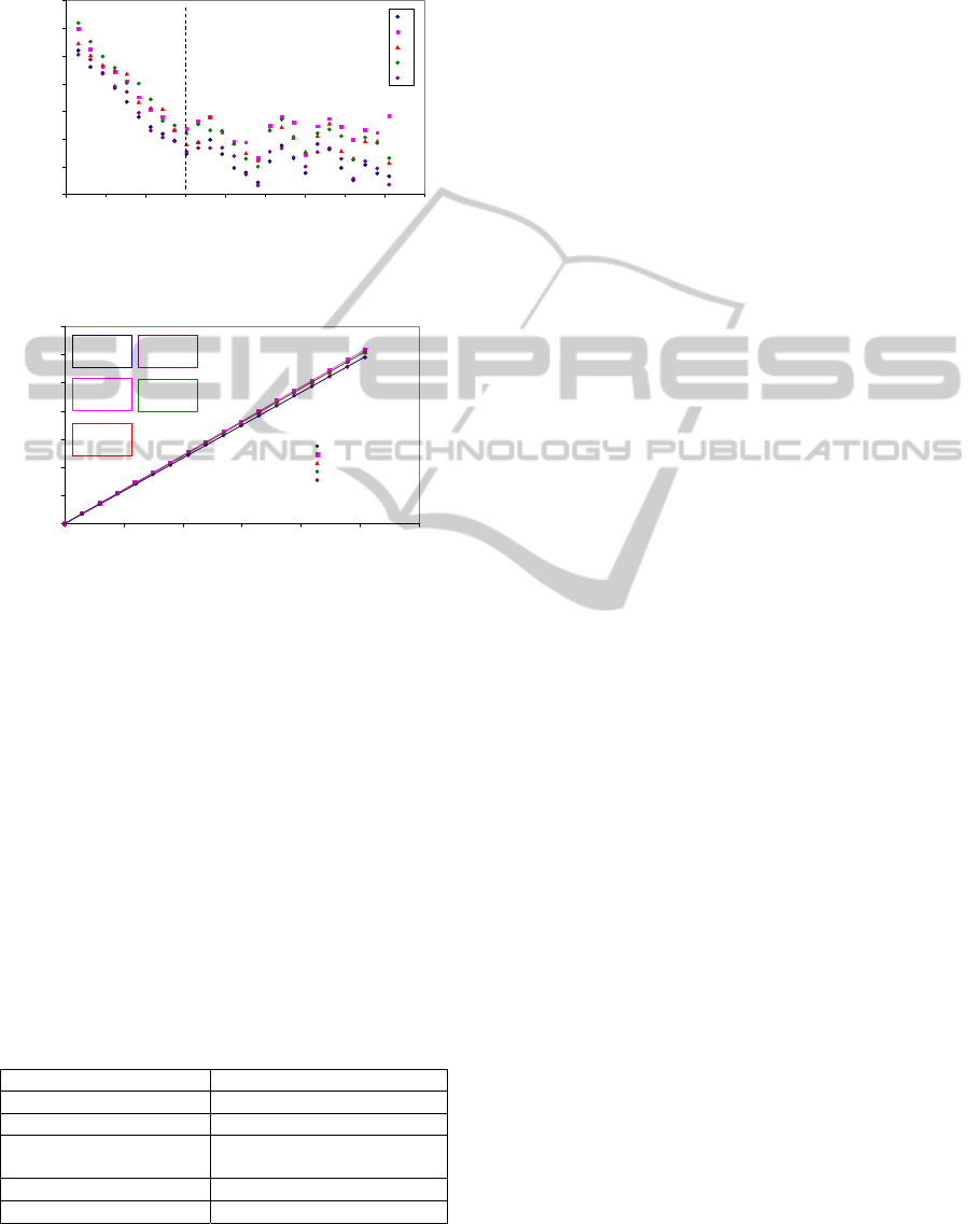
sensors, where the first 30 Gy have been subtracted
and used as pre-irradiation dose for sensor
equalization and to improve the sensitivity stability
22
23
24
25
26
27
28
29
0 20406080
D (Gy)
Sen (mV/Gy)
1
2
3
4
5
Previous
irradiations
Dose
measurements
Figure 6: Irradiation session sensitivities versus
accumulated dose.
y = 0.0233x
R
2
= 1.0000
y = 0.0240x
R
2
= 1.0000
y = 0.0240x
R
2
= 1.0000
y = 0.0243x
R
2
= 1.0000
y = 0.0232x
R
2
= 1.0000
0.0
0.2
0.4
0.6
0.8
1.0
1.2
1.4
0 102030405060
D-Dpre (Gy)
Δ
V
t
(V)
1
2
3
4
5
Li l (5)
Figure 7: Accumulated threshold voltages shifts versus
accumulated dose.
From figures 6 and 7, several remarks can be
extracted:
i. A pre-irradiation of 30 Gy is necessary for
equalization.
ii. After pre-irradiation, a good linearity is observed
iii. Intervals of accumulated dose of 15 Gy produce
linearity errors below 5%
iv. User recalibration every 15 Gy are needed to sure
good accuracy for extended linear range up to 52 Gy
with a unique sensor.
3.2.3 Technical Specification
In Table 1, the main technical specifications of the
presented dosimeter are resumed:
Table 1: Dosimeter technical specifications.
Temperature range 10 – 40 ºC
Resolution 1 cGy
Accuracy ± 3 %
Linear range
15 Gy
> 80 Gy
*
Thermal drift < 3mGy/ºC
Delay after irradiation 2 – 3 minutes
* with recalibrations every 15 Gy.
4 CONCLUSIONS
A novel dosimeter based on MOSFET sensor is
presented, suitable for radiotherapy monitoring. In
the same instrument, main advantages of previous
commercial equipment have been joined such us low
thermal and fading interference, enough resolution
and accuracy for clinical usage, extended linear
range and portable reader with wireless sensors.
Moreover, these features have been obtained with a
low-cost commercial MOSFET instead of expensive
and dedicated radiation sensor based on MOS
technology.
Regarding with future works, preliminary results
with LINAC irradiations (6 and 18 MV) are quite
promising. Build-up layer needs to be increased as
energy photons increases but general performance is
similar to the presented results for Cobalt source.
ACKNOWLEDGEMENTS
This work has been funded by the Ministerio de
Educación y Ciencia, Dirección General de
Enseñanza Superior (Spain) (Projects CTQ2009-
14428-CO2-01, CTQ2009-14428-CO2-02), from the
Junta de Andalucía (Projects P09-FQM-5341, P08-
FQM-3535) and from the Ministerio de Ciencia e
Innovación (Project PS-300000-2009-5).
REFERENCES
Asensio L J, Carvajal M A , López-Villanueva J A, M.
Vilches, A. M. Lallena and A. J. Palma, 2006
Evaluation of a low-cost commercial MOSFET as
radiation dosimeter Sensors and Actuators A 125 288-
295,.
Benson C, Joyce M J, O’Connell B and Silvie J 2000
Neutron Detection at the Extremes of Sensitivity in the
Cosmic Environment IEEE Trans Nucl. Sci. 6 2417-
2422.
Best S, Ralson A and Suchowerska N 2005 Clinical
Application of the OneDose
TM
Patient Dosimetry
System for total body irradiation Phys. Med. Biol. 50
5909-5919.
Bloemen E, Bois W, P. Visser P, Bruinvis I, Jalink D,
Hermans J and Lambin P 2003 Clinical dosimetry
with MOSFET dosimeters to determinate the dose
along the field junction in a split beam technique
Radiother. Oncol. 67 (2003) 351-357.
Buehler M G, Blaes B R, Soli G A and Tardio G R 1993
On Chip p-MOSFET Dosimetry IEEE Trans. Nucl.
Sci. 40 1442-1449.
BIODEVICES 2011 - International Conference on Biomedical Electronics and Devices
28

Carvajal M A, Vilches M, Guirado D, Lallena A M,
Banqueri J and Palma A J, 2010 Readout techniques
for linearity and resolution improvements in MOSFET
dosimeters Sensors and Actuators A 157 178–184.
Carvajal M A, Martínez-Olmos A, Morales D P,
López-Villanueva J A, Lallena A M and Palma A J,
2010 Thermal Drift Reduction With Multiple Current
Polarization For MOSFET Dosimeters send for
publication to Phys. Med. Biol.
Fraden J, 1996 Handbook of modern sensor. Physics,
design and application, 2
nd
Edition (New York:
Springer Science+Biseness Media).
Halvorsen P. H. 2005. Dosimetric evaluation of a new
design MOSFET in vivo dosimeter, Med. Phys. 32
110-117.
Haran A, Jaksic A, Refaeli N, Eliyahu A, David D and
Barak J 2004 Temperature Effects and Long Term
Fading of Implanted and Unimplanted Gate Oxide
RADFETs, IEEE Trans. Nucl. Sci. 5 2917-2921.
Holmes-Siedle A and Adams L 1986 RADFET: A review
of the use of metal-oxide-silicon devices as integrating
dosimeters Radiat. Phys. Chem. 28 235-244.
Hughes R C, Huffman D, Snelling J V, Zipperian J E,
Ricco A J and Kelsy A 1988 Miniature Radiation
Dosimeter for In-Vivo Radiation Measurements, Int. J.
Radiat. Oncol. Biol. Phys. 14 963-967.
Kwan I S, Rosenfeld A B, Qia Z Y, Wilkinson D, Lerch M
L F, Cutajar D L, Safavi-Naeni M, Butson M, Bucci J
A, Chin Y and Perevertaylo V L 2008 Skin dosimetry
with newMOSFET detectors Radiation Measurements
43 929 – 932.
Ma T P and Dressendorfer P V 1989 Ionizing Radiation
Effects In MOS Devices and Circuits (New York: John
Wiley & Sons).
Rosenfeld A B 2002 MOSFET Dosimetry on Modern
Radiation Oncology Modalities, Radiat. Prot. Dosim.
101 393-398.
Sarrabayrouse G and Siskos S 1998 Radiation Dose
Measurement using MOSFETs, IEEE Instrum. Meas.
Mag. 1 26-34.
Soubra M, Cygler J and Mackay G 1994 Evaluation of a
dual bias metal oxide-silicon semiconductor field
effect transistor detector as radiation dosimeter, Med.
Phys. 21 (1994) 567-572.
Sicel Technologies 2005 OneDose User´s Manual,
Pre-production draft version, rev. P01, (Morrisville:
Sicel Technologies Inc.).
Sze S M 1981 Physics of Semiconductor Devices, 2
nd
edition. (New York: John Wiley & Sons)
Thomson & Nielsen 1991 Direct reading dosimeter
European Patent Office EP 0471957A2, (02/07/1991).
PORTABLE DOSIMETER WITH MOSFET SENSOR FOR RADIOTHERAPY MONITORING
29
