
TOWARDS ASYNCHRONOUS SIGNAL PROCESSING
Dariusz Kościelnik and Marek Miśkowicz
Department of Electronics, AGH University of Science and Technology, al. Mickiewicza 30, Cracow, Poland
Keywords: Asynchronous circuits, Analog-to-digital converters, Asynchronous Sigma-Delta modulation.
Abstract: A challenging problem of today’s ADC design is a development of low voltage, low power and possibly
high performance converters. The ever growing demand for decreasing the supply voltage of semiconductor
devices due to scaling the feature size of VLSI technology has pushed the design of analog integrated circuit
to its limits. The same problem concerns the analog-to-digital converters since lowering supply voltage
results in a reduction of a voltage increment corresponding to the least significant bit (LSB) in signal
amplitude quantization. In the paper, an important alternative to conventional ADCs is presented. To
overcome problems with decreasing accuracy of amplitude quantization, a new class of asynchronous ADCs
is discussed where the mapping of an analog signal into time domain rather than into amplitude domain is
used. The asynchronous ADCs are not controlled by any global clock but self-timed. The local reference
clock is used only to quantize time intervals that represent the converted signal amplitude. The design of
asynchronous Sigma-Delta analog-to-digital converter (ASD-ADC) with serial output interface is discussed
in details. The ASD-ADC together with the loss-free asynchronous analog signal recovery method
developed recently provides possibility to establish the asynchronous digital signal processing chain.
1 INTRODUCTION
The ever growing demand for extending digital
functionality on a single chip results in scaling the
feature size of VLSI technology in order to increase
the integration density of semiconductor devices.
Scaling the CMOS transistor dimensions into
nanoscale (<100 nm) enables faster operation of
circuits on the one hand, but needs decreasing the
supply voltage of devices to maintain reliable
operation on the other. As a result of this, a design of
analog and mixed signal systems has to cope with an
ever increasingly challenging technological
environment. For example, with the operating
voltage of 1V, the output signal swing is only 0.3V,
which is unacceptably low signal swing for many
applications (Matsuzawa, 2007).
In the context of analog-to-digital converters
(ADCs), the technology
scaling increases the
maximum conversion rate, but unfortunately
decreases at the same time
the signal-to-noise ratio
(SNR). The latter is caused simply by a reduction of
voltage increment corresponding to the least
significant bit (LSB) in a signal amplitude
quantization. This is currently the most serious
problem of a classical ADC design that will be even
more critical in future with further scaling of CMOS
process technology feature size (e.g., in the 45 nm
technology, the maximum operating voltage of
around 1 V will be used).
To maintain a high SNR despite the
low-voltage
operation of classical ADCs, the power consumption
needs to be increased (Matsuzawa, 2007). However,
the latter is in general unacceptable in portable
equipment and in wireless sensor networking
(WSNs) due to constraints on energy resources.
Efficiency of power consumption becomes a
primary criterion of designing ADCs for many
applications. The representative examples are
environmental monitoring and biomedicine. In
particular, the ADCs for WSNs in biomedical
applications (pulse-oximetry, ECG, PCG, EEG,
blood pressure, etc.) need only modest precision
(
bit8
≤
), and modest speed ( kHz40≤ ) but has to be
very energy-efficient (Yang and Sarpeshkar, 2006).
Summing up, the challenging problem of today’s
ADC design is a development of low voltage, low
power and possibly high performance ADCs whose
SNR does not decrease with supply voltage
reduction.
178
KoÅ
˙
Zcielnik D. and MiÅ
˙
Zkowicz M.
TOWARDS ASYNCHRONOUS SIGNAL PROCESSING.
DOI: 10.5220/0002251101780183
In Proceedings of the 6th International Conference on Informatics in Control, Automation and Robotics (ICINCO 2009), page
ISBN: 978-989-674-001-6
Copyright
c
2009 by SCITEPRESS – Science and Technology Publications, Lda. All rights reserved
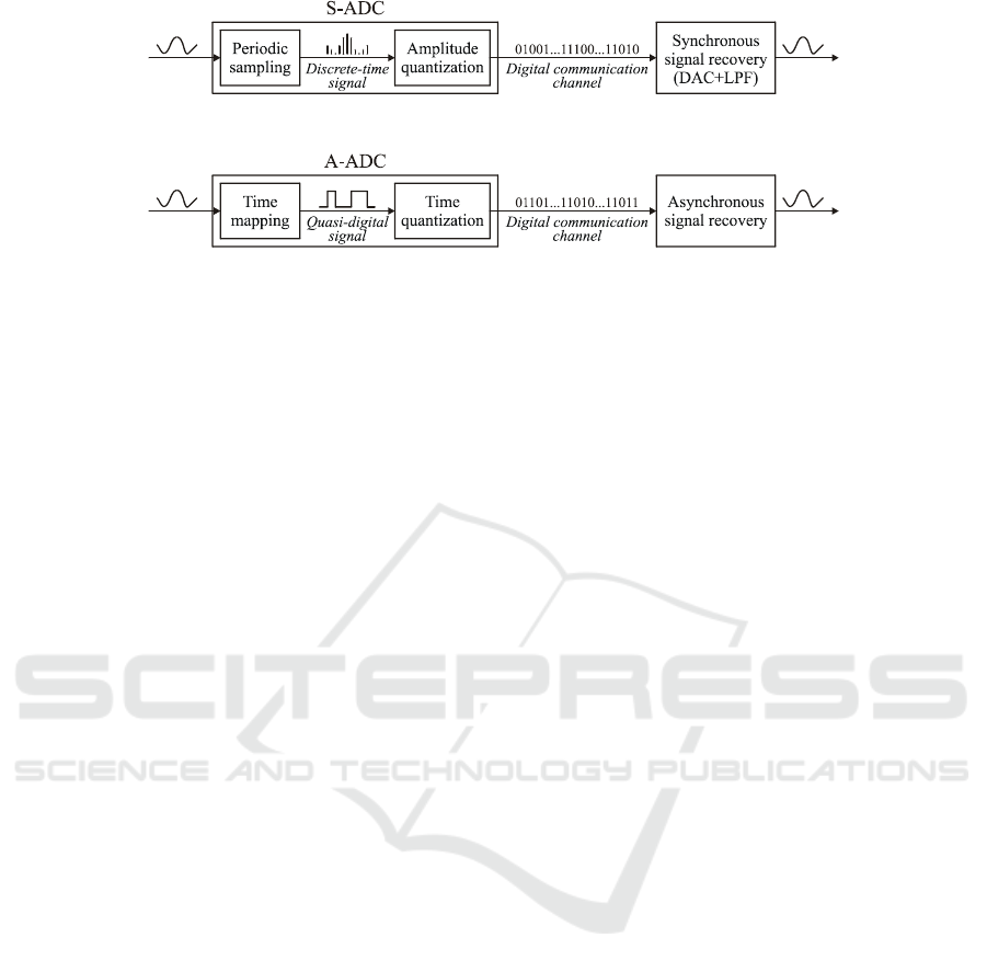
Figure 1: Traditional synchronous signal processing chain (digital numbers represent amplitude information).
Figure 2: Asynchronous signal processing chain (digital numbers represent time information).
2 ASYNCHRONOUS ADCS
To overcome problems with decreasing accuracy of
amplitude quantization, a new class of ADCs called
asynchronous analog-to-digital converters (A-
ADCs) was proposed recently where the mapping of
an analog signal into time domain rather than into
amplitude domain is used (Allier et al., 2003). In
general, the concept of time-encoding of a signal
amplitude is not new since it was used for example
in the well-known dual-slope ADCs, and in the
frequency-to-code converters. A time-based energy-
efficient ADC developed recently also uses the time
as an intermediate signal variable (Yang and
Sarpeshkar, 2005). In the asynchronous ADCs, the
time is used as the ADC output signal so binary
words that appear on the converter output irregularly
represent a sequence of time intervals instead of a
series of signal amplitude samples.
2.1 Sync Versus Async ADCs
The principle of asynchronous analog-to-digital
converters (A-ADCs) is completely different from
classical ADCs that are synchronous devices
controlled by a global clock. In the synchronous
ADCs (S-ADCs), the periodic sampling and the
amplitude quantization are applied. Instead, in the
A-ADCs, the analog signal is mapped into timing
(quasi-digital) parameters that are further quantized
according to the resolution of a reference clock.
Thus, the A-ADC operation consists in a redefinition
of domains at which the signal is sampled and
quantizated. The A-ADC does not include sample-
and-hold circuits, and is not controlled by any global
clock but self-timed. The local reference clock is
used only to quantize time intervals that represent
the converted signal amplitude. The clockless
architecture is attractive for energy-efficient design
since a global clock is the primary component of
power consumption in contemporary electronic
instrumentation. The invention of A-ADCs
announces thorough revision of the whole signal
processing chain and a development of a new
processing area called asynchronous signal
processing. The synchronous and the asynchronous
signal processing chains are presented in Figs. 1-2.
2.2 State of Art of A-ADCs Design
Although various techniques have been
accommodated to the design of low power ADCs,
the asynchronous clockless architectures based on
event-based sampling have been studied in the
context of ADCs in a few works only. Initially, the
well-known advantages of the asynchronous design
(i.e. low energy consumption, immunity to
metastable behavior, reduction of the circuit average
activity and electromagnetic interferences) have
inspired researchers to improve operation of
conventional synchronous ADCs by adoption of
solutions intrinsic for the asynchronous technology.
Such converters are locally asynchronous, but
globally synchronous since the sampling scheme is
still time-triggered and periodic (Sayiner et al.,
1996; Roza, 1997, Kinniment et al., 2000).
A postulate of a fully asynchronous ADC based
on the level-crossing sampling and the asynchronous
design has been introduced by Allier et. al (2003).
The purpose of a (fully) asynchronous ADC design
is a thorough revision of the whole signal processing
chain. In (Allier et al., 2005), the CMOS
implementation of LC-ADC with experimental
results is reported. The performance index (Figure of
Merit) of the LC-ADC is twice higher than that of a
classical synchronous ADCs. A significant
performance improvement achieved in the LC-ADC
stems from reducing the activity of the asynchronous
converter by a substitution of the periodic sampling
by the level-crossing scheme. The average rate of
the level-crossing sampling operations are lower
than the frequency of the periodic sampling because
TOWARDS ASYNCHRONOUS SIGNAL PROCESSING
179
the former are triggered if the input signal crosses
prespecified levels disposed along the amplitude
domain (compare Figs. 3a-3b), see (Miśkowicz,
2006) for details.
Akopyan et al. (2006) have designed a level-
crossing flash ADC (LCF-ADC) dedicated to real-
time monitoring and control applications where the
analog signal reconstruction is not required. Instead,
only the actual reports about a state of the observed
object are generated. Since in the LCF-ADC the
time is not tracked explicitly (i.e. the converter does
not record the times at which the samples are taken),
the power consumption is reduced additionally due
to eliminating the circuitry that deals with time
tracking. The architectures of the LCF-ADC and the
LC-ADC are completely different. The latter adopts
the feedback-based approach (Allier et al., 2003;
Allier et al., 2005), and the former utilizes a parallel
flash-type topology (Akopyan et al., 2006).
x
(
t
)
ε
max
=Δ
t
T T
x
((i+1)T)
x
(iT)
T
x
(
t
)
Δ
t
t
i-2
t
i
x
(t
i
)
x
(t
i-1
)
Δ
x
(t
i-2
)
t
i- 1
Figure 3: Comparison of the periodic (a) and the level-
crossing sampling (b) schemes for the same sampling
resolution, i.e.
Δ=
max
ε
.
Summing up, several advantages of
asynchronous ADCs in relation to conventional
synchronous ADCs can be displayed as follows. The
asynchronous ADCs are a low-cost alternative to
conventional converters due to lower energy
consumption, simple architecture, and elimination of
the global clock and the sample-and-hold circuits.
2.3 Time vs. Amplitude Quantization
Although the time quantization is in general a
complementary process to the amplitude
quantization, certain differences might be
distinguished. Whereas the analog signal amplitude
is bounded and usually a non-monotone function,
the time is a magnitude with unceasingly growing
values. As a result, each quantization of the
amplitude can be referred to a certain absolute
reference level (usually zero). Instead, a
quantization of time has to be always related to the
relative reference which is the most recent event
(i.e. a beginning of the present time interval). Next,
whereas the amplitude is a fully analog magnitude,
the frequency/time is considered as ‘quasi-digital’
domain since these parameters combine both analog
and digital signal properties (Kirianaki et al., 2002).
Furthermore, the time quantization is usually
characterized by a non-redundant conversion time.
Instead, the quantization of the amplitude takes a
non-zero conversion time, sometimes is slow (e.g. in
conventional successive-approximation ADCs), or
the conversion time is variable and dependent on the
input signal level (e.g. in delta-encoded ADCs).
Finally, the frequency references (e.g. crystal
oscillators) are more stable than the voltage
reference sources (that are sensitive to the
temperature and the technological process tolerance)
so the time quantization is in general more accurate
than the quantization in the amplitude domain.
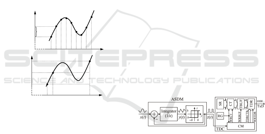
3 ASD-ADC CONCEPT
In this paper, we present a concept of analog-to-
digital conversion based on the asynchronous
Sigma-Delta modulation. The architecture of
asynchronous Sigma-Delta ADC (ASD-ADC) with
serial output interface is shown in Fig. 4.
Figure 4: The architecture of ASD-ADC with serial output
interface (TxD).
A two-level conversion scheme is utilized in the
ASD-ADC. First, the analog signal x(t) amplitude is
converted to an asynchronous square wave z(t) with
modulated frequency and duty cycle in the
asynchronous Sigma-Delta modulator (ASDM) (Fig.
5). The asynchronous square wave z(t) is a quasi-
digital signal since it is discrete in the amplitude and
continuous in the time. The widths of successive
pulses of z(t) depend on the mean value of converted
analog signal amplitude in the corresponding time
windows defined by these pulses. The width of
pulses has both a lower, and an upper bound.
To provide the digital output, the pulse widths
ICINCO 2009 - 6th International Conference on Informatics in Control, Automation and Robotics
180
are next quantized by the n-bit time-to-digital
converter (TDC). The quantization is based on
counting periods of a reference clock during each
pulse of the square wave on the ASDM output.
Finally, the digital code on the ASD-ADC output
represents time information that encodes the analog
signal amplitude. The ASD-ADC belongs to a class
of the mean value converters that are immune to
noise due to integration in the ASDM. The
asynchronous serial transmitter on the ASD-ADC
output transmits the digital words consisting of a
number of n bits of data preceded by the Start bit
and completed with the Stop bit.
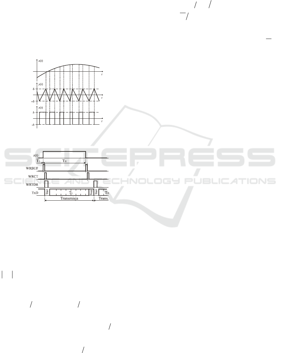
Figure 5: The waveforms on integrator output y(t), and on
ASDM output z(t) for a given signal x(t).
Figure 6: The timing of control signals in the time-to-
digital converter (TDC).
Thus, transition times of the square wave z(t) on
the output of the ASDM are non-uniformly spaced.
The output quantity, which is a sequence of lengths
of time intervals
kkk
ttt −=Δ
+1
between consecutive
transitions, depends on the input signal behavior.
The input signal x(t) has to be bounded (i.e.
ctx ≤)(
) so either the upper
max
tΔ , or the lower
bound
min
tΔ for
k
tΔ are also bounded (Lazar and
Toth, 2005) as follows:
maxmin
)]1(2[])1(2[ tTtTt
k
Δ=−
≤
Δ≤+=Δ
η
η
(1)
where
1
,
+kk
tt are time instants of the kth and the
(k+1)th transitions, respectively,
bT
κ
δ
4=
is the
self-oscillation period (i.e. the time between
consecutive slopes of z(t) if the modulator is fed by
the zero input signal), and
bc=
η
is the maximum
modulation depth. The
κ
denotes the integration
constant, and the
δ
, b are the parameters of the
Schmitt trigger (see Fig. 4). The ASDM input/output
characteristics is given by (Kościelnik, Miśkowicz,
2008):
]})1(1[2{1
k
k
k
Tt
η
−+=Δ , (2)
where
bx
kk
=
η
, )1;1(
−
∈
k
η
is the modulation
depth in the kth time window
),(
1+kk
tt
of the ASDM
defined as the ratio between the amplitude b on the
output signal z(t), and the mean signal value
k
x
of
the input signal x(t) in the time interval
),(
1+kk
tt
,
3.1 ASDM Modulator
The asynchronous Sigma-Delta modulator (ASDM)
consists of the lowpass filter (integrator), and the
Schmitt trigger operating in a negative feedback
loop (Fig. 4). For zero input signal x(t), the square
wave z(t) on the ASDM output oscillates with the
self-oscillation period (T) and ½ duty cycle. The
ASDM does not require any clocking and can
operate at low current and supply voltage since the
corresponding analog circuitry is extremely simple.
The idea of the asynchronous Sigma-Delta
modulation was formulated in the 60s (Roza, 1997).
However, a use of ASDM for signal conversion
became especially attractive because the loss-free
analog signal recovery based on ASDM output
signal was developed recently (Lazar and Toth,
2005). In (Kościelnik, Miśkowicz, 2008), the ASD-
ADC with the charge-pump integrator and with the
single output data buffering is presented. In the
present paper, we report the advanced version of the
digital interface with the double data buffering
providing the rate-based flow control.
3.2 LC-ADC vs. ASD-ADC
Our approach is motivated by several advantages of
the proposed solution comparing to level-crossing-
based ADCs (LC-ADCs) as follows.
First, in the ASD-ADC the information about the
analog signal behavior is embedded only in a
sequence of timing parameters. In other words, a
digital output includes the timing information about
the square wave on the output of the ASDM.
Instead, in LC-ADCs, the digital data on the
converter output have to include both the timing and
the one-bit amplitude information about the level-
crossing specification (Allier et al., 2003).
Second, due to integrating input properties of the
ASDM, the ASD-ADC is characterized by low
TOWARDS ASYNCHRONOUS SIGNAL PROCESSING
181

susceptibility to noise making it suitable for noisy
industrial environments. Instead, the LC-ADCs are
sensitive to non-idealities in VLSI settings of a
regular grid of amplitude levels triggering sampling
operations.
Third, unlike LC-ADCs where the maximum
time interval being encoded and digitized is
unbounded and thus has to be arbitrary controlled by
time-out, the maximum time interval in the ASD-
ADC is bounded and controlled via design process.
Finally, the sampling theorem has been
developed for ASD-based conversion by Lazar and
Toth (2005) causing to exploit the ASD-ADC in
applications where the exact recovery of original
analog signal is required (e.g. audio/speech signal
conversion). Thus, the ASD-based conversion
supports a loss-free time-encoded signal processing.
3.3 TDC Architecture
The architecture of the time-to-digital converter
(TDC) is shown in Fig. 4. The TDC consists of the
n-bit counter (CT) with setup register (SR) used for
programming initial states of the CT, the reference
generator (RG), the control module (CM) that
produces control signals for data transfer (WRCT,
WRBUF, WRTDR, TDRCTR), the intermediate
buffer (TBUF), and the transmitting buffer (TDR)
with the serial output TxD. The timing of control
signals in the TDC is shown in Fig. 6.
3.3.1 Initial State of Counter
The counting of the reference clock periods T
0
starts
from an assumed initial state of the counting module
defined by the number whose value is less than zero
because the
k
tΔ is bounded by the
min
tΔ . Thus,
only the differences
min
tt
k
Δ−Δ might be quantized
(Lazar and Toth, 2005). We have defined the
optimal number M that guarantees the best
resolution of the ASD-ADC. This number is
negative and defined as
0
4TTM −= . The optimal
initial number corresponds simply to the minimum
pulse width that equals T/4 as follows from the
formula (1) (Fig. 7).
3.3.2 Serial Output Interface
Unlike in conventional ADCs, the digital data
appear on the ASD-ADC output irregularly
according to the current variations of the analog
signal amplitude. Therefore, the serial interface has
to provide data flow control. The core of our concept
of the TDC consists in the use of a double data
buffering in the digital interface since the digital
words appear in bursts of two words on the ASD-
ADC output. This corresponds to the use of rate-
based flow control (Verissimo, Rodrigues, 2001).
The double data buffering enables overlapping a
serial transmission of the ith digital word, a storage
of the (i+1)th word, and a simultaneous quantization
of the (i+2)th pulse. Thus, the serial output interface
consists of two data buffers (TBUF and TDR) (Fig.
4). Each digital word obtained as result of counting
is recorded and stored in the intermediate buffer
(TBUF) as soon as transmission of the previous
digital word is completed (Figs. 6 and 8). If so, the
given digital word is transferred from the
intermediate buffer (TBUF) to the transmitting
buffer (TDR), which causes serial transmission of
the digital word to start.
Figure 7: Counting periods of the reference clock starting
from the negative initial state.
Figure 8: Serial asynchronous transmission on ASD-ADC
double-buffered output port (TxD) with overlapping of
transmission, storage and quantization processes (T
H
denotes the digital word representing a positive pulse, and
T
L
represents a negative one).
3.3.3 Bit Rate on Serial Output Port
With double data buffering the minimum
transmission bit rate p on the ASD-ADC serial
output port is defined as:
Tkp /2=
, where k is the
number of data bits of a digital word transmitted
including control bits (Start bit, Stop bit, and an
optional Parity bit).
3.3.4 Benefits of Double Data Buffering
By applying extra data buffering with the
intermediate buffer TBUF, two benefits are
achieved. First, the transmission bit rate on the serial
output port is reduced due to shortening time
intervals between successive digital words
transmitted. The reduction of the transmission rate
ICINCO 2009 - 6th International Conference on Informatics in Control, Automation and Robotics
182

equals (1+
η
) where 0<
η
<1 is the maximum
modulation depth of the ASDM so the best reduction
can approach 100%. For example, with typical value
η
=0.5, the reduction is equal to 50%. Slowing down
the transmission bit rate saves energy consumption.
Second, the transmission bit rate is independent of
the converted analog signal amplitude (
η
).
4 CONCLUSIONS
The ASD-ADC is an universal analog-to-digital
converter that may be used in many applications.
However, due to energy efficiency, the ASD-ADC is
dedicated to use in portable devices, especially in
sensors for environmental monitoring and for
biomedical applications that need a long battery life.
In the latter, both the wireless or skin-surface
communication between sensing devices mounted
on the body for health monitoring may be used
(Kaldy et al., 2007). In such applications, the
sensors transmit data to acquisition centers at a
remote side where the signals are processed,
analyzed and recovered if needed. Usually, the
acquisition centers access practically unlimited
power. Thus, with the invention of the ASD-ADCs,
energy-expensive components of signal processing
chain are moved from the ADC to the locations
where the energy and processing resources are
available. The solution presented in the paper may
be summarized as follows.
(1) The asynchronous Sigma-Delta analog-to-digital
converter (ASD-ADC) together with the
asynchronous analog signal recovery method (Lazar
and Toth, 2005) provides possibility to establish the
asynchronous digital signal processing chain where
the ASD-ADC output data can be transmitted via a
digital communication channel. (2) Complex and
energy-expensive components of signal processing
chain are moved from ADC to data acquisition
center where the energy and processing resources
are available. (3) The ASD-ADC digital output
represents only timing information. (4) Due to
higher stability of time/frequency references, the
time quantization is more accurate than the
voltage/current quantization. (5) Decreasing supply
voltage in general does not degrade Signal-to-Noise
Ratio (SNR) of the ASD-ADC. (6) With a double
data buffering providing the rate-based flow control
at the ASD-ADC output interface, the transmission
rate is reduced even twice compared to
(conventional) single-buffered interface; slowing
down the transmission bit rate saves energy
consumption. (7) With counting reference clock
periods from the negative initial state, the dynamic
range of the ASD-ADC is extended. (8) Finally, the
ASD-ADC has excellent DC specification.
REFERENCES
Matsuzawa, A., 2007, Design challenges of analog-to-
digital converters in nanoscale CMOS, IEICE Trans.
Electron., vol. E90-C, no 4, pp. 779-85.
Yang, H.Y., Sarpeshkar, R., 2006, A Bio-Inspired Ultra-
Energy-Efficient Analog-to-Digital Converter for
Biomedical Applications, IEEE Trans. on Circuits and
Systems-I, vol. 53, no 11, pp. 2349-2356.
Yang, H.Y., Sarpeshkar, R., 2005, A time-based energy-
efficient analog-to-digital converter, IEEE Journal of
Solid-State Circuits, vol. 40, no 8, pp. 1590–1601.
Sayiner, N., Sorensen, H.V., Viswanathan, T.R., 1996, A
level-crossing sampling scheme for A/D conversion,
IEEE Trans. on Circuits and Systems II, vol. 43, no 4,
pp. 335-9.
Roza, E., 1997, Analog-to-digital conversion via duty-
cycle modulation, IEEE Trans. on Circuits and
Systems-II, vol. 44, no 11, pp. 907–914.
Kinniment, D., Yakovlev, A., Gao B., 2000, Synchronous
and asynchronous A-D conversion, IEEE Trans. on
VLSI Systems, vol. 8, no 2, pp. 217-220.
Allier, E., Sicard, G., Fesquet L., Renaudin, M., 2003, A
new class of asynchronous A/D converters based on
time quantization”, In ASYNC’03, IEEE Intern.
Symposium on Asynchronous Circuits and Systems,
pp. 196-205.
Allier, E., Goulier, J., Sicard, G., Dezzani, A., André, E.,
Renaudin, M., 2005, A 120nm low power
asynchronous ADC, In ISLPED 2005, International
Symposium on Low Power Electronics and Design, pp.
60-65.
Miśkowicz, M., 2006, Send-on-delta concept: an event-
based data reporting strategy, Sensors, vol. 6, no 1, pp.
49-63.
Akopyan, F., Manohar, R., Apsel, A. B., 2006, A level-
crossing flash asynchronous analog-to-digital
converter, In ASYNC’06, IEEE International
Symposium on Asynchronous Circuits and Systems,
pp. 12-22.
Kościelnik, D., Miśkowicz, M., 2008, Asynchronous
Sigma-Delta analog-to digital converter based on the
charge pump integrator, Analog Integrated Circuits &
Signal Processing, vol. 55, no 3, pp. 223–238.
Lazar, A.A., Tóth, L.T., 2005, Perfect recovery and
sensitivity analysis of time encoded bandlimited
signals, IEEE Trans. on Circuits and Systems-I, vol.
51, no 10, pp. 2060-2073.
Verissimo P., Rodrigues L., 2001, Distributed Systems for
System Architects, Kluwer Academic Publishers.
Kaldy, C., Lazar, A.A., Simonyi, E.K., Toth, Laszlo T.,
2007, Time Encoded Communications for Human
Area Network Biomonitoring, Technical Report, Depart-
ment of Electrical Engineering, Columbia University.
TOWARDS ASYNCHRONOUS SIGNAL PROCESSING
183
