SYNTHESIS OF THE LOW-PASS AND HIGH-PASS WAVE DIGITAL
FILTERS
B. Psenicka, F. Garcia-Ugalde and A. Romero Mier y Teran
Universidad Nacional Autonoma de M
´
exico, Mexico
Keywords:
Wave Digital Filter, Algorithm, Implementation in DSP.
Abstract:
In this paper we propose a very simple procedure for the design and analysis of low-pass and high-pass wave
digital filters derived from reference filter given in the lattice configuration. Wave Digital Filters derived from
reference filter in lattice configuration can be designed with excellent pass band properties. They can be
proposed and implemented without the knowledge of classical filter theory. In this paper we present tables
for Butterworth, Chebychev and Elliptic low-pass filter design. In the examples we demonstrate programs in
MATLAB that permits analyze the attenuation properties of the designed filters. In the end of our article we
realize wave digital filter using Embedded Target for Texas instruments TMS320C6000 DSP Platform. The
model of the WDF was created by means of serial and parallel blocks that were added to the window Simulink
Library Browser between common Used Blocks.
1 INTRODUCTION
Wave digital lattice filters are derived from LC-filters.
The reference filter consists of parallel and serial con-
nections of several elements. Since the load resistance
R
L
is not arbitrary but dependent on the element or
source to which the port belongs, we cannot simply
interconnect the elements to a network. The elements
of the filters are connected with the assistance of serial
and parallel adapters. These adapters in the discrete
form are connected in one port by delay elements.
The possibility of changing the port resistance can
be achieved using parallel and serial adapters. These
adapters contain the necessary adders, multipliers and
inverters. In this paper we use adapters with three
ports. The block of the serial and parallel adapter and
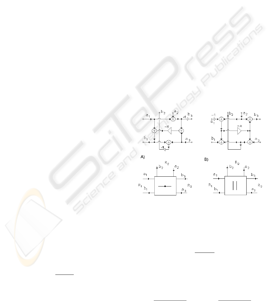
theirs signal-flow diagram are shown in figures 1 and
2. (Fettweis, 1973)
The coefficient of the 3-port reflection-free serial
adapter in figure 1A) is calculated from the port re-
sistances R
i
i=1,2 by equation (1). (Fettweis and
Meerkoetter, 1975)
B =
R
1
R
1
+ R
2
(1)
The coefficient of the reflection-free parallel adapter
in figure 1B) can be calculated from the port conduc-
tances G
i
i=1,2 by eq. (2).
Figure 1: A) Three port serial adapter whose port 3 is
reflection-free and its signal flow-graph, B) Three port par-
allel adapter whose port 3 is reflection-free and its signal
flow-graph.
A =
G
1
G
1
+ G
2
(2)
The coefficients of the dependent parallel adapter in
the figure 2B) can be get from the port conductances
G
i
i=1,2,3 by eq. (3)
A
1
=
2G
1
G
1
+ G
2
+ G
3
A
2
=
2G
2
G
1
+ G
2
+ G
3
(3)
225
Psenicka B., Garcia-Ugalde F. and Romero Mier y Teran A. (2008).
SYNTHESIS OF THE LOW-PASS AND HIGH-PASS WAVE DIGITAL FILTERS.
In Proceedings of the Fifth International Conference on Informatics in Control, Automation and Robotics - SPSMC, pages 225-231
DOI: 10.5220/0001479302250231
Copyright
c
SciTePress
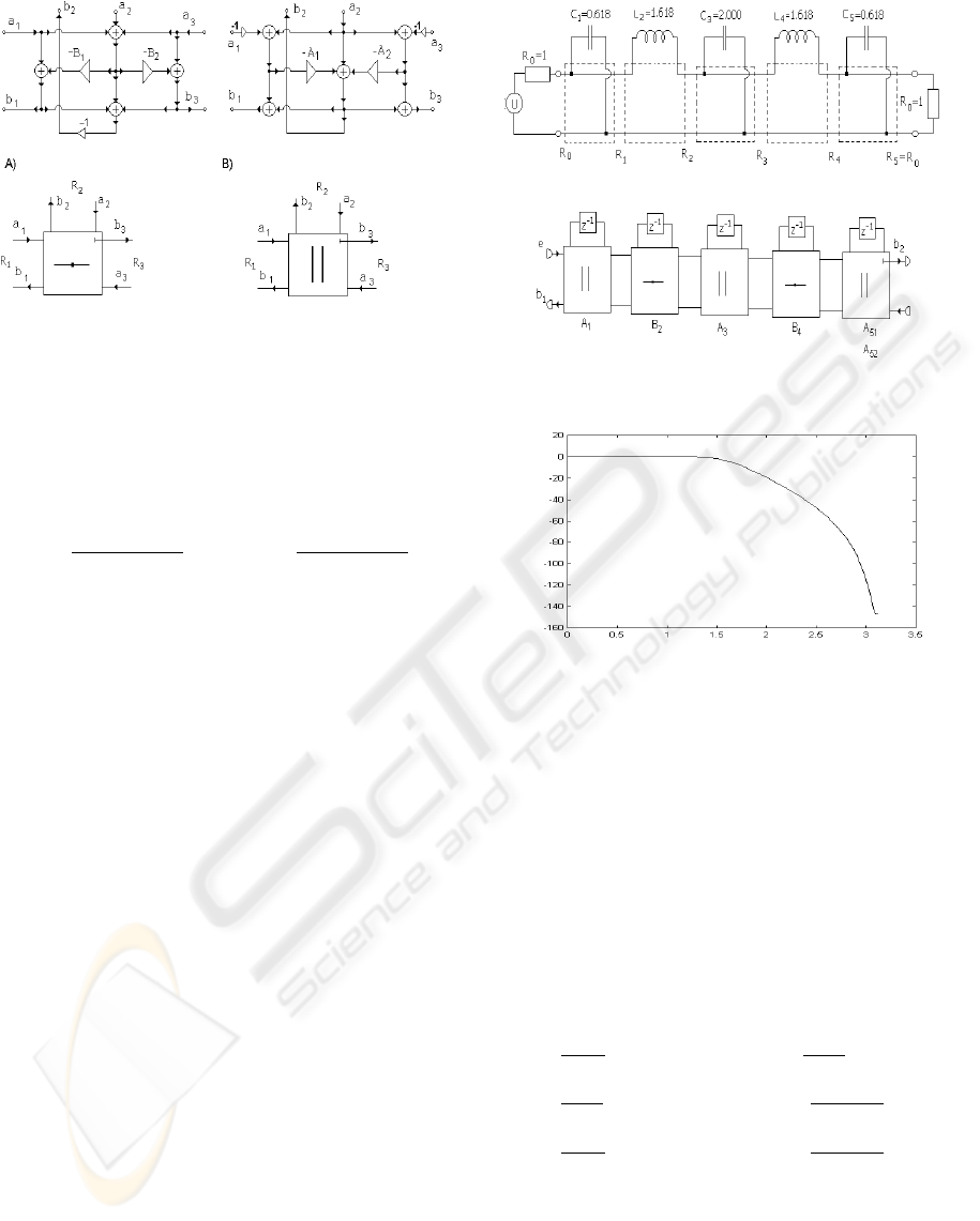
Figure 2: A) Three port serial dependent adapter and its
signal flow-graph, B) Three port parallel dependent adapter
and its signal flow-graph.
The coefficient of the dependent serial adapter in the
figure 2A) can be obtained from the port resistances
R
i
i=1,2,3 by (4)
B
1
=
2R
1
R
1
+ R
2
+ R
3
B
2
=
2R
2
R
1
+ R
2
+ R
3
(4)
When connecting adapters, the network must not con-
tain any feedback loops without a delay element in or-
der to guarantee that the structure is realizable. This
means that we cannot connect the dependent adapters
from figure 2A) and 2B). The three-port dependent
parallel adapter is reflection free at port 3 if G
3
=
G
1
+ G
2
and three port dependent serial adapter is re-
flection free if R
3
= R
1
+ R
2
.
2 EXAMPLES
In this part we shall demonstrate in the examples cal-
culation of the low-pass and high-pass wave digital
filter. The most important components for the real-
ization of wave digital filters according to the Fet-
tweis procedure are the ladder LC filters. The tables
for wave digital structures was designed for the cor-
ner frequency f
1
= 1/(2· π) = 0.159155 and sampling
frequency f
s
= 0.5
2.1 Realization of the Low-pass Filter
In the first example we shall realize Butterworth low-
pass of the 5
th
order and A
max
= 3dB. In the figure
3 we show the structure of a 5
th
order ladder LC ref-
erence Butterworth filter and its corresponding block
connection in the digital form.
First we must calculate from FIG. 3 wave port resis-
tances R
1
,R
2
,R
3
,R
4
, and finally the coefficients of the
Figure 3: LC reference Butterworth low-pass filter and its
corresponding block connection.
Figure 4: Frequency response of the Butterworth low-pass
filter.
parallel and serial adapters A
1
,B
2
,A
3
,B
4
and the coef-
ficients of the dependent parallel adapter A
51
,A
52
ac-
cording to equations (1)-(3).
G
1
= G
0
+C
1
= 1.618 G
3
= G
2
+C
3
= 2.447
R
1
= 1/G
1
= 0.618 R
3
= 1/G
3
= 0.408
R
2
= R
1
+ L
2
= 2.236 R
4
= R
3
+ L
4
= 2.026
G
2
= 1/R
2
= 0.447 G
4
= 1/R
4
= 0.493
A
1
=
G
0
G
1
+C
1
= 0.618 B
4
=
R
3
R
3
+L
4
= 0.201
B
2
=
R
1
R
1
+L
2
= 0.276 A
51
=
2G
4
G
4
+C
5
+G
5
= 0.443
A
3
=
G
2
G
2
+C
3
= 0.182 A
52
=
2C
5
G
4
+C
5
+G
5
= 0.556
The program for the analysis of the wave digital fil-
ter of the 5
th.
order written in MATLAB follows, and
the frequency response obtained by MATLAB is pre-
sented in the figure 4. The equation in the program for
computing XN1-XN4, BN4-BN1, N1-N9 and YN(i)
was received from the structure in the Fig. 5
ICINCO 2008 - International Conference on Informatics in Control, Automation and Robotics
226
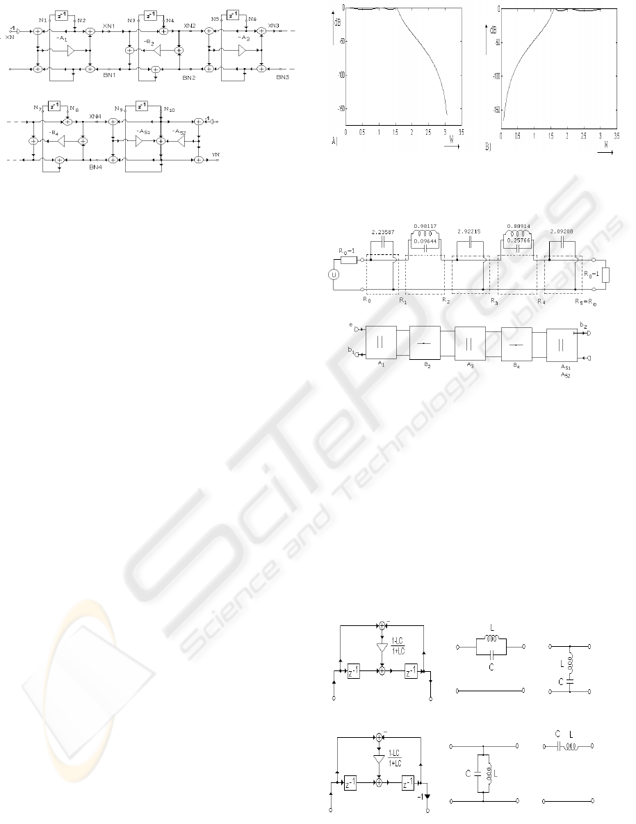
Figure 5: Butterworth wave digital low-pass filter of the 5
th
order.
A1=0.618146; B2=0.276524; A3=0.182858;
B4=0.201756; A51=0.467553; A52=0.947276;
N2=0; N4=0; N6=0; N8=0; N10=0; XN=1;
for i=1:1:50
XN1=A1*XN-A1*N2+N2; XN2=XN1+N4;
XN3=-A3*XN2-A3*N6+N6; XN4=XN3+N8;
BN4=XN4-A51*XN4+2*N10-A51*N10-A52*N10;
BN3=XN3-B4*XN4-B4*BN4;
BN2=XN2-A3*XN2+BN3+N6-A3*N6;
BN1=XN1-B2*XN2-B2*BN2;
N1=XN*A1-A1*N2+BN1; N3=BN1+BN2;
N5=-A3*XN2-A3*N6+BN3; N7=BN3+BN4;
N9=-A51*XN4+N10-A51*N10-A52*N10;
YN(i)=-A51*XN4+2*N10-A51*N10-A52*N10
N2=N1; N4=N3; N6=N5; N8=N7; N10=N9; XN=0;
end
[h,w]=freqz(YN,1,50)
plot(w,20*log10(abs(h)))
2.2 Design of the Low-pass and
High-pass Chebychev Filter
In the second example we shall propose low-pass
and high-pass Chebychev WDF for n=5, A
max
= 3
dB. From the table 4 we get the values of the WDF
A
1
= 0.223, B
2
= 0.226, A
3
= 0.182, B
4
= 0.192,
A
5,1
= 0.383 and A
5,2
= 0.360. Using previous MAT-
LAB program we obtain the attenuation of the Cheby-
chev filter presented in the Fig. 6. High-pass we get
by changing in the preceding program N2=-N1, N4=-
N3 N6=-N5, N8=-N7 and N10=-N9.
2.3 Realization of the Low-pass Cauer
WDF
In the figure 7 the structure of the 5
th
order ladder LC
reference Cauer low-pass filter is shown. The values
of the LC filter was obtained from the table C 0550
for Θ = 30
o
for A
max
= 1.2494 dB, A
min
= 70.5 dB
and Ω
s
= 2.0000 (Saal, 1979). Parallel resonant LC
circuits in the low-pass filter Fig. 7 will be realized
Figure 6: Frequency response of the low-pass and high-pass
Chebychev filter.
Figure 7: LC reference Cauer low-pass filter.
by digital structure according the Fig. 8.
With the assistance of the following MATLAB pro-
gram we can calculate coefficients of the WDF A
1
,
B
2
, A
3
, B
4
, A
51
and A
52
. The attenuation of the low-
pass Cauer filter is presented in Fig. 9. The program
was obtained from the structure in the Fig. 10. The
input data of the LC filter was obtained from the cat-
alog of the Cauer filter (Saal, 1979).
C(1)=2.235878; C(3)=2.922148; C(5)=2.092084;
L(2)=0.981174; L(4)=0.889139; C(2)=0.096443;
Figure 8: Discrete realization of parallel and serial LC cir-
cuits.
SYNTHESIS OF THE LOW-PASS AND HIGH-PASS WAVE DIGITAL FILTERS
227
Figure 9: Frequency response of the Cauer low-pass and
high-pass filter.
Figure 10: Structure of the Cauer low-pass filter n=5.
C(4)=0.257662; XN=1; N2=0; N4=0; N6=0; N6=0;
N8=0; N10=0; N12=0; N14=0; G(1)=1;
G(2)=G(1)+C(1); R(2)=1/G(2);
R(3)=R(2)+1/(C(2)+1/L(2));
G(3)=1/R(3); G(4)=G(3)+C(3); R(4)=1/G(4);
R(5)=R(4)+1/(C(4)+1/L(4)); G(5)=1/R(5);
K(2)=(L(2)*C(2)-1)/(L(2)*C(2)+1);
K(4)=(L(4)*C(4)-1)/(L(4)*C(4)+1);
A(1)=G(1)/G(2); B(2)=R(2)/R(3);
A(3)=G(3)/(G(3)+C(3));
B(4)=R(4)/R(5); A(5,1)=2*G(5)/(G(5)+C(5)+1);
A(5,2)=2/(G(5)+C(5)+1);
for i=1:1:500
XN1=A(1)*XN+N2-A(1)*N2; XN2=XN1+N6;
XN3=-A(3)*XN2+N8-A(3)*N8; XN4=XN3+N12;
BN4=XN4-XN4*A(5,1)+2*N14-N14*A(5,1)-A(5,2)*N14;
BN3=-BN4*B(4)+XN3-B(4)*XN4;
BN2=XN2-A(3)*XN2+BN3+N8-A(3)*N8;
BN1=XN1-XN2*B(2)-BN2*B(2);
N1=XN*A(1)-N2*A(1)+BN1; N3=BN1+BN2;
N5=-K(2)*N3+K(2)*N6+N4; N7=-XN2*A(3)+BN3-N8*A(3);
N9=BN3+BN4; N11=N10-N9*K(4)+N12*K(4);
N13=-A(5,1)*XN4+N14-A(5,1)*N14-A(5,2)*N14;
YN(i)=-A(5,1)*XN4+2*N14-A(5,2)*N14-A(5,1)*N14;
N2=N1; N4=N3; N6=N5; N8=N7; N10=N9; N12=N11;
N14=N13; XN=0;
end
[h,w]=freqz(YN,1,500); plot(w,20*log10(abs(h)))
High-pass can be obtained by changing in pro-
gram N2=-N1, N4=-N3 N6=-N5, N8=-N7, N10=-N9,
N12=-N11, N14=-N13. In the Fig. 9 the attenuation
of low-pass and high-pass filter are presented.
2.4 Realization of Wave Digital Filters
in DSP C6711 by Simulink
The simulink model showed in Figure 11 corresponds
to the realization of a wave digital filter applica-
tion on TMS320C6711 DSK using Embedded Tar-
get for Texas Instruments TMS320C6000 DSP Plat-
form. The model of the WDF was created by means
of serial and parallel block that were added to the
window Simulink Library Browser between Com-
monly Used Blocks. In the input and output of the
WDF were added ADC and DAC convertes of the
TMS320C6711 that are in the window Simulink Li-
brary Browser, Embedded Target for TI C6000 DSP
and C6711DSK Board Support. This model created
in Code Composer Studio project can be see in Fig-
ure 13 and can run on the DSP C6711.
Figure 11: Realization of Wave Digital Filter in
TMS320C6711 by Simulink.
Figure 12: Realization of Wave Digital Filter in
TMS320C6711 by Simulink.
ICINCO 2008 - International Conference on Informatics in Control, Automation and Robotics
228
Figure 13: Realization of Wave Digital Filter in
TMS320C6711 by Simulink.
3 CONCLUSIONS
Though the structure of the wave digital filter is more
complicated than other structures, the algorithm for
implementation on the DSP is very simple and it is
very easy to propose the general algorithm for the ar-
bitrary order of the filter. These structures are not so
sensitive to the error of quantization as other types of
the filters. With small modification of the presented
programs can be created another tables of the WDF.
The parts of the programs can be utilized for imple-
menting of the wave digital filters in digital signal pro-
cessors DSP.
REFERENCES
Fettweis, A. (1973). Digital filter structures related to clas-
sical filter networks. In Arch. Electron. Uebertragung-
stechnik. AEU.
Fettweis, A. and Meerkoetter, K. (1975). On adaptors for
wave digital filters. In IEEE Trans. on Accoustics,
Speech and Signal Processing. IEEE.
Saal, R. (1979). Handbuch zum filterentwurf. In AEG Tele-
funken. AEG Telefunken.
APPENDIX
Tables of the Wave Digital Filters
Tables of the Butterworth Wave Digital Filters
In the Fig. 14 is the tolerance scheme of the Butter-
worth filter and in the Fig. 15 is the structure of the
Butterworth Wave Digital Filter (WDF).
The structure is created by cascade connection of the
parallel and serial adapters. If at the begin is paral-
lel reflection free adapter, at the end of the structure
in case n odd must be connected parallel dependent
adapter in order to realize load resistance R
L
. In case
n even at the end we have to connect serial dependent
adapter.
In the table 2 are the elements of the Butterworth
WDF for various attenuation A
max
in the passband.
A
i
and B
i
are the coefficients of the parallel and serial
adapters respectively.
Figure 14: Attenuation of Butterworth WDF.
Figure 15: Digital structure of Butterworth WDF.
Tables of the Chebychev Wave Digital Filter
In Fig. 16 is the tolerance scheme and the attenua-
tion of the the Chebychev filter. The structure of the
Chebychev wave digital filters is demonstrated in the
Fig. 17. This structure is created by connection of
SYNTHESIS OF THE LOW-PASS AND HIGH-PASS WAVE DIGITAL FILTERS
229
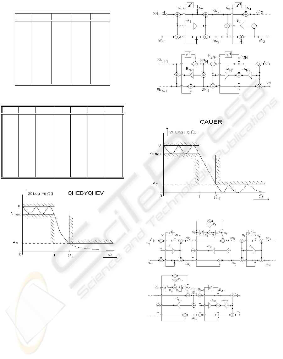
Table 1: Elements of Butterworth WDF n=3, A
max
in [dB].
A
max
A
1
B
2
A
31
A
32
0.1 0.6519 0.3790 0.5497 0.9454
0.2 0.6248 0.3422 0.5099 0.9310
0.3 0.6083 0.3209 0.4858 0.9211
0.4 0.5964 0.3059 0.4685 0.9134
0.5 0.5864 0.2943 0.4548 0.9069
0.6 0.5791 0.2849 0.4434 0.9014
0.7 0.5723 0.2769 0.4337 0.8964
0.8 0.5664 0.2700 0.4252 0.8920
0.9 0.5611 0.2639 0.4176 0.8878
1.0 0.5562 0.2585 0.4208 0.8840
Table 2: Elements of Butterworth WDF n=5, A
max
in [dB].
A
max
A
1
B
2
A
3
B
4
A
51
A
52
0.1 0.702 0.387 0.286 0.318 0.602 0.981
0.2 0.687 0.365 0.265 0.295 0.578 0.972
0.3 0.678 0.353 0.253 0.281 0.563 0.974
0.4 0.671 0.344 0.244 0.271 0.553 0.971
0.5 0.666 0.337 0.238 0.264 0.544 0.969
0.6 0.662 0.331 0.232 0.258 0.537 0.968
0.7 0.658 0.326 0.228 0.252 0.531 0.966
0.8 0.655 0.322 0.224 0.248 0.526 0.965
0.9 0.652 0.318 0.220 0.244 0.521 0.964
1.0 0.649 0.314 0.217 0.240 0.517 0.962
Figure 16: Attenuation of Chebychev WDF.
the parallel and serial adapters terminated at the port
3 with delay element. At the end of the structure must
be connected parallel dependent adapter to realize for
n odd load resistance R
L
= 1.
In table 4 are the elements of the Chebychev WDF
for various attenuation A
max
in the passband and or-
der filter n=5. The tables was designed for sampling
frequency f
s
= 0.5.
Tables of the Cauer Wave Digital Filters
In the Fig 18 is the attenuation of the Cauer WDF.
The structure of the Cauer WDF is presented in the
Fig 19. LC parallel resonant circuits in longitudinal
branch are realized by serial adapters connected in the
3
rd
port with two delay elements. The filter with n odd
Figure 17: Structure of Chebychev WDF filter.
Figure 18: Attenuation of Cauer WDF.
Figure 19: Digital structure of Cauer WDF.
must be terminated with parallel dependent adapter.
In the tables 5 and 6 are the elements of the Cauer
WDF for various attenuation A
max
in passband and
sampling frequency f
s
= 0.5. In the next section we
shall demonstrate in the examples calculation of the
Wave digital low-pass and high-pas filters.
ICINCO 2008 - International Conference on Informatics in Control, Automation and Robotics
230
Table 3: Elements of Chebychev WDF n=3, A
max
in [dB].
A
max
A
1
B
2
A
31
A
32
0.10 0.4922 0.3022 0.4620 0.7574
0.25 0.4341 0.2774 0.4310 0.6812
0.50 0.3852 0.2599 0.4126 0.6114
1.00 0.3307 0.2496 0.3995 0.5293
2.00 0.2695 0.2445 0.3929 0.4331
3.00 0.2300 0.2442 0.3925 0.3696
Table 4: Elements of Chebychev WDF n=5, A
max
in [dB].
A
max
A
1
B
2
A
3
B
4
A
51
A
52
0.10 0.465 0.253 0.216 0.224 0.417 0.737
0.25 0.419 0.240 0.205 0.213 0.398 0.672
0.50 0.369 0.231 0.197 0.204 0.386 0.596
1.00 0.319 0.226 0.191 0.198 0.379 0.516
2.00 0.261 0.225 0.185 0.193 0.379 0.422
3.00 0.223 0.226 0.182 0.192 0.383 0.360
Table 5: Elements of Cauer WDF n=3, Ω
s
= 4.8097, K
2
=
−0.93686.
A
m
A
s
A
1
B
2
A
31
A
32
0.0004 24.7 0.7504 0.5766 0.7314 0.9629
0.0017 30.7 0.7209 0.4907 0.6664 0.9374
0.0039 34.3 0.6673 0.4569 0.6272 0.9160
0.0109 38.7 0.6190 0.4063 0.5778 0.8803
0.0279 42.8 0.5706 0.3612 0.5339 0.8365
0.0436 44.8 0.5461 0.3459 0.5140 0.8114
0.0988 48.3 0.4983 0.3161 0.4804 0.7573
0.1773 50.9 0.4614 0.2979 0.4590 0.7110
0.2803 53 0.4306 0.2855 0.4442 0.6699
1.2494 60 0.3147 0.2593 0.4118 0.4999
Table 6: Elements of Cauer WDF n=5, Ω
s
= 2.0000 K
2
=
−0.827 K
4
= −0.627.
A
max
A
s
A
1
B
2
A
3
B
4
A
51
A
52
0.0017 41.3 0.657 0.399 0.330 0.436 0.734 0.915
0.0039 44.8 0.627 0.373 0.311 0.404 0.690 0.893
0.0109 49.2 0.585 0.343 0.290 0.369 0.639 0.856
0.0279 53.3 0.543 0.318 0.272 0.341 0.596 0.813
0.0510 55.3 0.522 0.306 0.264 0.323 0.577 0.788
0.0988 58.8 0.479 0.288 0,251 0.310 0.546 0.736
0.1773 61.4 0.446 0.277 0.243 0.298 0.527 0.691
0.2803 63.5 0.418 0.270 0.237 0.289 0.514 0.652
1.2494 70.5 0.309 0.256 0.221 0.269 0.492 0.487
SYNTHESIS OF THE LOW-PASS AND HIGH-PASS WAVE DIGITAL FILTERS
231
