
BIOSIGNAL ACQUISITION DEVICE
A Novel Topology for Wearable Signal Acquisition Devices
Luca Maggi, Luca Piccini, Sergio Parini, Giuseppe Andreoni
Dipartimento di Bioingegneria of Politecnico di Milano - Milan, Italy
Guido Panfili
SXT – Sistemi per telemedicina srl. – Lecco, Italy
Keywords: Wearable device, Brain Computer Interface, Amplifier, Signal Conditioning, Offset Recovery, Low Voltage
Amplifier, Band Pass Filtering, ECG amplifier, EEG amplifier.
Abstract: The here presented work illustrates a novel circuit topology for the conditioning of biomedical signals. The
system is composed of an amplification chain and relies on a double feedback path which assures the
stability of the system, regardless of the amplification block gain and the order of the low-pass filter
settings. During the normal operation, the offset recovery circuit has a linear transfer function, when it
detects a saturation of the amplifier, it automatically switches to the fast recovery mode and restores the
baseline in few milliseconds. The proposed configuration has been developed in order to make wearable
biosignal acquisition devices more robust, simpler and smaller. Thanks to the used AC coupling method,
very low high-pass cut-off frequencies, can be achieved even using small valued passive components with
advantages in terms of circuit bulkiness. The noise rejection filter between the pre-amplification and the
amplification stages eliminates the out-of-band noise before the amplification reducing the possibility of
having clipping noise and minimizing the dynamic power consumption. The presented topology is currently
used in a prototypal EEG acquisition device in a Brain Computer Interface (BCI) system, and in a
commercial polygraph which will be soon certificated for clinical use.
1 INTRODUCTION
Wearable systems ought to be totally unobtrusive
devices that allow physicians to overcome the
limitations of standard ambulatory technology,
aiming at providing a response to the need for
monitoring individuals over weeks or even months
without or limiting their usual behaviour. Such a
systems typically rely on wireless, miniature sensors
embedded in patches, bandages, or in items that can
be worn, such as a ring or a shirt. They take
advantage of hand-held units to temporarily store
physiological data, which can be uploaded
periodically to a database server through a wireless
LAN or different gateways that allow Internet
connection. The data sets recorded using these
systems are then processed to detect events able to
indicate a possible worsening of the patient’s clinical
situation or providing information explored to assess
the impact of clinical interventions (Park, 2003).
Wearable devices are usually battery powered:
low voltage supply and low power consumption are
mandatory features for this kind of devices, in order
to provide a good battery life to dimension ratio. In
the last 10 years many garments with embedded
sensors have been developed: the intrinsic
characteristics of such electrodes and the possible
instability of the contact make the design of
wearable acquisition devices more difficult
(Webster, 1991). The main aspects we have to take
into account in the design of a wearable surface
biopotential amplifier (e.g. Electrocardiogram-ECG,
Electroencephalogram–EEG and Electromiogram-
EMG) are:
• Dynamic reserve;
• Max offset rejection;
• Fast recovery from artefacts.
Although the operational amplifiers production
technology has developed several low power and
low cost devices, the development of dedicated
397
Maggi L., Piccini L., Parini S., Andreoni G. and Panfili G. (2008).
BIOSIGNAL ACQUISITION DEVICE - A Novel Topology for Wearable Signal Acquisition Devices.
In Proceedings of the First International Conference on Bio-inspired Systems and Signal Processing, pages 397-402
DOI: 10.5220/0001059703970402
Copyright
c
SciTePress
topologies is still necessary in order to maximize the
overall circuit performance.
2 METHODS
2.1 Background
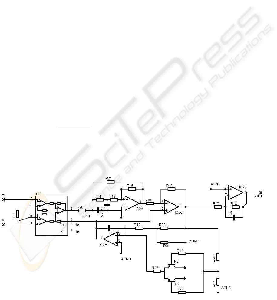
Figure 1 shows a typical, state of the art biosignal
detection circuit which is composed of a set of
independent stages connected in a chain. At the
beginning there is a pre-filtering stage, the pre-
amplification stage which is followed by the offset
rejection circuit and by an amplification and filtering
circuit.
This kind of solution is simple and effective when
the wide power supply range provides a high
dynamic reserve (avoiding clipping problems) and
when the mechanical specifications allow the use of
high capacity capacitor or the specific application
doesn’t require very low frequency high pass filter.
It is worth to underline that the maximum tolerable
offset is given by the following equation:
preamp
MAX
Off
G
VV
V
)(
*
2
1
supsup
−+
−
≅
(1)
Where V
sup
are the value of the supply rails and
G
preamp
is the gain of the preamplification stage.
It is worth noting that in case of a change in the
input signal that causes the amplifier saturation, the
output of the system will remain latched for a time
which depends on the signal amplitude; it is possible
to overcome this limitation by increasing the system
complexity and inserting a baseline reset circuit
which is activated by the saturation of the system
itself.
2.2 General Description
The proposed system is composed of a differential
pre-amplification stage P(s): usually realized using
an Instrumentation Amplifier (INA). The F(s) block
is a unity gain inverting filter (low-pass or low-pass
plus notch filter) of any order. A(s) is an
amplification stage, while I(s) is an offset
compensation network. In the proposed version it is
a non-linear circuit which acts as an attenuated
inverting integrator when the Vin is inside the linear
region and as an amplified inverting integrator when
the signal is over threshold whose behaviour can be
expressed as follow:
sup sup
11
1
in
if V Th V V Th
asRC
I
kotherwise
sRC
−+
⎧
−
+<< −
⎪
⎪
=
⎨
⎪
−
⎪
⎩
(2)
where Th is threshold value which identifies a
saturated state, ‘a’ is an attenuation factor and ‘k’
the amplification factor.
The small signal transfer function and the G
Loop
of the system are represented by the following
equation:
)](1)[()(
]1)()[()(1
)()(
)()(
sFsIsAG
sFsAsI
sAsF
sPsTF
LOOP
−=
−−
⋅=
(3)
Figure 1: The amplification chain proposed by the OpenEEG project.
BIOSIGNALS 2008 - International Conference on Bio-inspired Systems and Signal Processing
398
Figure 2: Block structure of the system.
considering that I(s) and F(s) are inverting the
equation can be expressed as follows:
]1)([)()(
]1)([)()(1
)()(
)()(
+⋅⋅−=
+⋅⋅−
⋅=
sFsIsAG
sFsAsI
sAsF
sPsTF
LOOP
(4)
The transfer function is a band-pass amplifier with a
single pole high-pass and a low-pass whose shape
depends on F(s). Figure 3 shows the bode diagram
of a system with the following characteristics:
• F(s): 2
nd
order low pass at 75Hz;
• A(s): amplifier gain 100 V/V;
• P(s): pre-amplifier gain 5V/V;
• I(s): integrator 1/100 * 1/s.
Figure 3: Frequency response of a sistem with 500V/V
gain and a 2nd order low pass 75Hz filter.
2.3 Offset Compensation Issues
On the basis of the final output, the offset
compensation value is fed both directly to the
preamplifier P(s) reference pin, and by modifying
polarization of the amplifier A(s). The proposed
structure introduces a systemic offset compensation
method which ensures that, thanks to the double
feedback path, even when the pre-amplification
output is close to the power supply rail, the
following stages work inside the linear region this
property doubles the maximum tolerable offset:
pream
MAX
Off
G
VV
V
)(
supsup
−+
−
≅
(5)
Thanks to this improvement it is possible to increase
the gain of the pre-amplification stage taking major
advantages of the qualities of the INA in terms of
CMRR a noise figure.
As proposed in our previous work, the AC-
coupling of the amplifier using a feedback integrator
allows the tuning of the high-pass pole frequency
just by varying the open loop gain of the system
(Maggi, 2004). When setting the parameters for
biosignals acquisition, it is useful to insert an
attenuation factor in the I(s) block in order to
compensate the amplifier gain: keeping the G
loop
below the unity gain the high pass pole is moved to
the lower frequencies.
The I(s) automatically identifies a saturation of
the amplifier using a threshold method: if the value
is outside a predefined interval, the attenuated
integrator is switched into an amplified integrator
that quickly brings the system output inside the
linear interval.
The k value defines the delay of the offset
recovery of the system: for example we can have a
0.05Hz high pass pole during the linear phase and
switch it to a 100Hz one during the offset recovery
phase, achieving a baseline recovery in about 10ms.
2.4 Stability of the Loop
During the normal operation the G
loop
is usually kept
low using the attenuation net of I(s) in order to
achieve the desired high-pass frequency; when the
BIOSIGNAL ACQUISITION DEVICE - A Novel Topology for Wearable Signal Acquisition Devices
399
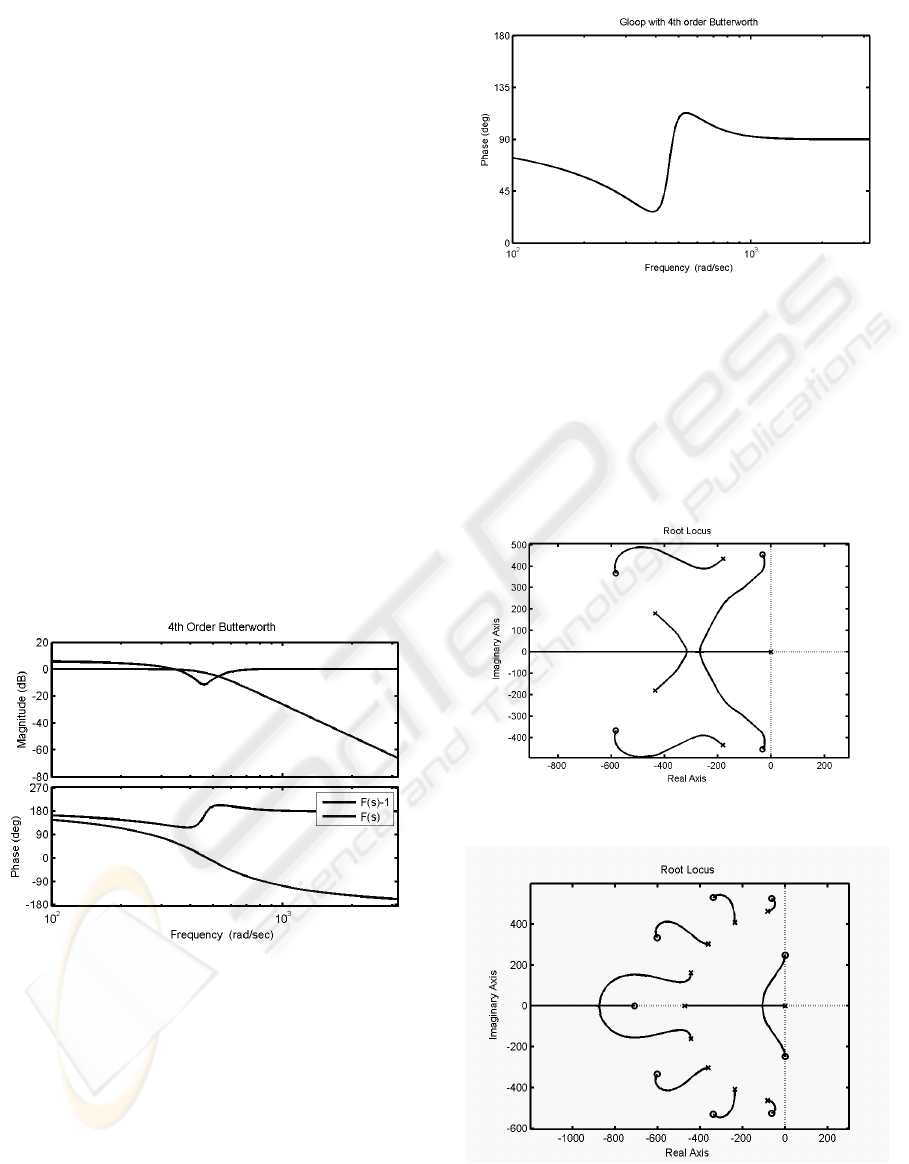
saturation occurs the I(s) is switched to a high gain
configuration: in this section the stability of this
configuration will be discussed both by considering
the Bode Stability Criterion and the root-locus
method.
2.4.1 Bode Stability Criterion
Provided that A(s) have a sufficient bandwidth to be
considered like an ideal amplifier and that F(s) and
I(s) are stable, the poles in F(s) and I(s) are the
possible instability causes of the system.
Considering the open-loop transfer function, the I(s)
provides a single pole at low frequencies, while the
F(s) put a variable number of poles at the higher
bandwidth limit. Thanks to the second feedback path
the poles of F(s) are compensated by the same
number of zeroes. The figure 4 shows the Bode
diagram of the original F(s) and the compensated
one.
The newly created zeros must be very close to the
F(s) poles in order to allow a difference between the
DC gain and the high frequency one of just 6dB. The
nearness of poles and zeroes makes the phase plot
very flat: for any complexity of the filter the plot is
between +90 and +270 degrees.
Figure 4: Bode plot of the compensate filter against the
original one.
Figure 5 shows the phase diagram of the resulting
G
loop
, including the pole introduced by the
integration process, it is possible to notice that it
never cross the instability region.
Figure 5: Phase diagram of the resulting Gloop.
2.4.2 Root Locus Study
The root locus (figure 6 and 7) show that the all the
resulting closed loop poles are in the left semi-plane
even with a 9th order low pass filter. For the higher
open loop gains the phase margin can be less than 45
degrees, but during the nonlinear phase the
overshoot can make the settling faster.
Figure 6: Root locus of a 4th order system.
Figure 7: Root a 9th order filter system.
BIOSIGNALS 2008 - International Conference on Bio-inspired Systems and Signal Processing
400
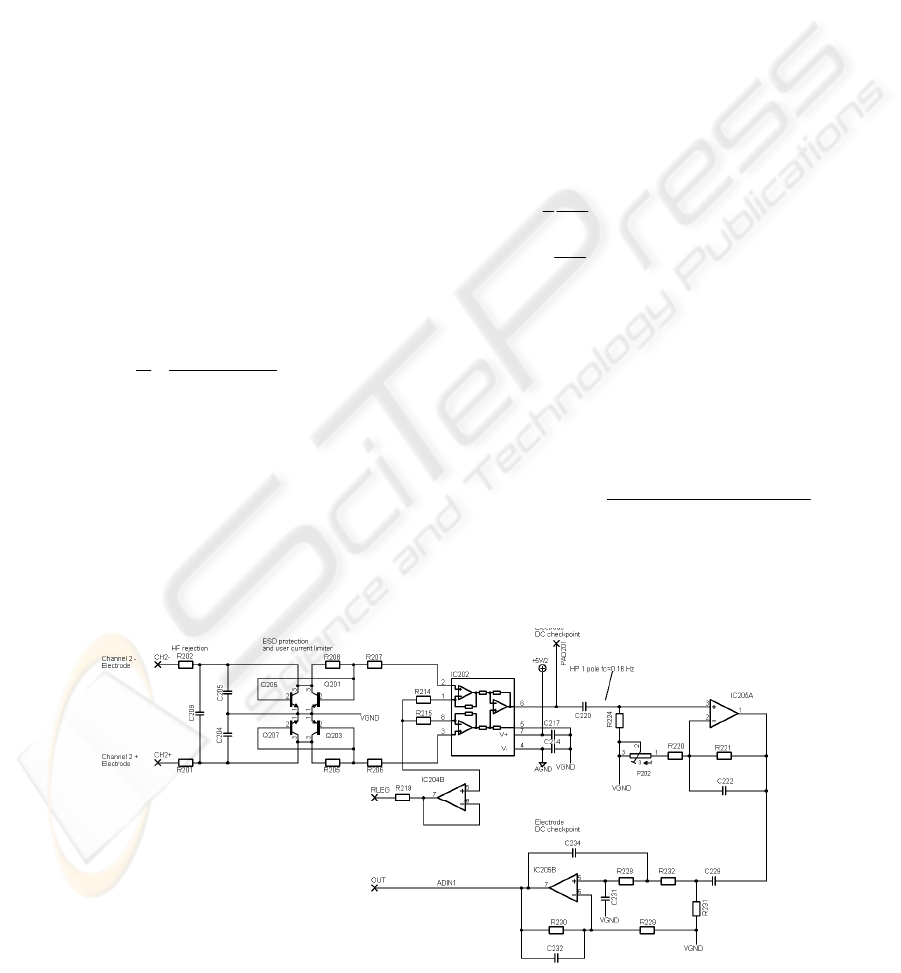
3 RESULTS
The configuration has been adopted both in a
commercial wearable polygraph, in order to acquire
the ECG signal and on a EEG acquisition prototype
devoted to Brain Computer Interface applications.
Figure 8 shows the proposed implementation for the
EEG acquisition device. The system is 3,3V single
supply powered using a li-ion battery and a low-
dropout linear voltage regulator. The
preamplification stage has a gain of 100V/V and
P(s) is realized using a INA118 (Texas Instruments).
The other four operational amplifiers are contained
in a single integrated circuit (TLC2254, Texas
Instruments).
The F(s) is an inverting double pole low pass
filter, and A(s) is an amplification chain. The I(s) is
composed by and attenuation network (R30 and
R31), an inverting integrator (IC2B, C1 and R12)
and the nonlinear activation network (K2, H2, R22,
R23, R25, R27, R26).
The R27 and R26 network are used in order to
set the intervention threshold of the offset recovery
circuit: when the V
be
of K2 and H2 are kept below
0,7 Volt the transistor are turned off. The Th
parameter is defined also follows:
27
2627
7,0
R
RR
VTh
+
⋅=
(6)
K2 is switched on when the amplifier output voltage
reaches the upper saturation limit, while H2 is
switched on in case of lower saturation. When one
of the transistor is turned on, it injects a current into
the inverting integrator causing the fast offset
recovery. R22, R23, R25 are necessary in order to
limit the transistor current and avoid instabilities
related to 2
nd
order effects of the components. The
final amplification stage is optional an provides a
last anti aliasing filtering.
The system circuit has been successfully used in a
brain computer interface application (Piccini, 2005
and Maggi, 2006) and has an offset recovery time of
less than 10ms.
4 DISCUSSION
The proposed architecture is a smart and cost
effective solution to the problems related to the
acquisition of biosignal in difficult acquisition
situations based on an analog design; thanks to the
evolution of modern digital devices, it is possible to
adopt other method in order to achieve similar
results.
The strength of the proposed topology is that a
simple local solution doesn’t require a full systemic
redesign and support development of modular
multiparametric wearable devices.
The discussion doesn’t take into account second
order effects related the components physical
limitations: even if the architecture is robust and the
frequency range of biosignals is reduced, the design
of an amplifier based on the proposed topology
should be approached with care.
Figure 8: Schematic of the EEG amplification circuit.
BIOSIGNAL ACQUISITION DEVICE - A Novel Topology for Wearable Signal Acquisition Devices
401

5 CONCLUSIONS
The analysis proposed in this paper shows an
interesting approach for providing a cost effective
solution for AC coupled, low power amplifiers.
Although born in a biomedical research laboratory,
it faces problems related to a wide range of different
applications. Also for this reason, this generic
topology has been patented in Italy, and successfully
revised by the European Patent Office for the PCT
extension.
ACKNOWLEDGEMENTS
This work has been partially supported by ST
Microelectronics and IIT Istituto Italiano di
Tecnologia.
REFERENCES
Park, S., Sundaresan, J., 2003. IEEE Engineering in
medicine and biology magazine, Enhancing the
quality of life trhough wearable technology
Webster J. G., 1991. Innov. Tech. Biol Med. 12, n°spécial
1, pp. 39-45, Noise sources in surfaces electrodes
L.Maggi, L. Piccini, S. Parini, F. Beverina, S. Silvoni, G.
Andreoni, 2004. Biomedizinsche Technik, v.49 pp.69-
70, “A portable electroencephalogram acquisition
system dedicated to the brain computer interfaces”.
L.Piccini, L.Maggi, S.Parini, G.Andreoni, 2005. Shangai,
Proceedings of EMBC. “A Wearable Home BCI
system: preliminary results with SSVEP protocol”.
L. Maggi, S. Parini, L.Piccini, G.Panfili and G.Andreoni,
2006. NY, Proceedings of EMBC. “A four command
BCI system based on the SSVEP protocol.,
BIOSIGNALS 2008 - International Conference on Bio-inspired Systems and Signal Processing
402
