
MPSOC
ARCHITECTURAL DESIGN AND SYNTHESIS FOR
REAL-TIME BIOMEDICAL SIGNAL PROCESSING IN GAMMA
CAMERAS
Kai Sun, Hongxing Wei, Tianmiao Wang
Robot Research Institute, Beihang University, Beijing 100083, China
Meng Wang, Zili Shao
∗
Department of Computing, Hong Kong Polytechnic University, Hung Hom, Kowloon, Hong Kong
Hui Liu
Software Engineering Institute, Xidan University, Xi’an, China
Keywords:
MPSoC, Gamma Camera.
Abstract:
In this paper, we propose an MPSoC architecture for implementing real-time signal processing in gamma
camera. Based on a fully analysis of the characteristics of the application, we design several algorithms to
optimize the systems in terms of processing speed, power consumption, and area costs etc. Two types of
DSP core have been designed for the integral algorithm and the coordinate algorithm, the key parts of signal
processing in a gamma camera. We implement our MPSoC architecture on FPGA, and synthesize DSP cores
and Network-on-Chip using Synopsys Design Compiler with a UMC 0.18um standard cell library. The results
show that our technique can effectively accelerate the processing and satisfy the requirements of real-time
signal processing for 256 × 256 image construction.
1 INTRODUCTION
The growing demand for increasing sophisticated
biodevices requires high-performance processing
techniques. MPSoC (Multi-Processor System-on-
Chip) is an ideal architecture for biomedical applica-
tions with its high throughput. With MPSoC, we can
integrate multiple heterogeneous processors, hierar-
chy memory systems, custom logic, and on-chip inter-
connection to implement complex functions. There-
fore, in the previous work, application-specific MP-
SoC architecture has been studied for biomedical ap-
plications. In (Khatib et al., 2006), a novel MPSoC ar-
chitecture is proposed for real-time ECG (Electrocar-
diogram) analysis. By employing multi-issue VLIW
DSPs with system interconnect from STMicroelec-
tronics and commercial off-the-shelf biomedical sen-
sors, the proposed MPSoC architecture can perform
real-time ECG analysis with high sampling frequen-
cies. In this paper, we propose an MPSoC architecture
to solve real-time digital signal processing for gamma
∗
The
corresponding author.
cameras, most commonly used medical imaging de-
vices in nuclear medicine.
Gamma cameras generate images based on gamma
radiation detection. PMT (PhotoMultiplier Tube) is
one of the key components in a gamma camera which
can detect fluorescent flashes generated by a crystal
and produce current. Then the current and voltage are
converted to digital signals by ADC (Analog to Dig-
ital Converter) behind a PMT, and finally images are
obtained by processing the digital signals. To gen-
erate images, multiple PMTs are placed in hexagon
configurations behind the absorbing crystal. In a typi-
cal scheme, a PMT array may consist of more than 30
PMTs. Using a serial 2D images obtained by gamma
cameras from the different angles, 3D information
can be acquired by SPECT (Single Photon Emission
Computed Tomography).
To accelerate data processing, in current gamma cam-
eras, DSP (Digital Signal Processing) boards based
on PC platforms are widely used. With such plat-
forms, typically, it takes about 15 - 30 seconds to
generate one 64 × 64 image and 15 - 20 minutes to
279
Sun K., Wei H., Wang T., Wang M., Shaoâ
´
L
˚
U Z. and Liu H. (2008).
MPSOC ARCHITECTURAL DESIGN AND SYNTHESIS FOR REAL-TIME BIOMEDICAL SIGNAL PROCESSING IN GAMMA CAMERAS.
In Proceedings of the First International Conference on Biomedical Electronics and Devices, pages 279-284
DOI: 10.5220/0001053802790284
Copyright
c
SciTePress
finish a complete scan in SPEC. The platforms can
not efficiently produce higher-quality images such as
256×256. Their slow processing speed and big size
limit the effective use of gamma cameras. The prob-
lem become particularly severe for portable gamma
cameras (Sanchez et al., 2004; Sanchez et al., 2006)
which work with nuclear radiation detectors with
room-temperature. To improve image construction
speed, a technique called PMT-PSPMT (Position Sen-
sitive PhotoMultiplier Tube) (Jeong et al., 2004) is
proposed. PMT-PSPMT is very effective in optimiz-
ing image construction times. But it reduces the im-
age quality and cannot construct 256 × 256 image
dynamically.
To solve these problems, we propose an MPSoC
architecture for PMT data processing in a gamma
camera. Our MPSoC architecture consists of the
following four parts: one general-purpose embed-
ded processor, a high speed data interface (HSDI),
application-specific DSP cores and a Network-on-
Chip with an interconnection bus. In the paper, we
design two types of DSP core to implement two
key algorithms, integral and coordinate, for real-time
biomedical applications. We implement a prototype
of our MPSoC architecture with FPGA, and synthe-
size DSP cores and Network-on-Chip using Synop-
sys Design Compiler with a UMC 0.18um standard
cell library. The results show that our technique can
effectively accelerate the processing and implement
communication with small area cost. It can satisfy the
requirements of real-time signal processing for 256 ×
256 image construction.
The rest of this paper is organized as follows: in
Section 2, we introduce necessary backgrounds re-
lated to gamma camera technique. In Section 3, we
present the MPSoC system design. Section 4 presents
the implementation of the prototype system. Sec-
tion 5 provides the experimental results and discus-
sions. In Section 6, we conclude the paper.
2 BACKGROUND
In this section, we provide an overview of basic
knowledge related to gamma cameras. We first intro-
duce the basic operating mechanism of gamma cam-
eras and then present the algorithms used for image
processing.
2.1 The Mechanism of Gamma
Cameras
A gamma camera is a commonly used medical imag-
ing device in nuclear medicine. In a gamma camera,
images are generated by detecting gamma radiation.
Basically, the counts of gamma photons that are ab-
sorbed by a crystal are accumulated, and the crystal
produces a faint flash of light at the same time. The
PMT array behind the crystal detects the fluorescent
flashes and generates current. The current signal gen-
erated by the PMT is captured by the ADC, and two
corresponding voltage signals are converted into dig-
ital signals. Digital signals are used to calculate the
coordinate and energy of the gamma photons. With
these coordinate and energy data, the final image can
be produced.
2.2 Image-Construction Algorithms in
Gamma Camera
During the whole medical imaging procedure, three
algorithms, the integral, coordinate and amendment
algorithms, are applied to the collected data.
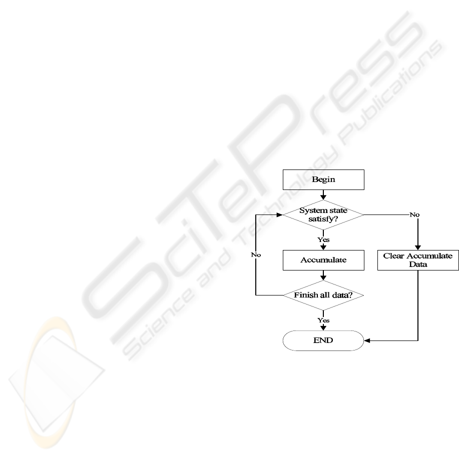
The integral algorithm, as shown in Figure 1, is
to calculate the energy of the voltage signal. In this
algorithm, the serial data of each PMT is accumulated
based on system status conditions.
Figure 1: The integral algorithm.
The coordinate algorithm, as shown in Algorithm 2.1,
includes the calculation for two parts, position and en-
ergy. In this algorithm, P
1
, P
2
···P
m
and N
1
, N
2
···N
m
are the internal data obtained from the two voltage
signals, m is the count of the PMTs, and T
1
, T
2
···T
m
and R
1
, R
2
···R
m
are constant numbers. With these
position and energy data, the gamma photon pulse can
be determined. Then, an image can be constructed
with a serial of the gamma photon pulse.
The amendment algorithm is used to amend energy
BIODEVICES 2008 - International Conference on Biomedical Electronics and Devices
280

Algorithm 2.1 The Coordinate Algorithm.
Require: P
1
, P
2
···P
m
,{ the internal data from the
two voltage signal, m is the count of the PMTs}
N
1
, N
2
···N
m
, { the internal data from the two
voltage signals, m is the count of the PMTs}
T
1
, T
2
···T
m
,{ constant numbers}
R
1
, R
2
···R
m
,{ constant numbers}
1: X
p
⇐
∑
m
i=1
(P
i
×T
i
)
∑
m
i=1
P
i
, Y
p
⇐
∑
m
i=1
(P
i
×R
i
)
∑
m
i=1
P
i
, X
n
⇐
∑
m
i=1
(N
i
×T
i
)
∑
m
i=1
N
i
, Y
n
⇐
∑
m
i=1
(N
i
×R
i
)
∑
m
i=1
N
i
2: calculate the position: x ⇐
(X
p
−X
n
)
(X
p
+X
n
)
, y ⇐
(Y
p
−Y
n
)
(Y
p
+Y
n
)
3: calculate the energy: E ⇐
∑
m
i=1
P
i
+
∑
m
i=1
N
i
and position data with three table-lookup operations.
This algorithm consists of two parts, energy and lin-
earity emendation. After the data of every pulse is
corrected by the correction table, a two-dimensional
image of the relative spatial count density is con-
structed. With more pulse data, we can obtain more
accurate image. To achieve that, multiple PMTs are
placed in a hexagon array. In practical, a typical
scheme usually uses 37 PMTs. The frequency of the
pulse is limited to 1KHz in a typical gamma camera
in order not to keep pulse data. Thus, with such a
gamma camera, it takes about 15-30 seconds to build
up one 64 × 64 image.
To reduce the image construction time, we can in-
crease the pulse frequency of gamma photons. But
with the limitation of the device, the maximum pulse
frequency currently we can achieve is 500KHz-1
MHz. Correspondingly, we have to improve the speed
of digital signal processing in order to generate im-
age with such high pulse frequency. In this paper, our
goal is to design an MPSoC architecture that can gen-
erate one 256 × 256 image in less than one second for
gamma cameras with 1 MHz pulse frequency.
3 MPSOC SYSTEM DESIGN
In this section, we first introduce the MPSoC archi-
tecture in Section 3.1. Then we present issues related
to general processors and HSDI in Section 3.2 and
Section 3.3, respectively. Finally, the design of DSP
cores and interconnection synthesis are discussed in
Section 3.4 and Section 3.5, respectively.
3.1 Architecture Overview
Our MPSoC architecture is a typical heterogeneous
multi-core architecture targeting on the application of
gamma camera. It is specially designed for process-
ing PMT data in parallel with multi-processors. In
practice, fast image processing speed and high-quality
image are the two of the most important performance
metrics for gamma cameras. In order to achieve these
goals, an MPSoC architecture, as shown in Figure 2
is proposed to speed up the image generation and im-
prove image quality.
As shown in Figure 2, our MPSoC architecture
consists of four parts: general processor, HSDI (High
Speed Data Interface), DSP, and interconnection syn-
thesis. Besides the four key parts, the MPSoC archi-
tecture also consists other components, e.g., the gen-
eral embedded micro-controllers. In this architecture,
the processor speed and the 32-bit on-chip intercon-
nection are 200MHz, which are compatible with the
0.18um ASIC technology and the 32-bit bus interface
IP cores. Next, we present the design issues for each
key part of MPSoC architecture.
3.2 The General Processor
The general processor has one general purpose pro-
cessor and some necessary IP cores, such as timer,
UART, and SPI etc. Among these IP cores, the
most important components are the on-chip RAM,
SRAM/Flash controller, SDRAM controller and Eth-
ernet MAC controller. The amendment algorithm and
other general purpose computing are implemented in
the general processor. The SRAM/Flash controller
provides an interface to SRAM, ROM, NOR Flash
and NAND Flash. The instruction code is stored in
NOR Flash which is boot memory of the general pro-
cessor. A reliable file system that stores the config-
urations using in the amendment algorithm is imple-
mented in the NAND Flash. With an external Ether-
net PHY chip, the Ethernet MAC controller is used
to establish the communications with remote comput-
ers. In this way, the images and videos can be trans-
ferred to the remote computers through network, thus
to help the doctors do some diagnosis. The on-chip
RAM capacity is 512KB with 5 partitions. The first
2 partitions contain two amendment tables which are
256 × 256 × 16 bit. The third partition contains one
256 × 256 × 8 bit amendment table. The fourth par-
tition contains the image constructed, which is 256
pixel × 256 pixel × 16 bit. The last partition is used
as a high speed memory.
3.3 The High Speed Data Interface
(HSDI)
The HSDI has a PMT data buffer and several LVDS
(Low Voltage Differential Signaling) interfaces which
MPSOC ARCHITECTURAL DESIGN AND SYNTHESIS FOR REAL-TIME BIOMEDICAL SIGNAL PROCESSING
IN GAMMA CAMERAS
281
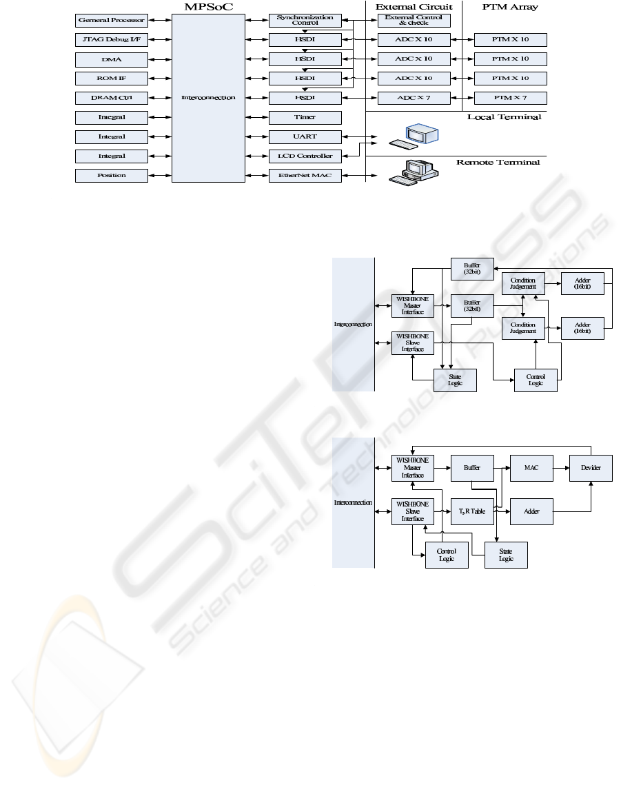
Figure 2: The MPSoC Architecture.
build a connection with external high speed ADCs.
Since the sample speed of the ADC for PMTs is far
lower than the processing time, buffers are used to
store the PMT data of the external ADC. To exert the
processing capability and diminish the interconnec-
tion area, the mount of the HSDI is determined by two
factors: 1) the ADC sample speed; and 2) the on-chip
interconnection speed. Usually, the common sample
speed of the ADC for PMTs is 30MHz with the data
width less than 16 bit, and the typical processor speed
and on-chip interconnection with 0.18um technology
and 32 bit width are 200MHz. Considering the bus
arbitration cost, the maximum capacity of one HSDI
is to take charge on 11 ADC data channels. For all of
the 37 ADC data channels as discussed above, we use
4 HSDI as shown in Figure ??(a) in which 3 of them
take charge of 10 ADC data channels, and the last one
takes charge of 7 ADC data channels.
3.4 The DSP Core Design
The customized DSPs used in our MPSoC architec-
ture are designed for implementing the integral al-
gorithm and the coordinate algorithm. We design
two types of DSP, integral and coordinate, to imple-
ment the integral and coordinate algorithm, respec-
tively. The corresponding block diagrams of the inte-
gral DSP and coordinate DSP are shown in Figure 3
and Figure 4, respectively.
The integral DSP has two bus interfaces, Master
and Slave. The Master interface implements the data
load/store, and the Slave interface implements the
control and status logic accessing from other devices.
The parameters for the integral algorithm are obtained
through the Slave interface. Since there are 60 16-bit
data for every gamma photons with two groups, upper
and lower, which are implemented in the same inte-
gral algorithm, the data from HSDI is placed into the
Figure 3: The Integral DSP.
Figure 4: The Coordinate DSP.
buffer with 32-bit format, 16-bit for the upper group
and 16-bit for the lower group. In other words, the
integral algorithm is processed in parallel in the in-
tegral DSP. Thus, the integral DSP is designed with
same units to accelerate the processing speed. For 30
PMTs data, the integral DSP uses 36 cycles to pro-
cess them in which each integral DSP processes 10
gamma photons pulses within 2us. Thus, 4 integral
processors are needed to process all of the 37 channel
PMTs data.
The block diagram of the coordinate DSP is
shown in Figure 4. The main components of the coor-
dinate DSP are MAC (Multiply Accumulate) and Di-
vider. The coordinate DSP has two bus interfaces,
Master and Slave, which are as same as those of the
BIODEVICES 2008 - International Conference on Biomedical Electronics and Devices
282
integral DSP. The T and R parameter tables are ac-
cessed through the Slave interface, and the data to be
processed is placed in the buffer through the Master
interface. As the MAC and Adder can work in par-
allel, we can process the numerator and denominator
in algorithm 2.1 simultaneously. Since the throughput
of the coordinate algorithm is much lower than the in-
tegral algorithm, only one coordinate DSP is required
in the DSP design.
3.5 Interconnection Synthesis
As shown in Figure 2, interconnection serves
the communication among DSP cores and other
components. In most on-chip bus standards,
such as AMBA(SPE, 2001), CoreConnect(SPE, ),
STBus(SPE, 2003) and WISHBONE(SPE, 2002), a
share structure is used in the embedded processor. In
the structure, the total bandwidth of the interconnec-
tion is limited to the bandwidth of each node since all
buses are connected to one node and only one master
can access the interconnection at one time. In order
to fully utilize bandwidth, we need to perform careful
analysis. In (Wang et al., 2007), we propose an inter-
connection synthesis algorithm to solve the problem.
4 PROTOTYPE
IMPLEMENTATION
We have implemented the MPSoC prototype in an Al-
tera Cyclone II FPGA EP2C35F672. In the imple-
mentation, we use the OpenRisc 1200 processor core
as the general processor that runs at 20MHz which is
10% of the speed of the final ASIC implementation.
We add one 512KB ZBT SRAM to our prototype
since the on-chip RAM in Cyclone II FPGA can not
meet our requirements. Besides the external SRAM,
the prototype has 64MB SDRAM, 32MB NOR Flash
ROM, 128MB NAND Flash ROM, 10M/100M Ether-
net PHY, 640 × 480 16bit TFT LCD and other chips.
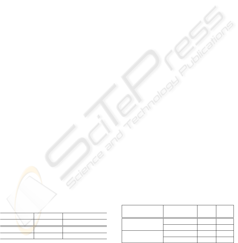
Table 1: The information for the prototype.
LEs RAM(KB) Multiplier(9-bit)
23468 (71%) 54 (92%) 16 (23%)
IO PLL Max Speed(MHz)
465 (98%) 1 (25%) 42
We test the prototype with input signals based on
a real gamma camera, and check the output signals.
The results show that it functions correctly. The num-
bers of resources we use are shown in Table 1. In
this table, LEs denotes logical elements, RAM rep-
resents the on-chip-memory, and PLL denotes phase
loop lock. The number inside the brackets for each
resource represents the percentage between the num-
ber of resource we really use and the total number of
resource provided by the system.
5 EXPERIMENTAL RESULTS
AND DISCUSSIONS
To compare our MPSoC architecture with the general
architecture, we have implemented the integral and
coordinate algorithm both with an ARM9 processor
and with our custom designed DSPs. In the exper-
iment, we obtain the results of processing time, the
area, RAM, power cost of our custom DSPs. For the
interconnection, we have implemented our intercon-
nection with WISHBONE protocol and our bus in-
terconnection synthesis algorithm. We compare our
technique with the crossbar and the reduce crossbar
structure in terms of the area cost. In this section,
we first present the results of processor comparison
in Section 5.1, and then we present and analyze the
results of interconnection optimization in Section ??.
5.1 Processor Comparison
The typical sustaining time of the PMT reactivity
electric current signal for gamma photons pulse is
2us. In this time interval, the ADC produces 60 data
in which every 30 data is applied with the integral
algorithm. The cycles and time for the integral and
coordinate algorithm to process data that is produced
within 2us are shown in table 2. We have tested the
ARM9 program in SimpleScalar (Burger and Austin,
1997) and a hardware platform based on ARM 920T
(ARM 920T, 2001) running with 203 MHz. The re-
sults are shown in Table 2.
Table 2: The testing results of ARM9 program in Sim-
pleScalar and S3C2410.
Condition Cycle Time
(us)
The Integral SimpleScalar 2104 10.5
Algorithm S3C2410 21.6
The Coordinate SimpleScalar 1692 8.5
Algorithm S3C2410 24.2
In the table, we can see that it takes 2104 and 1692
clock cycles to finish the integral and coordinate al-
gorithms, respectively, on the SimpleScalar simulator.
MPSOC ARCHITECTURAL DESIGN AND SYNTHESIS FOR REAL-TIME BIOMEDICAL SIGNAL PROCESSING
IN GAMMA CAMERAS
283
Based on the hardware platform, the times we need
are 21.6 and 24.2 µs, respectively.
We design two types of DSP to implement the al-
gorithms separately. In order to accelerate the pro-
cessing speed, we use several integral DSPs with
same design. The integral and coordinate DSPs are
coded in Verilog HDL, and are synthesized to gate-
level circuits using Synopsys Design Compiler and a
UMC 0.18um standard cell library. The results gener-
ated by our technique is shown in Table 3. The com-
parison of the results generated using ARM9 and our
customized DSP is shown in Table 4. From the ta-
ble, we can see that our customized DSPs can pre-
form with very high performance. With 5 integral
DSP cores, we can achieve the requirements. The re-
sults show great performance improvement and cost
reduction with our MPSoC architecture.
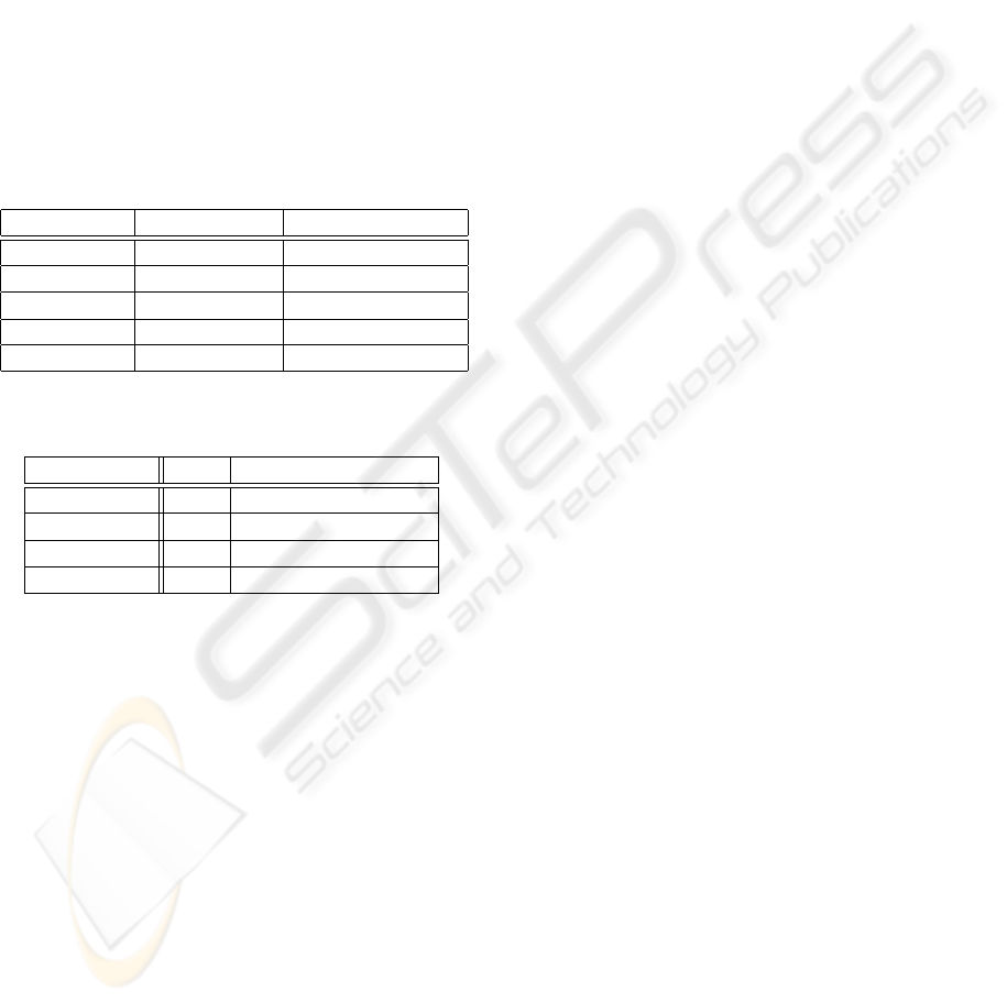
Table 3: The results with our DSP cores.
Integral DSP Coordinate DSP
Cycle 37 340
Time(us) 0.185 1.700
Area(um
2
) 0.14 2.03
RAM(KB) 1 4
Power(mW) 18 264
Table 4: The comparison of the results from ARM9 and our
DSP cores.
DSP ARM920 Processor
Quantity 5 197
Area(um
2
) 2.59 1026.8
RAM(KB) 8 3152
Power(mW) 336 120
6 CONCLUSIONS
In this paper, we have proposed an MPSoC architec-
ture for implementing real-time signal processing in
gamma camera. Based on a fully analysis of the char-
acteristics of the application, we designed several al-
gorithms to optimize the systems in terms of process-
ing speed, power consumption, and area costs etc.
Two types of DSP core have been designed for the
integral algorithm and the coordinate algorithm, the
key parts of signal processing in a gamma camera.
A prototype of our MPSoC architecture has been im-
plemented with FPGA, and the test results show that
it can function correctly. Various experiments have
been conducted and discussed. We synthesized DSP
cores and Network-on-Chip using Synopsys Design
Compiler with a UMC 0.18um standard cell library.
The results show that our technique can effectively
accelerate the processing and satisfy the requirements
of real-time signal processing for 256 × 256 image
construction.
ACKNOWLEDGEMENTS
The work described in this paper was partially sup-
ported by the grants from the Research Grants Coun-
cil of the Hong Kong Special Administrative Region,
China (PolyU A-PH13, PolyU A-PA5X, PolyU A-
PH41, and PolyU B-Q06B), the National Nature Sci-
ence Foundation of China (60525314), the 973 Pro-
gram of China (2002CB312204-04) and the 863 Pro-
gram of China (2006AA04Z206).
REFERENCES
Ibm on-chip coreconnect bus architecture.
www.chips.ibm.com.
(2001). Arm amba specification (rev2.0). www.arm.com.
(2002). Wishbone system-on-chip (soc) interconnection
architecture for portable ip cores revision: B.3.
www.opencores.org.
(2003). Stbus communication system: Concepts and defini-
tions, reference guide. STMicroelectronics.
ARM 920T, R. . (2001). Technical Reference Manual.
Burger, D. and Austin, T. M. (1997). The simplescalar tool
set, version 2.0. SIGARCH Comput. Archit. News,
25(3):13–25.
Jeong, M. H., Choi, Y., Chung, Y. H., Song, T. Y., Jung,
J. H., Hong, K. J., Min, B. J., Choe, Y. S., Lee, K.-H.,
and Kim, B.-T. (2004). Performance improvement of
small gamma camera using nai(tl) plate and position
sensitive photo-multiplier tubes. Physics in Medicine
and Biology, 49(21):4961–4970.
Khatib, I. A., Poletti, F., Bertozzi, D., Benini, L., Bechara,
M., Khalifeh, H., Jantsch, A., and Nabiev, R.
(2006). A multiprocessor system-on-chip for real-
time biomedical monitoring and analysis: architec-
tural design space exploration. In DAC, pages 125–
130.
Sanchez, F., Benlloch, J. M., Escat, B., Pavon, N., Porras,
E., Kadi-Hanifi, D., Ruiz, J. A., Mora, F. J., and Se-
bastia, A. (2004). Design and tests of a portable mini
gamma camera. Medical Physics, pages 1384–1397.
Sanchez, F., Fernandez, M. M., Gimenez, M., J.M., J. M. B.,
Rodriguez-Alvarez, M. J., Quiros, F. G. D., Lerche,
C. W., Pavon, N., Palazon, J. A., Martinez, J., and Se-
bastia, A. (2006). Performance tests of two portable
mini gamma cameras for medical applications. Medi-
cal Physics, pages 4210–4220.
Wang, T., Sun, K., Wei, H., Wang, M., Shao, Z., and Liu,
H. (2007). Interconnection synthesis of mpsoc archi-
tecture for gamma cameras. In EUC.
BIODEVICES 2008 - International Conference on Biomedical Electronics and Devices
284
