
Surface Plasmon Devices for Nanoscale Integration with Electronic
Device on Silicon
Optical Signal Transmission and Detection through Surface Plasmon
on Nanoscale Circuit
M. Fukuda, T. Aihara, M. Fukuhara, A. Takeda, Y. Ishii, and T. Ishiyama
Electrical and Electronic Information Engineering, Toyohashi University of Technology, 1-1 Hibarigaoka,
Tempakucho, Toyohashi, Aichi, Japan
Keywords: Surface Plasmon, Integrated Circuit, Signal Transmission, Silicon, Electronic Device.
Abstract: This paper discusses the architecture of surface plasmon devices for silicon-based nanoscale-integrated
circuits. A suitable structure for surface plasmon devices integrated monolithically with electronic devices is
described based on surface plasmon devices fabricated in our group. These devices were fabricated on
silicon with conventional CMOS processes. In the devices, light-wave signals are converted into surface
plasmon signals with a grating and detected with a Schottky-type diode on a silicon substrate. Both intensity
and frequency signals are transmitted along the surface plasmon waveguide in the nanoscale circuit. Such
signals were easily amplified with MOSFETs integrated monolithically on the silicon substrate. Here, the
wavelength of light used in the circuit is set within the 1550-nm-wavelength band to prevent signals
absorption by silicon. This can lead to a simpler structure for waveguides and devices on silicon substrates.
These techniques and devices will open a new phase for surface plasmon circuits integrated with electronic
devices on silicon substrates.
1 INTRODUCTION
Daily communications are increasingly maintained
and supported by optical fibre transmission systems.
One of the key components in systems is the
electronic device integrated circuit (IC). The
progress of such ICs is now, however, saturated
because the integration density is approaching scale
limits and the signal transmission rate is limited by
the wire delay on the silicon substrate. Power
dissipation and heat generation are also serious
problems. To solve these problems, an optical
interconnect has been trialled in ICs. Optical
interconnects can eliminate wire delay and heat
generation, subsequently, several devices have been
developed and proposed in the field of silicon
photonics. Here, there is a real possibility that the
scale of the interconnect can be further reduced if
surface plasmons can be used as signal carriers
instead of light.
Recently, various photonic devices using surface
plasmons have been developed for many
applications (Yatsui et al., 2001; Maier et al., 2002;
Nikolajsen et al, 2003; Barnes et al., 2003;
Boltasseva et al., 2005). Transmission waveguides
(Sergey et al., 2006; Ebbesen st al., 2008; Kim et al.,
2008; Verhagen et al., 2009; Aihara et al., 2012)
have been developed for signal transmission using
surface plasmons. These waveguides are basically
thin metal films, but the challenge is to increase the
propagation distance of surface plasmons. Long-
distant propagation, however, is more difficult for
surface plasmons than for propagating light
(Boltasseva et al., 2005).
Optical detectors using surface plasmon
resonance have also been developed in various
wavelength ranges. Some detectors using Schottky
barriers were studied and developed in the
wavelength range transparent to silicon (Akbari et
al., 2010; Fukuda et al., 2010; Casalino et al., 2010;
Aihara et al., 2011; Goykham et al., 2012; Hashemi
et al., 2013). There is, however, no report on surface
plasmon ICs integrated with electronic devices.
In this paper, surface plasmon devices developed
in our group are discussed in regard to integrating
with electronic devices on a silicon substrate. The
surface plasmon devices in our focus are waveguides,
152
Fukuda M., Aihara T., Fukuhara M., Takeda A., Ishii Y. and Ishiyama T..
Surface Plasmon Devices for Nanoscale Integration with Electronic Device on Silicon - Optical Signal Transmission and Detection through Surface
Plasmon on Nanoscale Circuit .
DOI: 10.5220/0004680501520157
In Proceedings of 2nd International Conference on Photonics, Optics and Laser Technology (PHOTOPTICS-2014), pages 152-157
ISBN: 978-989-758-008-6
Copyright
c
2014 SCITEPRESS (Science and Technology Publications, Lda.)
surface plasmon (light) detectors, and the IC of
asurface plasmon detector and MOSFET (Fukuda et
al., 2007; Fukuda et al., 2008; Fukuda et al., 2010;
Aihara et al., 2011; Fukuhara et al., 2012; Aihara et
al., 2012; Aihara et al., 2013; Takeda et al., 2013).
The points of discussion are the basic architectures
and suitable structures that need to be clarified and
proposed for monolithic integration with electronic
devices. The basic structure of detectors and
waveguides and device integration architectures are
discussed in section 2. Device performance and
feasibility of integration are presented in section 3.
The results are summarized in secton 4.
2 DEVICE INTEGRATION AND
ARCHITECTURES
A few factors are important for integrating surface
plasmon devices with electronic devices and for
merging both types of device on silicon substrates.
The factors relevant for surface plasmon devices are:
(1) simple structure and process,
(2) materials: metal and silicon/silicon oxide,
(3) light transparent to silicon,
(4) short signal transmission distance of order below
a few hundred nanometres.
To integrate easily surface plasmon devices with
electronic devices on silicon, the surface plasmon
devices have to be fabricated using silicon/silicon
oxide. The wavelength transparent to silicon are,
therefore, favoured as signal carrier waves.
Moreover, silicon ICs operate with electrons, and
thus signal-carrying light must be converted into
electronic signals using silicon photonic devices. In
addition, the signals are transmitted along a metal
film without any optical waveguide. This structure
can control an optical signal using surface plasmons.
Simple structures and processes are also important to
integrate them on a silicon substrate.
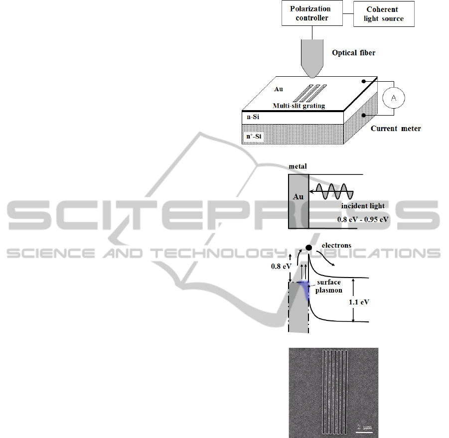
2.1 Optical / Surface Plasmon Detector
Based on the device architecture just described, we
have developed a silicon-based photodetector that
monitors optical signals in the wavelength range
transparent to silicon. Two types of photodetector,
nanoparticle (Fukuda et al., 2010) and grating
(Aihara et al., 2011) were developed for this purpose.
For our ICs, though, a grating-type photodetector
was selected because of its efficiency and process
controllability. The basic device structure and
operating mechanism are shown in Figure 1.
(a) schematic diagram.
(b) band diagram.
(c) SEM image of a multi-slit grating.
Figure 1: Grating-type surface plasmon detector
(photodiode) with a Au/silicon Schottky barrier.
A thin gold film of about a few hundred
nanometers was deposited on a silicon substrate, and
then grating slits (the width: 150 nm and the pitch:
440 nm for 1550-nm-wavelength light) were
fabricated using focused ion-beam etching. At the
interface between the gold film and silicon, excited
electrons can flow over the barrier when propagating
light is incident on the grating. The photocurrent, I
p
,
is proportional to the square of the energy difference
between the incident light and the barrier height as
expressed by (Mead and Spitzer, 1963),
SurfacePlasmonDevicesforNanoscaleIntegrationwithElectronicDeviceonSilicon-OpticalSignalTransmissionand
DetectionthroughSurfacePlasmononNanoscaleCircuit
153
I
p
= A (h –
B
)
2
(1)
where A is a constant of proportionality, h is the
Planck’s constant, is the incident light frequency,
and
B
is the Schottky barrier height. Light of any
wavelength is therefore detected if h is greater than
B
, even if it is transparent to the semiconductor. If
the polarization direction of the incident light is in
the direction perpendicular to the slits (TM), surface
plasmons are excited in the gold film and the amount
of electrons crossing over the barrier increases
markedly (see Figure 2). This structure can therefore
be used as a detector of light and surface plasmons
in the wavelength range transparent to silicon.
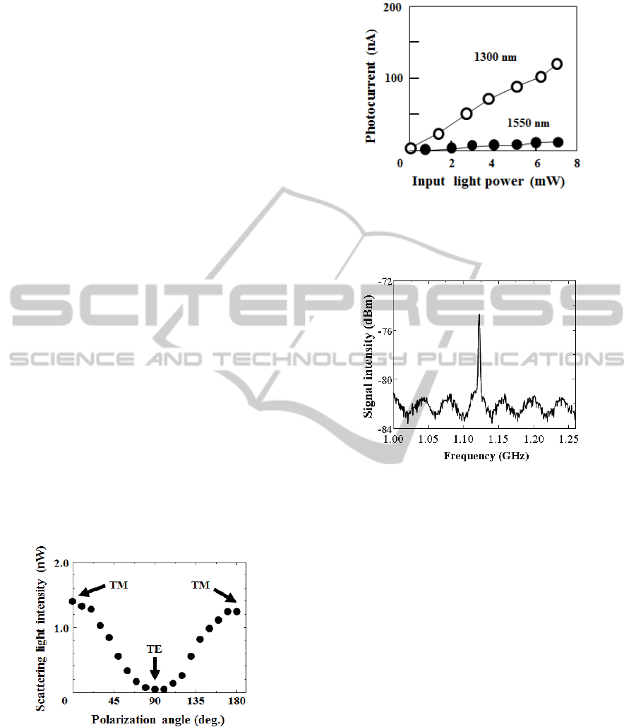
Although the efficiency depends on the wavelength
of incident light (see Figure 3), the detector can
convert light, and thus surface plasmons, into a
photocurrent (or electron flow) of wavelengths
roughly below 1600 nm (Fukuda et al., 2010). This
range can cover wavelengths used in optical fibre
transmission systems. Such detectors can monitor
intensity signals as well as frequency signals
transmitted by propagating light/surface plasmon.
When two light beams having a slightly different
frequency (or wavelength) were simultaneously
incident on the slits, the beat signal of the two light
beams (Figure 4) was monitored with the
photodetector using the heterodyne detection
technique.
The performance of light and surface plasmon
detectors can be improved by introducing suitable
structures to the grating (Takeda et al., 2013; Aihara
et al., 2013).
Figure 2: Polarization dependence of the photocurrent in a
light and surface plasmon detector. TM and TE indicate
the incident light polarization, i.e. perpendicular and
parallel respectively to the slit. The polarization angle at 0
degree is set at the polarization perpendicular to the slit
(TM).
Figure 3: Wavelength dependence of the photocurrent in a
gold thin film/silicon Schottky barrier. The conversion rate
was about 17 nA/mW for 1300 nm and 1.7 nA/mW for
1550 nm.
Figure 4: Beat signal detected with the photodetector.
2.2 Surface Plasmon Waveguide
To interconnect surface plasmon and electronic
devices and to transmit signals, surface plasmon
waveguides are indispensable. The target distance
for signal transmission is less than a few hundred
nanometres; if greater transmission distances are
required, propagating light should be used because
the propagating loss of surface plasmon is quite
large.
Waveguide structures are essentially divided into
two types depending on the type of surface plasmon,
propagating or localized. Both types of waveguide
could transmit optical intensity and frequency
signals. These waveguides are described and
discussed in this sub-section.
2.2.1 Propagating Surface Plasmons
This type of surface plasmon propagates along a
continuous metal film at a speed determined by the
dielectric constant of the medium. The transmission
property enables the propagation of surface plasmon
to be controlled with a simple waveguide structure
PHOTOPTICS2014-InternationalConferenceonPhotonics,OpticsandLaserTechnology
154
deposited on the silicon substrate. This is a big
advantage when compared with that of propagating
light which requires a complicated waveguide
structure.
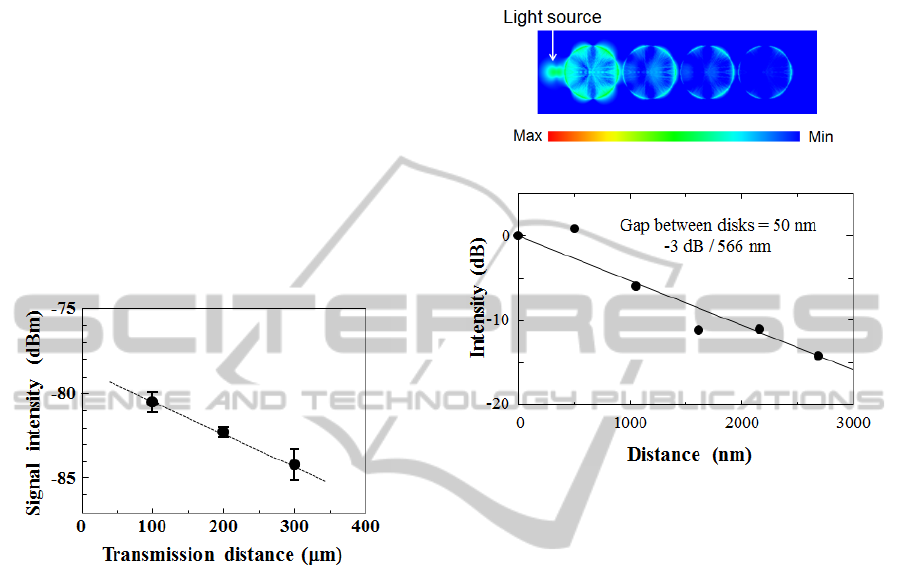
The transmitting length closely depends on the
structure and material of the metal film. The
transmission loss, caused by electron scattering in
metal (Ohmic loss), can be large (see Figure 5)
(Aihara et al., 2012). The transmission loss is,
however, acceptable if the distance is less than a few
hundred nanometres. This transmission distance will
be sufficient to interconnect plasmonic and
electronic devices. Although the quality and
structure of the metal film strongly influences the
transmission loss, the metal waveguide can be easily
fabricated on a silicon wafer without any special
equipment.
Figure 5: Loss characteristics of surface plasmons during
transmission on gold film.
2.2.2 Localized Surface Plasmons
The waveguides for this type of surface plasmon are
not continuous metal films but chains of metal disks
spaced a few ten nanometres. This structure is
useful as it electrically disconnects the IC, although
the loss is much larger than that of a continuous
metal waveguide. The surface plasmon at a disk can
induce surface plasmon resonances at the
neighbouring disk if the chain is set to operate at a
frequency of the surface plasmon resonance. This
behaviour can be continuously transmitted along the
chain, and a signal can be transmitted.
The chain of disks was designed specifically as a
waveguide for localized surface plasmons. Its
transmission loss was estimated using the finite-
different time-domain (FDTD) method; see Figure 6
(Fukuhara et al., 2012). Each disk is gold film with
500-nm in diameter and 100-nm thick; the
separation between disks is set at 50 nm. A light
source of wavelength of 1500 nm is set near the first
disk of the chain. A localized surface plasmon is
induced at the first disk which is then transmitted to
the adjacent disk. Thus, this structure is able to
transmit optical signals converted from incident light
by surface plasmons.
(a) Calculation model.
(b) Intensity change as a function of distance.
Figure 6: Calculation result of intensity variation during
surface plasmon transmission on a chain of nanoscale gold
disks.
2.2.3 Signal Transmission through Surface
Plasmons
Intensity signal transmission has been confirmed on
both the continuous-metal and chain-type
waveguides (Fukuhara et al., 2012; Aihara et al.,
2012). The transmission distance for both is limited
by Ohmic loss. An optical frequency signal was also
transmitted along the continuous gold film without
any coherence degradation (Aihara et al., 2012). For
a chain of disks, the transmission of an optical
frequency signal was estimated using FDTD
simulation. From these results, it can be said that the
intensity and frequency signals are transmitted
through surface plasmons over a nanoscale surface
plasmon circuit on a silicon substrate.
As described, the surface plasmon is controlled
with a simple metal waveguide after conversion
from propagating light. This controllability is
enabled using silicon’s transparency range to light.
SurfacePlasmonDevicesforNanoscaleIntegrationwithElectronicDeviceonSilicon-OpticalSignalTransmissionand
DetectionthroughSurfacePlasmononNanoscaleCircuit
155

3 DEVICE INTEGRATION
Based on the architecture discussed in section 2, a
part of the devices developed was monolithically
integrated with electronic devices onto silicon
substrates. One example is shown in Figure 7
(Aihara et al., 2013). The surface plasmon (or light)
detector is set on the gate electrode of a MOSFET.
This surface plasmon detector and two MOSFETs
IC operated well under DC- and AC-bias, and a
photocurrent converted from incident light through
surface plasmons was electrically amplified.
(a) optical micrograph of the top view.
(b) circuit diagram.
Figure 7: An integrated circuit of a surface plasmon
detector and two MOSFETs.
4 CONCLUSIONS
Using architectures for surface plasmon devices
developed in our group, some suitable structures of
surface plasmon devices have been discussed for
monolithic integration with electronic devices on a
silicon substrate. In the devices, surface plasmons
transparent to silicon were used to prevent
absorption by silicon, and the use of transparent light
with metal waveguides enables easy control of these
surface plasmons. These techniques allow
integration of surface plasmon devices with
electronic devices using standard CMOS process.
The device integration opens a new phase for
nanoscale surface plasmon ICs.
ACKNOWLEDGEMENTS
This study was partially supported by JSPS
KAKENHI Grant Numbers 22360142, 25630147.
REFERENCES
Aihara, T, Nakagawa, K. Fukuhara, M, Yu, Y. L,
Yamaguchi, K, Fukuda, M. (2011) Optical frequency
signal detection through surface plsmon polaritons.
Appl. Phys. Lett. 99, 043111-1-043000-3.
Aihara, T, Fukuda. M. (2012) Observation of plasmonic
frequency-modulated signal transmission. In IEEE
Optical MEMS & Nanophotonics 2012 (65) Alberta,
Canada. IEEE.
Aihara, T, Fukuda. M. (2012) Transmission properties of
surface-plsmon-polariton coherence. Appl. Phys. Lett.
100, 213115-1-213115-4.
Aihara, T, Fukuhara, M, Takeda, A, Futagawa, M, ¿??,
Sawada, K. Fukuda, M. (2013) Monolithic Integration
of surface plasmon detector and metal-oxide-
semiconductor field-effect transistors. IEEE Photonics
J. 5, 6800609.
Akbari, A, Tait, R. N, Berini, P. (2010) Surface plasmon
waveguide Schottky detector. Opt. Express 18, 8505-
8514.
Barnes, W. L, Dereux, A, Ebbesen, T. W. (2003) Surface
plasmon subwavelength optics. Nature 424, 824–830.
Boltasseva, A, Nikolajsen, T, Leosson, K, Kjaer, K,
Larsen, M. S, Bozhevolnyi, S. I. (2005) Integrated
optical components utilizing long-range surface
plasmon polaritons. J. Lightwave Technol. 23, 413-
422.
Sergey, I, Bozhevolnyi, Valentyn, S, Volkov, Devaux, E,
Laluet, J. –Y, Ebbesen, T. W. (2006) Channel
Plasmon subwavelength waveguide components
including interferometers and ring resonators. Nature
440, 508-511.
Casalino, M, Sirleto, L, Lodice, M, Saffioti, N, Gioffre, M,
Rendina, I, Coppola, G. (2010) Cu/p-Si Schottky
barrier-based near infrared photodetector integrated
with a silicon-on-insulator waveguide. Appl. Phys.
Lett. 96, 241112-1-241112-3.
Ebbesen, T. W, Genet, C, Boshevolnyi, S. I. (2008)
Surface Plasmon circuitry. Phys. Today, May, 44-50.
Fukuda, M, Yamasaki, Y, Oota, N, Utsumi, A. (2007)
Optical near-field generation and detection by using
metal-dielectric film fabricated from silver paste and
spherical fused silica. IEEE Photon. Technol. Lett. 19,
1160-1162.
PHOTOPTICS2014-InternationalConferenceonPhotonics,OpticsandLaserTechnology
156

Fukuda, M, Utsumi, A, Funato, H, Tohyama, M,
Takemoto, N, Yamamoto, S, Yamasaki, Y, Tanabe, T.
(2008) Performance of Random Metal-dielectric film
on optical signal transmission. IEEE Photon. Technol.
Lett. 20, 590-592.
Fukuda, M, Aihara, T, Yamaguchi, K, Ling, Y. Y, Miyaji,
K, Tohyama, M. (2010) Light detection enhanced by
surface plasmon resonance in metal film. Appl. Phys.
Lett. 96, 153107-1-153107-3.
Fukuhara, M, Aihara, T, Ushii, Y., Fukuda, M. (2012)
Optical frequency signal transmission via localized
surface plasmons. In IEEE Photonics Conference 2012
(23- 27) Burlingame. IEEE.
Goykhman, I, Desiatov, B, Khurgin, J, Shappir, J, Levy, U.
(2012) Waveguide based compact silicon Schottky
photodetector with enhances responsivity in the
telecom spectral band. Opt. Express 20, 28594-28602.
Hashemi, M, Farzad, M. H, Mortensen, N. A, Ziao, S.
(2013) Enhance plasmonc light absorption for silicon
Schottky-barrier photodetectors. Plasmoncs 8, 1059-
1064.
Kim, J. T, Ju, J. J, Park, S, Kim, M. –S, Park, S. K, Lee, M.
–H. (2008) Chip-to-chip optical interconnect using
gold long-range surface plasmon polariton waveguides.
Opt. Express 16, 13133-13138.
Maier, S. A, Kik, P. G, Atwater, A. (2002) Observation of
coupled plasmon-polariton modes in Au nanoparticle
chain waveguides of different lengths: Estimation of
waveguide loss. Appl. Phys. Lett. 81, 1714–1716.
Mead, C. A, Spitzer, W. G, (1963) Photoemission from
Au and Cu into CdS . Appl. Phys. Lett., 2, 74-75.
Nikolajsen, T, Leosson, K, Salakhutdinov, I, Bozhevolnyi,
S. I. (2003) Polymer-based surface plasmon-polariton
stripe waveguides at telecommunication wavelengths.
Appl. Phys. Lett. 82, 668–670.
Takeda, A, Aihara, T, Fukuhara, M, Ishii, Y, Fukuda, M.
(2013) Optimal design of photodetector with multi-slit
grating. In IEEE Optical MEMS & Nanophotonics
2013 Kanazawa, Japan. IEEE (accepted).
Verhagen, E, Spasenovic, M, Polman, A, Kuipers, L.
(2009) Nanowire Plasmon excitation by adiabatic
mode transformation. Phys. Rev. Lett. 102, 203904-1-
203904-4.
Yatsui, T, Kourogi, M, Ohtsu, M. (2001) Plasmon
waveguide for optical far/near-field conversion. Appl.
Phys. Lett. 79, 4583–4585.
SurfacePlasmonDevicesforNanoscaleIntegrationwithElectronicDeviceonSilicon-OpticalSignalTransmissionand
DetectionthroughSurfacePlasmononNanoscaleCircuit
157
