
Implementation of a Grating-type Spatial Optical Switch based on
Phase Change Material and its Static Measurement
Xiaomin Wang
1
, Masashi Kuwahara
1
, Hitoshi Kawashima
1
and Hiroyuki Tsuda
2
1
National Institute of Advanced Industrial Science and Technology (AIST), Tsukuba Central 4, Tsukuba, Japan
2
Graduate School of Science and Technology, Keio University, 3-14-1 Hiyoshi, Kohoku-ku, Yokohama-shi, Japan
Keywords: Spatial Optical Switch, Diffraction Grating, Phase Change Material.
Abstract: We have implemented a new grating-type spatial optical reflection switch based on phase change material
(PCM) for usage at optical communication wavelength. This grating device switches on/off the light or
steers the light propagation direction by switching the PCM grating between its amorphous and crystalline
states. Thus, the switching status is non-volatile and the device is promising for power saving optical
network. Based on the design by numerical computations, the prototype grating device was fabricated by
electron beam lithography and laser interference lithography techniques. The static switching characteristics
were measured by optical diffraction experiments for the two states of the grating.
1 INTRODUCTION
Since the proposal of chalcogenide-type phase
change material (PCM) memory and switching
devices by Dr. S. R. Ovshinsky in 1960s (Ovshinsky,
1968), PCM has achieved tremendous success in
rewritable optical disks such as CDs, DVDs and
Blue-ray Discs. Recently, this material has attracted
dramatically increasing interests in modern
semiconductor industry as a non-volatile phase
change random access memory (PRAM) (Burr et al.,
2010); (Raoux et al., 2010). Thanks to its fast-speed,
long cyclability and superior scalability, PRAM is
expected to replace the close-to-limit Flash Memory
and is even considered as a potential candidate for
the universal memory in new computer architecture.
Following exactly the same strategy, PCM has also
been proposed to be used in optical switches (Strand
et al., 2006); (Ikuma et al., 2008). Though the
expected speed of a PCM optical switch is on the
order of tens of nano-second, much slower than that
of a modern pico-second or femto-second optical
switch, the non-volatile characteristic makes it
attractive in fields such as optical path routers which
operate at moderate speed but require low power
consumption. In this genera, it is orders of
magnitude faster than the millisecond speed
achievable by micro electro mechanical system
(MEMS) switches, thermo-optic switches or liquid
crystal switches. Recently, a prototype waveguide-
type PCM optical switch has been demonstrated by
our group (Ikuma et al., 2010). We have also
proposed a spatial type PCM optical switch based on
diffraction grating (Wang et al., 2009).
In this paper, we review some aspects of the
proposed grating-type switch and describe its
fabrication process. Finally, its basic static
diffraction performance is measured and discussed.
2 PRINCIPLE
OF A GRATING-TYPE
OPTICAL SWITCH
Figure 1 shows schematically the proposed grating-
based optical switch. It uses a Kretschmann
configuration with a semi-cylindrical prism on top of
the index-matched substrate to couple the light in
and out, and a PCM grating fabricated on the
opposite surface of the substrate to diffract the light.
This configuration has been carefully engineered so
that the number of diffracted orders by grating is
reduced to a minimum. First, the total-reflection
scheme suppresses all the transmitted diffraction
orders. Secondly, the period of grating is such
chosen that only the first order reflected diffraction
and the specular reflection are allowed to exist.
More details are provided in the reference (Wang et
al., 2009). As a result of the numerical simulations,
101
Wang X., Kuwahara M., Kawashima H. and Tsuda H..
Implementation of a Grating-type Spatial Optical Switch based on Phase Change Material and its Static Measurement.
DOI: 10.5220/0004338801010105
In Proceedings of the International Conference on Photonics, Optics and Laser Technology (PHOTOPTICS-2013), pages 101-105
ISBN: 978-989-8565-44-0
Copyright
c
2013 SCITEPRESS (Science and Technology Publications, Lda.)
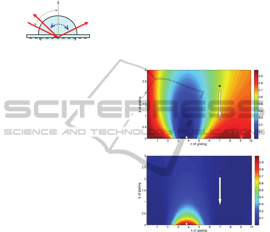
the optimal grating structure is assumed to be of a
period of 600 nm and a duty-ratio of 50%.
Figure 1: Schematic of the proposed optical switch by
PCM grating. Light is coupled in and out by the top semi-
cylindrical prism. The incidence angle of input light is
indicated by
.
To show how the diffraction efficiency of the
grating depends on the refractive index, Figure 2
shows the simulated efficiencies of specular
reflection and first diffraction order as the contour
maps with regard to the grating’s refractive index n
+ i k. The simulation was carried out by the rigorous
coupled wave analysis (RCWA) method (Moharam
and Gaylord, 1982); (Li, 1997) for the optimal
grating with an incidence angle of 62° and an s-
polarization input. In the maps, the refractive indices
of a popular phase change material, Ge
2
Sb
2
Te
5
(GST), are represented by the white and black dots
for its two phase states. GST material was invented
by Yamada et al. (1987) and is an important PCM
because of its superior crystallization speed and
large refractive index contrast during phase change.
For the optical switch applications, this material is
also a good candidate because its amorphous state is
virtually transparent at 1.55 m wavelength (n + i k
= 3.8 + i0.05, as measured by our spectroscopic
ellipsometer), and its crystalline state has a moderate
absorption (n + i k = 7.0 + i 2.3).
According to Fig. 2, we can see that, when the
grating is in amorphous state (white dots), the
specular reflection efficiency is almost zero, while
the first diffraction has a very high efficiency of
92%. On the other hand, when the grating turns into
crystalline state (black dots), the efficiency of
specular reflection is about 60% but that of first
diffraction becomes negligible. All other orders of
diffraction are computed to be zero. Therefore, by
properly controlling the phase state of a grating
made of GST, we can turn on/off the specular
reflection light, or steer the inputted light to either
the specular reflection direction or the first
diffraction direction. Thus it can be used as an
optical path router. The first diffracted beam can
even be designed to couple back to the input
direction and diverted to other route by a circulator,
thus simplifying the optical coupling at input port.
The relatively poor reflection efficiency for the
crystalline state grating (black dot in Fig. 2(a)) is
due to the relatively larger absorption of crystalline
GST. As indicated by the arrows, if a PCM with
lower k becomes possible, a higher reflection
efficiency and lower first diffraction are achievable
for the crystalline state. In fact, Strand et al. (2006)
has tried and succeeded in tuning the absorption of
GST to a much lower value by adding some alloy
composition.
(a) Specular reflection
(b) First diffraction order
Figure 2: Contour maps showing the diffraction
efficiencies of specular reflection and first diffraction
order as functions of the refractive indices of PCM
grating. The white dots indicate the n + i k of the
amorphous GST material, and the black dots indicate that
of the crystalline GST. A lower absorption k for the
crystalline GST is desirable for better crystalline
performance. The incidence angle
is assumed to be 62°.
It should be noted that the above behaviour does
not apply to a p-polarization light because of the
inherent anisotropy in the grating structure. The p-
polarized light always comes out as specular
reflection. From another point of view, the PCM
grating may also be used as a switchable
polarization splitter where the s-polarization can be
Specular
reflection
Prism
Quartz
substrate
PCM grating
Input light
1
st
diffraction
PHOTOPTICS2013-InternationalConferenceonPhotonics,OpticsandLaserTechnology
102
selectively separated from the specular reflection
port.
3 FABRICATION OF THE PHASE
CHANGE MATERIAL
GRATING
According to numerical simulations, the optimized
grating structure is a GST grating of 50 nm thickness
and a 300 nm line-and-space. We had used electron-
beam (EB) lithography to fabricate this sub-
micrometer PCM grating on a silica substrate. For
easy optical alignment, a large grating area of 22
mm
2
is preferable. It turned out that this large area of
electron beam writing is quite challenging because
of the charging-up effect on a silica substrate. We
had to choose a lower electron acceleration voltage
and carefully coat the resist film with a conducting
polymer layer (Epacer 300). After hours’ EB writing
a rather uniform grating structure was obtained.
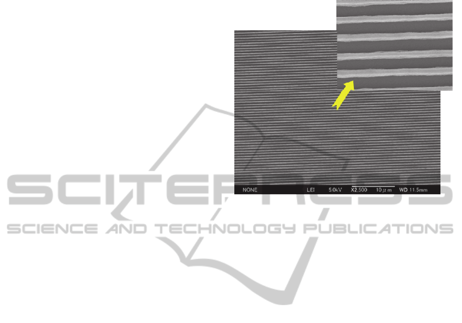
To make the fabrication process simpler and
cheaper, later we shifted our process to the laser
interference lithography where a Lloyd’s mirror
interferometer (Fucetola et al., 2009) was built up. A
He-Cd laser of 441.6 nm wavelength was used as the
optical source. The sample holder was located at
about 70 cm far away from the spatial filter, and the
holder angle α is set as 68.4° in order for the grating
period to be 600 nm (as period = /2cosα). The
diluted photo-resist OFPR800 was found to be
sufficiently sensitive at the wavelength of 441.6 nm
and have adequate resolution to produce the 300 nm
line and space pattern. By carefully tuning the
exposure time and develop time to the optimal
condition, a large area (13 cm
2
elliptic shape) of
uniform grating could be developed in very short
time. An example of such made grating pattern is
shown in Fig. 3. Because of the existence of small
residual fluctuation in wavefront of our interference
system, the grating lines also show some
fluctuations when observed under a scanning
electron microscope (SEM), and are less uniform
than those fabricated by EB lithography.
Nevertheless, it is expected that the fluctuation will
not affect much when conducting the optical
experiment.
Then, a GST PCM layer was deposited on the
resist pattern with a reactive RF-magnetron
sputtering system (CFS-4ES by Shibaura Co.) in an
Ar gas atmosphere. The pressure of the Ar gas was
set to 0.5 Pa and the RF power was set to 100 W to
keep the sample cool enough. After lifting-off in
acetone, a GST grating of designed period was
obtained.
Figure 3: SEM image of the grating pattern fabricated by
laser interference lithography.
4 STATIC DIFFRACTION
MEASUREMENTS
To validate the switching behaviour given by
Section 2, we measured the static optical diffraction
of the GST grating when it is in the amorphous or
crystalline state. All the measurements were
performed on a modified spectroscopic ellipsometer
(VASE by J. A. Woollam Co., Inc). We used the
ellipsometer simply as an optical platform, to take
advantages of its convenient optical coupling system
as well as the precise goniometric mechanism. The
equipment’s standard sample holder and stage were
replaced by a handmade stage together with other
optical gadgets in order to implement the
Kretschmann configuration. In addition, the
hardware control setting has been customized to
allow the angles of input and output arms to be set
independently. In this way, for a fixed incident
beam, we can measure its diffraction at any
direction.
In Figure 4(a), the specular reflection efficiency
of s-polarized light for an amorphous GST grating
was measured for different incident angle
. The
reflection of the no-grating area was also measured
and plotted in the same figure as a reference. Indeed
as the incidence angle
goes beyond the total
reflection angle, the specular reflection drops
quickly because of the diffraction by the grating.
This behaviour agrees well with the light scattering
ImplementationofaGrating-typeSpatialOpticalSwitchbasedonPhaseChangeMaterialanditsStaticMeasurement
103
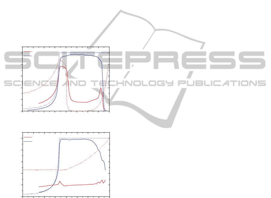
predicted by simulation which is also plotted in the
same figure with dotted line. However, the residual
specular reflection at incidence angles larger than
55° does not go to zero. The reason is considered to
be due to imperfection of the PCM grating.
Next, to conduct the measurement for a
crystalline GST grating, the as-deposited amorphous
GST grating sample was annealed at 200°C for 5
minutes to convert into the crystalline state. The
measured results are shown in Fig. 4(b). As
expected, the specular reflection does not show a
fast drop. However, the overall amplitude is quite
lower than simulation which might also be due to
fabrication error and large absorption in crystalline
GST. Especially the thickness of GST was suspected
to be thicker than designed.
10 20 30 40 50 60 70 80 90
0.0
0.2
0.4
0.6
0.8
1.0
Specular reflectivity [a.u.]
Incidence angle [
o
]
grating area
no grating area
(a) Amorphous GST grating
10 20 30 40 50 60 70 80 90
0.0
0.2
0.4
0.6
0.8
1.0
Specular reflectivity [a.u.]
Incidence angle [
o
]
grating area
no grating area
(b) Crystalline GST grating
Figure 4: Measured specular reflection efficiency of
s-polarized light for a GST grating. The optical
wavelength is set as 1.55 μm. The specular reflection of
no-grating area is also measured as a reference. In
addition, the simulation results are plotted in dotted lines.
5 CONCLUSIONS
To verify the concept of a spatial grating-type PCM
optical switch, we have fabricated the designed
grating structure using electron-beam lithography
and laser interference lithography techniques. The
laser interference lithography is especially useful to
generate large area periodical pattern. The static
switching characteristic of the grating was verified
by optical diffraction measurements for both the
amorphous and crystalline states, and they agree
roughly with the theoretical expectations. We
believe that further precise control in fabrication will
improve the experimental results. In the future,
dynamic phase change by laser pulse will be
necessary to testify the switching actions. The
optical switch can be driven by a more absorptive
visible wavelength to switch between its two phase
states, just as what have been done in an optical disk
system. In addition, PCM with a lower absorption at
1.55 m is greatly desirable in order to improve the
switching efficiency of the crystalline state switch.
ACKNOWLEDGEMENTS
This study was supported by a grant from the
Industrial Technology Research Program, 2011, of
the New Energy and Industrial Technology
Development Organization (NEDO), Japan. A part
of the fabrication work was conducted at AIST
Nano-Processing Facility, supported by
“Nanotechnology Network Japan” of the Ministry of
Education, Culture, Sports, Science and Technology
(MEXT), Japan.
REFERENCES
Burr, G. W. et al., 2010. Phase change memory
technology. Journal of Vacuum Science & Technology
B: Microelectronics and Nanometer Structures, 28(2),
pp.223–262. doi:10.1116/1.3301579.
Fucetola, C. P., Korre, H. & Berggren, K.K., 2009. Low-
cost interference lithography. Journal of Vacuum
Science & Technology B: Microelectronics and
Nanometer Structures, 27(6), p.2958. doi:10.1116/
1.3245990.
Ikuma, Y., Saiki, T. & Tsuda, H., 2008. Proposal of a
small self-holding 2×2 optical switch using phase-
change material. IEICE Electronics Express, 5(12),
pp.442–445. doi:10.1587/elex.5.442.
Ikuma, Y. et al., 2010. Small-sized optical gate switch
using Ge
2
Sb
2
Te
5
phase-change material integrated
with silicon waveguide. Electronics Letters, 46(5),
pp.368–369. doi:10.1049/el.2010.3588.
Li, L., 1997. New formulation of the Fourier modal
method for crossed surface-relief gratings. Journal of
the Optical Society of America A, 14(10), pp.2758–
2767. doi:10.1364/JOSAA.14.002758.
Moharam, M. G. & Gaylord, T. K., 1981. Rigorous
coupled-wave analysis of planar-grating diffraction.
PHOTOPTICS2013-InternationalConferenceonPhotonics,OpticsandLaserTechnology
104

Journal of the Optical Society of America, 71(7),
pp.811–818. doi:10.1364/JOSA.71.000811.
Ovshinsky, S. R., 1968. Reversible Electrical Switching
Phenomena in Disordered Structures. Physical Review
Letters, 21 (20), pp. 1450–1453. doi: 10.1103/
PhysRevLett.21.1450.
Raoux, S., Wojciech Wełnic & Ielmini, D., 2010. Phase
Change Materials and Their Application to
Nonvolatile Memories. Chemical Reviews, 110(1),
pp.240–267. doi:10.1021/cr900040x.
Strand, D. et al., 2006. Optical routers based on ovonic
phase change materials. In Proceedings of European
Phase Change and Ovonic Symposium (Grenoble,
France, 2006). http://www.epcos.org/library/
Library2006.htm.
Wang, X. et al., 2009. Proposal of a grating-based optical
reflection switch using phase changematerials. Optics
Express, 17 (19), pp. 16947–16956. doi: 10.1364/
OE.17.016947.
Yamada, N. et al., 1987. High Speed Overwritable Phase
Change Optical Disk Material. Japanese Journal of
Applied Physics, 26S4(Supplement 26-4), pp.61–66.
doi:10.1143/JJAPS.26S4.61.
ImplementationofaGrating-typeSpatialOpticalSwitchbasedonPhaseChangeMaterialanditsStaticMeasurement
105
