
DATA ACQUISITION ELECTRONICS FOR PET
MAMMOGRAPHY IMAGING
Carlos Leong
1,2
, Pedro Machado
1,2
, Vasco Bexiga
1,2
, J. Paulo Teixeira
1,2
, Isabel C. Teixeira
1,2
1
INESC-ID, Lisboa, Portugal
2
Instituto Superior Técnico, UTL, Lisboa, Portugal
Joel Rego
3
, Pedro Neves
3
, Fernando Piedade
3
, Pedro Lousã
3
Pedro Rodrigues
4
, Andreia Trindade
4
, R. Bugalho
4
, J. F. Pinheiro
4
, M. Ferreira
4
, João Varela
2,4
3
INOV, Lisboa, Portugal
4
LIP-Lisboa, Lisboa, Portugal
Keywords: PET mammography, Breast cancer, Data communication, Synchronism, Multi-clock domains.
Abstract: The purpose of this paper is to present recent developments in the off-detector electronics of a PET
(Positron Emission Tomography) system for mammography imaging. In particular, problems and solutions
associated with the integration of its Data Acquisition Electronics are targeted. Synchronism is a critical
issue in the DAE system. A resynchronization module is proposed to solve communication problems with
the internal asynchronous busses with limited degradation of the communication rate, as compared with
fully synchronous solutions. Data processing refers to 64 dual-channels, 11bit/channel, at a frequency of
100MHz. The maximum of the DAE output rate is 220 MB/s corresponding to 1 MCoincidence/s. The
robustness of the proposed solutions has been validated with software simulation and hardware
implementation. Results of test and validation on FPGA, boards and buses are presented.
1 INTRODUCTION
PET (Positron Emission Tomography) systems are
among the most effective imaging-based
technologies for medical diagnosis. In this
contribution, the final development of a PET system
for mammography - PEM (Positron Emission
Mammography) dedicated to the analysis of the
women breast (Santos, 2004) is described. Emphasis
is given to the integration aspects of the Data
Acquisition Electronic (DAE), which is responsible
for the off-detector acquisition and processing of the
PEM system.
Main aspects of the development of the entire
system, namely, the high level architecture, the
study of the crystal detectors (Lecoq, 2002) (Abreu,
2006), the transducers to sense the light and to
transform it into energy pulses, the associated Front-
end Electronics (Albuquerque, 2006), the off-
detector electronics (Bento, 2006) (Leong, 2006),
(Varela, 2005), the imaging reconstruction
procedures and, of course, the mechanical aspects of
the robot have been reported earlier. In the
identification of system requirements, software
models have been used and extensive Monte Carlo
simulations (Agostinelli, 2003) (Rodrigues, 2004)
(Trindade, 2004) have been performed.
This paper focuses on the difficulties associated
with system integration, and how those difficulties
have been overcome.
Main problems have been found in implementing
adequate communication infrastructures, satisfying
synchronism and performance requirements. In fact,
correct individual sub-systems functionality and
performance was verified in stand-alone test.
Nevertheless, several modifications were required
when integration took place, specifically on sub-
systems that communicate with different clock
domains. A typical case regards subsystems that
access the buses. The purpose of this paper is to
present innovative solutions which have been
designed and implemented to solve those problems.
192
Leong C., Machado P., Bexiga V., Paulo Teixeira J., C. Teixeira I., Rego J., Neves P., Piedade F., Lousã P., Rodrigues P., Trindade A., Bugalho R., F.
Pinheiro J., Ferreira M. and Varela J. (2009).
DATA ACQUISITION ELECTRONICS FOR PET MAMMOGRAPHY IMAGING.
In Proceedings of the International Conference on Biomedical Electronics and Devices, pages 192-197
DOI: 10.5220/0001533001920197
Copyright
c
SciTePress
The paper is organized as follows. In section 2,
the generic architecture of the PEM system is
provided to highlight the communication
infrastructure. In section 3, the DAE functionality
and architecture are described, highlighting the
critical sub-modules, in terms of the communication
environment. Section 3 also contains the proposal of
new architectures for modified modules that are
responsible for the communication between the
DAE and the Front End electronics and between the
DAE and the imaging reconstruction computer. In
section 4, details of the physical implementation are
provided. Section 0 presents the hardware validation
results. Finally, in section 6, the main conclusions
and future work are outlined.
2 PEM SYSTEM
The main objective of the system is to identify the
presence of cancer cells in women breasts. Imaging
reconstruction is used for the purpose. As it is well
known, image reconstruction quests for large
amounts of data. Therefore, main characteristics of
PEM system are high data volumes and high data
rates.
A key aspect is the need to guarantee that
meaningful data is unequivocally identified. In order
to understand what we refer as meaningful data, it is
necessary to understand PEM underlying physics.
Human cells emit γ rays when a radioactive
substance is injected into the human blood stream.
When this occurs, 2 γ ray photons are emitted in
opposite directions over a linear trajectory. Emission
sources are detected by the intersection of
trajectories. 2 ‘planes’ of scintillant crystals detect
the emitted γ ray photons. Crystals emit light that is
afterwards converted into electric signals by
Avalanche Photo Diodes (APD). Crystal arrays in
the PEM scanner are organized in modules and sub-
modules in a hierarchical structure (Amaral, 2007)
(Matela, 2004). Data are captured through 12288
readout channels, organized in 296 identical detector
modules and distributed by the two crystal planes.
Potential meaningful data correspond to the
simultaneous detection of γ ray photons in both
crystal plans. In this case, we consider that a
coincidence has occurred. The underlying principle
of PEM systems behavior is the identification of
coincidences. PEM scanner is a high-resolution
system, capable of detecting breast tumors with
diameters down to 2 mm (Albuquerque, 2006).
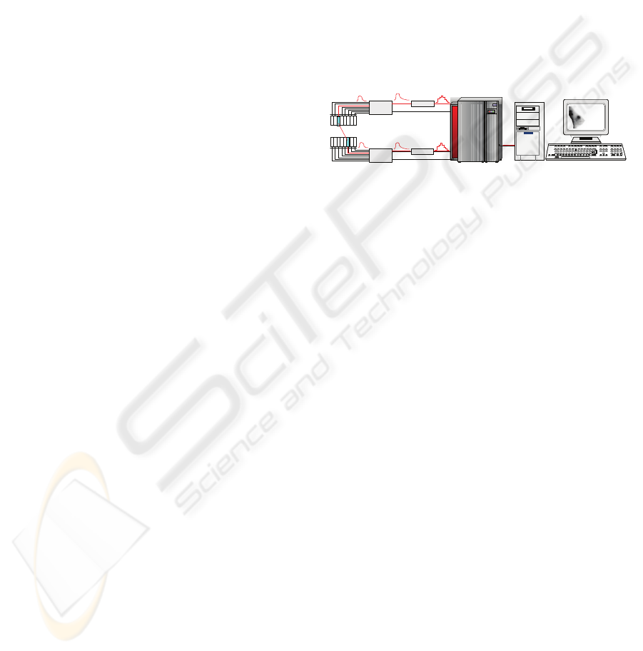
In Figure 1, the top-level architecture of the
Clear-PEM system is depicted. Three main sub-
systems can be identified, namely, the scanner,
constituted by crystals and associated Front-End,
FE, electronics, the off-detector Data Acquisition
Electronics, DAE, and finally, an external computer,
PC (or array of computers) performing data storage
and image reconstruction.
The FE electronics is an analogue/mixed signal
system, responsible for first conditioning of the
signal generated by the APDs, for the
analogue/digital conversion and for the
communication with the off-detector DAE system.
DAE is responsible for digital data processing, in
order to identify coincidences and to send
meaningful data to the computer where image
reconstruction takes place.
Front End
Front End
D
A
E
ADC
PEM
ADC
Control
Contro l
0011010
Figure 1: Top-level architecture of PEM system.
Data integrity must be kept during processing
and communication phases. Otherwise, the diagnosis
result would be unreliable, leading to false positive
or false negative results. This justifies the critical
relevance of the problems tackled in this
contribution.
3 DAE SYSTEM
3.1 DAE Requirements and
Functionality
The main functionality of the DAE is the
identification of relevant data and the transmission
of that data to the image reconstruction computer.
DAE specific requirements are as follows. The
system should support a data acquisition rate of 1
million events per second, under a total single
photon background rate of 10 MHz (Albuquerque,
2006). An event or hit (photoelectric event or
Compton - according to the associated energy) is
defined as the interaction of a γ ray with a crystal.
Data to be analyzed and processed correspond to
the hitting energy in the different crystals, as a
consequence of these interactions. Relevant data is
associated with relevant events (coincidences).
Hence, a relevant event is characterized by the
simultaneous occurrence of hits in both crystal
planes.
DATA ACQUISITION ELECTRONICS FOR PET MAMMOGRAPHY IMAGING
193
3.2 Communication Challenges
Data is transmitted from the FE to the DAE by a
large number of connecting cables, which introduce
various delays, noise, and possibly, signal
degradation. Therefore, physical interconnections
pose a challenge to system integration.
Another challenge is to guarantee the correctness
of data communication between DAE and the data
storage and image reconstruction computer, PC.
A third challenge is to guarantee error-free
communication among DAE boards and chips
through the DAE internal buses, while not degrading
system performance. In the DAE, the minimum
required transmission rate is 1MCoincidence/s at
100 MHz, which corresponds to 220MB/s bit rate.
3.3 DAE Architecture
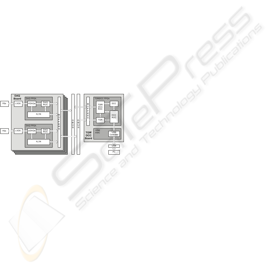
A comprehensive description of the DAE system
(Figure 2) has been published elsewhere. However,
for the sake of clarity, a brief description of the
constituting elements is provided here.
Figure 2: Top-level architecture of the DAE electronic
system.
DAE maps the organization of crystals in the
scanner. As a consequence, DAE is constituted by 4
DAQ (Data Acquisition) boards and 1 TGR/DCC
(Trigger/Data Concentrator) Board, communicating
among them through buses.
The DAQ boards carry out the first data filtering
to identify probably useful data, out of all the data
that floods from the FE. As mentioned, the criterion
for this classification is the detection of coincidence,
interactions of photons with crystal pairs within a
given discrete time interval, to which an identifying
Time Tag is associated. Data is classified either as
(1) useful and stored, or as (2) noise, in which case it
is discarded.
Due to its flexibility, from the technological
point of view, main functionality is implemented
using reconfigurable devices, namely FPGA
technology. Each DAQ board houses two 4-million
gates DAQ FPGA, each containing a read out
controller - the DAQ ROC module. At present, the
DAE houses 4 DAQ and one TRG/DDC boards.
The TGR/DCC board is responsible for the
identification of coincidences. When a coincidence
is detected, TGR/DCC generates a trigger signal that
notifies the DAQ boards of the situation, picks up
the corresponding data and concentrates it according
to a given protocol, to be sent to the external PC for
image reconstruction. The DAE/PC communication
is based on a commercial Bus.
The 4 DAQ and the Trigger boards communicate
through buses, namely, the GBUS (Generic Bus) and
the DBUS (Dedicated Bus) (Figure 2).
3.4 Synchronism between FE and DAE
To guarantee that a detected coincidence is
effectively a coincidence, it is mandatory to know,
without ambiguity, at what time a given data have
been generated. For this, it is mandatory to
guarantee system synchronism. The PEM system is
a GALS (Globally Asynchronous, Locally
Synchronous) system, although FE and DAE are
driven by a system clock.
Data that leaves the FE, at the same time, refer to
the same temporal mark, that is, the same Time Tag.
Moreover, all clock signals driving the system
behavior should have the same frequency and phase.
However, channel links introduce delays. In
order to deal with this situation, data is transmitted
from the FE with the corresponding clocks.
Although, identical cables and components have
been used in identical paths, there is no guarantee
that the clock phase is identical for all local
components where clock is restored. In fact, small
physical differences in the cables, in local PLL,
delays induced by variable thermal maps, clock jitter
and clock skew may result in small phase
differences in the clocks arriving through the
different cables. If these clock signals are very close
to the internal clock edge, it may occur that one is
activated in a given clock cycle and the other be
activated in the following clock cycle.
To solve the FE/DAE synchronization problem,
DAE uses a specific signal, Sync, to guarantee data
synchronism and an auxiliary synchronization
module to guarantee that the synchronism is
restored. Sync behaves as a feedback loop that
makes possible to detect and to synchronize all the
active inputs. The description of this sub-system is
outside the scope of this paper, as it has been
published elsewhere.
BIODEVICES 2009 - International Conference on Biomedical Electronics and Devices
194
3.5 Internal Buses Communication
As mentioned, another challenge in the integration
phase has been the need to guarantee robust
communication among DAE sub-systems. In fact,
each sub-system (e.g., an FPGA) is a clock domain
with its own local clock. Many solutions may found
in the literature, regarding GALS (Xin, 2005),
(Beigne, 2006), (Ogras, 2007).
In our system, data rate transmission is, at least,
220 MB/s. An adequate solution for dealing with
high data rates would be to use a synchronous bus
(Lee, 2007). However, to guarantee robustness on
data transfer, the asynchronous solution is
preferable. Therefore, a trade-off between speed and
robustness is required.
In PEM system, a slightly lower data rate
transfer is acceptable in order to achieve the required
robustness. This means that a small performance lost
(when compared with standard synchronous
solutions) in conjunction with a small increase on
silicon area is acceptable.
Therefore, in the PEM system, subsystems
communicate through asynchronous busses, which
guarantee correct communication at the highest data
rate among these multi-clock domains.
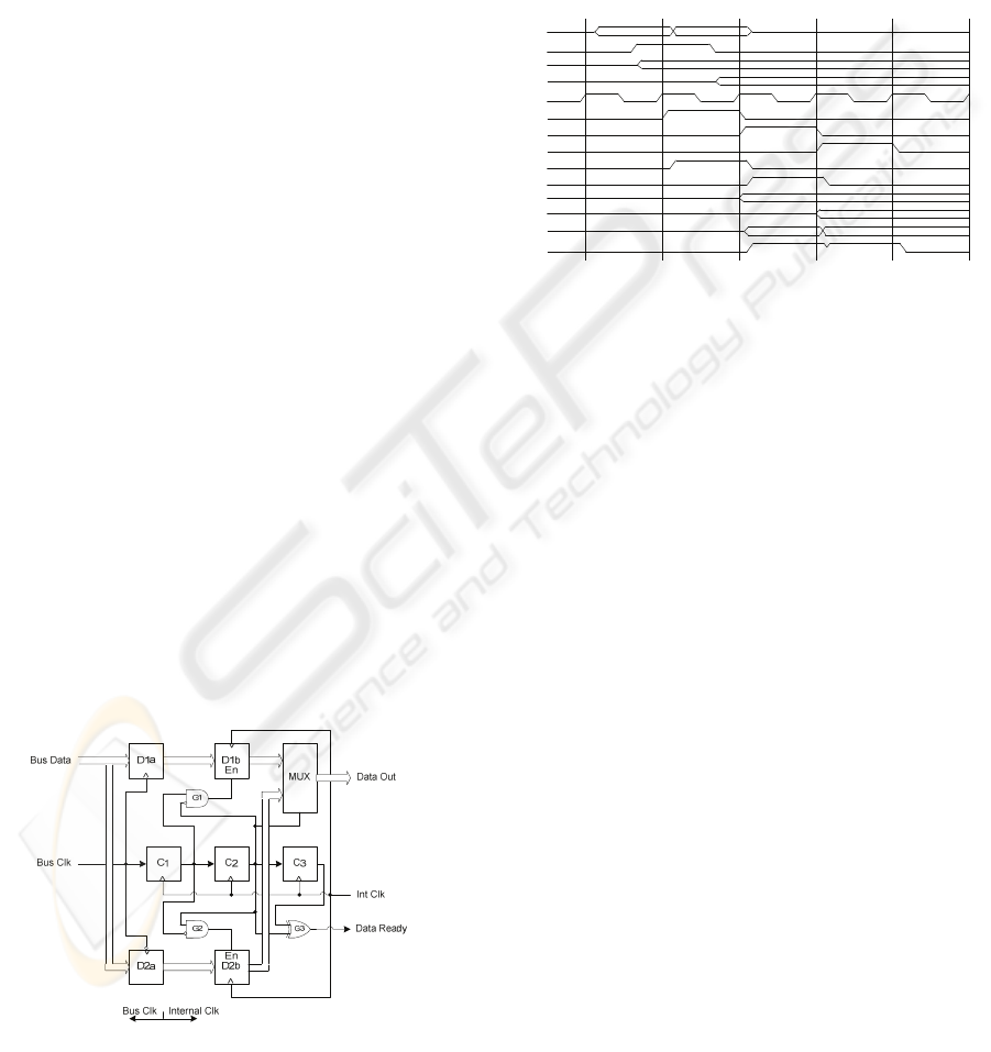
3.6 Resynchronization Module
In the DAE, DBus (Dedicated Bus) and GBus
(Generic Bus), Figure 2, are asynchronous buses. In
this case, Figure 3, two pipeline stages (to guarantee
data synchronization), constituted by 2 chains of 2
Flip-flops each; namely, D1aÆD1b and D2aÆD2b.
Additional flip-flops are used at the input of each
clock domain in order to assess if arriving data is
reliable. In this case, an event is generated and data
communication is started.
Figure 3: Bus Resynchronization block.
The Bus resynchronization timing diagrams
(Figure 4), show that the communication rate is not
as significantly decreased as it would be in a fully
asynchronous solution. This comes from the fact that
each data carries, with it, the corresponding
‘clock’/strobe, avoiding the need to wait for hand
shake protocol as associated with asynchronous
communication.
Moreover, clock domains can work in parallel
with the communication procedure, since they are
locally synchronous domains. By doing so, the speed
of synchronous communication is almost reached.
Bus Data A B
Bus Clk
D1a A
D2a B
Int Clk
C1
C2
C3
G1 (En1)
G2 (En2)
D2a A
D2b B
Data Out AB
Data Ready
Figure 4: Bus Resynchronization timing diagram.
As would in an asynchronous solution,
communication is correctly performed regardless the
bus physical length (limited by the line drivers’
capability). This is a considerable advantage of our
methodology.
3.7 DAE/PC Interconnection
Three solutions have been analyzed and
experimented for the communication link between
DAE and external PC in order to meet speed and
data rate requirements, namely, the PCI, the USB
and the SLINK Fed Kit (CERN). Finally, a mixed
solution based on the USB and the SLINK protocols
has been adopted.
The USB solution is based on the (Cypress
CY7C68013A) microcontroller. Although, the
bandwidth is limited to 60MB/s (maximum
theoretical data rate in USB 2.0 protocol), the USB
link provides a bidirectional communication, able to
handle command requests and consequent replies
(all of each are limited to 64 bits package).
The SLINK (CERN S-LINK Fed Kit) is a
proprietary unidirectional protocol that,
theoretically, achieves up to 800MB/s at full speed.
The SLINK guarantees raw data transmission from
the DAE to the PC.
This USB+SLINK solution allows simultaneous
communication through both links. Separating data
and command communication channels minimizes
the resources needed on the acquisition PC.
DATA ACQUISITION ELECTRONICS FOR PET MAMMOGRAPHY IMAGING
195
4 DAE IMPLEMENTATION
Transmission between FE and DAE is carried out at
frequency of 300MHz (3.3ns) using 32 cables.
Correction is ±1,7ns (±1/2 cycle).
Some electrical problems have been faced, in the
choice of the interconnecting cables. The ideal
would be to use a twisted pair, individually shielded
cable. However, the cross section and the flexibility
of such a set of cables are incompatible with the
mechanical robot. Therefore, a trade-off between
electrical characteristics with mechanical
requirements was necessary.
Main electrical problems that have been faced
are related with the physical distance between the
FE electronics and the DAE (around 6 meters). Most
relevant electrical problems are skew and DC
balance.
Only Amphenol SpectraStrip cables respond to
the system requirements and therefore have been
used in all tests. Nevertheless, some modifications
have still been carried out in this cable in order to
improve electromagnetic characteristics.
DAQ functionality is implemented with 8
Xilinx™ xc2v4000-4bf957 FPGA (2 FPGA per
DAQ Board), i.e., 4 million equivalent gates and 957
pins FPGA. The TGR/DCC functionality is
implemented with one Xilinx™ xc2v3000-4bg728, 3
million equivalent gates and 728 pins FPGA.
The FE/DAE communication between the FE
and DAE subsystems is carried out through LVDS
(Low Voltage Differential Signaling) channel links.
LVDS channel links de-serializer convert the high
speed, serialized, long distance communication lines
into the standard LVTTL (Low Voltage TTL
(Transistor Transistor Logic)) electrical signals at
the input/output of DAQ board’s logic components.
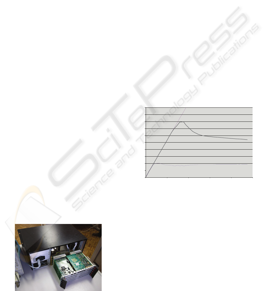
The DAE system is shown in Figure 5. As
mentioned, the DAE is constituted by 5 boards. 4
DAQ boards and 1 TGR/DCC board communicating
among themselves by 2 internal buses (DBus and
GBus).
Figure 5: DAE physical implementation.
Transceivers are used as FPGAs gateways to the
internal BUSes. Transceivers serve also as buffers
for these BUSes.
5 VALIDATION RESULTS
Validation conditions are as follows. Input data
(input events) are provided by a previously
developed system that emulates the Front End (FE)
functionality. Output data has been obtained with the
DAE hardware.
The test strategy is as follows. The electrical test
of the DAE boards has been carried out prior to the
FPGAs functional test. The functionality of the
FPGAs has been validated in silicon (DAE system
and board test).
In Figure 6, the different buses event rate is
represented. It is worth to notice that, these results
have been obtained with a working frequency of
50MHz (limited by current FE hardware version).
This means that if we work at 100MHz, the event
rate duplicates. Therefore, validation results are
beyond system specifications.
0E+00
1E+05
2E+05
3E+05
4E+05
5E+05
6E+05
7E+05
8E+05
9E+05
1E+06
0 500000 1000000 1500000 2000000 2500000
input (FE-EMU) event rate
Dbus rate
Gbus r ate
SLink rate
USB r ate
Event/s
Figure 6: Event rate (experimental result).
The GBus shows a linear dependence of the
event rate on the input rate until almost 700Kevent/s.
After this value, starts to flare until reaching a
maximum transmission rate of 800Kevent/s. After
that, it starts dropping. This is caused by the
inefficiency of the arbiter which is now under
revision. In the linear region, this inefficiency is
masked by the fact that the required bandwidth is
below the maximum.
It is expected that with a more efficient arbiter,
the linearity of the GBus is verified until higher
values and will remain almost constant after that.
SLINK performance in this test is only limited
by the GBus throughput.
BIODEVICES 2009 - International Conference on Biomedical Electronics and Devices
196

6 CONCLUSIONS AND FUTURE
WORK
In this paper, some problems faced during the
integration of the PEM DAE system have been
reported. Emphasis has been put on communication
related problems, particularly, those related with
synchronism aspects.
Some aspects related with the communication
between DAE and FE electronics and the DAE and
the imaging reconstruction computer are provided.
More detail has been given to the solution
proposed for guaranteeing the correctness of the
communication through the DAE internal buses.
With this solution, the robustness of asynchronous
communication and the speed of synchronous
solutions are almost reached.
Experimental results show that the achieved
performance surpassed system specifications.
Additional performance improvements will be
obtained with the review of the GBus arbiter, which
is currently under development.
System architecture is also under review in order
to allow the integration of more data acquisition
boards. This will allow more flexibility in the
scanner geometry, thus allowing extension to the
system applicability for medical imaging of other
regions of the human body. Results will be reported
in the future.
ACKNOWLEDGEMENTS
The work reported in this paper has been partially
supported by FCT (Portuguese Foundation for
Science and Technology), partially supported by
ADI (Portuguese Innovation Agency) in the scope of
the PET II Project 70/00327 and partially supported
by PETSys (Medical PET Imaging Systems, S.A.).
REFERENCES
Abreu, M.C. et al., 2006. Design and Evaluation of the
Clear-PEM Scanner for Positron Emission
Mammography. In IEEE Transactions on Nuclear
Science, vol. 53, Nº. 1, pp. 71-76.
Agostinelli, S. et al., 2003. GEANT4 – A simulation
toolkit, Nuclear Instrum. Meth. A. vol. A 506.
Albuquerque, E. et al., 2006. The Clear-PEM Electronics
System. In IEEE Transactions on Nuclear Science,
vol. 53, nº. 5, pp. 2704-2711.
Bento, P. et al., 2006. “Performance Simulation Studies of
the Clear-PEM DAQ/Trigger System”, IEEE
Transactions on Nuclear Science, vol. 53, nº. 4, pp.
2102-2111.
CERN S-LINK, http://hsi.web.cern.ch/hsi/s-link/
Leong, C. et al., 2006. “Design and Test Issues of an
FPGA Based Data Acquisition System for Medical
Imaging using PEM”, IEEE Transactions on Nuclear
Science, vol. 53, nº. 3, pp. 761-769.
Varela, J. et al., 2005. “FPGA Based Architecture for the
Data Acquisition Electronics of the Clear-PEM
System”, Proc. Int. Workshop on Applied
Reconfigurable Computing (ARC 2005), pp. 131-138.
Rodrigues P. et al., 2004. “Geant4 applications and
developments for medical physics experiments”, IEEE
Trans. On Nuclear Science, vol. 51, pp. 1412-1419.
A. Trindade et al., 2004 .“Design and Evaluation of the
Clear-PEM Detector for Positron Emission
Mammography”, IEEE-Medical Imaging Conference,
Rome.
Santos, A. I. et al, 2004. “Simulation studies and
mechanical system for axillary lymph nodes
examination with Clear-PEM”, Medical Imaging
Conference MIC/IEEE, Rome, Italy.
Amaral, P., et.al. 2007. Performance and quality control of
Clear-PEM detector modules. In Nuclear Instrum.
Meth. Vol. A 580 pp. 1123-1126.
Beigne, E., Vivet, P., 2006. Design of on-chip and off-chip
interfaces for a GALS NoC architecture. In 12th IEEE
International Symposium on Asynchronous Circuits
and Systems.
Lecoq, P., et al., 2002. Clear-PEM, A dedicated PET
camera for mammography, In Nuclear Instrum. Meth.
vol. A 486, pp. 1-6.
Lee, H.G., et. al., 2007. On-Chip Communication
Architecture Exploration: A Quantitative Evaluation
of Point-to-Point, Bus, and Network-on-Chip
Approaches. In ACM Transactions on Design
Automation of Electronic Systems, Vol. 12,No. 3.
Matela, N. et al, 2004. System matrix calculation for
Clear-PEM using ART and linograms. In Medical
Imaging Conference MIC/IEEE.
Ogras, Umit Y., et. al., 2007. Challenges and Promising
Results in NoC Prototyping Using FPGAs. In IEEE
Computer Society.
Santos, A. I. et al, 2004. Simulation studies and
mechanical system for axillary lymph nodes
examination with Clear-PEM, In Medical Imaging
Conference MIC/IEEE.
Xin, Jia, Vemuri, R., 2005. Using GALS architecture to
reduce the impact of long wire delay on FPGA
performance. In Design Automation Conference.
DATA ACQUISITION ELECTRONICS FOR PET MAMMOGRAPHY IMAGING
197
