
Design and Optimization of High-Channel Si
3
N
4
Based AWGs for
Medical Applications
D. Seyringer
1
, A. Maese-Novo
2
, P. Muellner
2
, R. Hainberger
2
, J. Kraft
3
, G. Koppitsch
3
,
G. Meinhardt
3
and M. Sagmeister
3
1
Research Centre for Microtechnology, Vorarlberg University of Applied Sciences,
Hochschulstrasse 1, 6850 Dornbirn, Austria
2
AIT Austrian Institute of Technology GmbH, Donau-City-Strasse 1, 1220 Vienna, Austria
3
ams AG, Tobelbader Strasse 30, 8141 Premstätten, Austria
Keywords: Arrayed Waveguide Gratings, AWG, AWG Design, Silicon Nitride Waveguides, Medicinal Applications,
Photonics, High-Channel AWG, Si
3
N
4
AWG, Optical Spectrometer, High-Index Contrast AWGs.
Abstract: We present the design and optimization of 80-channel, 50-GHz Si
3
N
4
based AWG. The AWG was designed
for TM-polarized light with a central wavelength of 850 nm. The simulations showed that, while the standard
channel count AWGs (up to 40) feature gut optical properties and are relatively easy to design, increasing the
channel counts (> 40 channels) leads to a rapid increase in the AWG size and this, in turn causes the
deterioration of optical performance like higher insertion loss and, in particular, higher channel crosstalk.
Optimizing the design we are able to design 80-channel, 50-GHz AWG with satisfying optical properties.
1 INTRODUCTION
Arrayed Waveguide Gratings (AWGs) are considered
an attractive Dense Wavelength Division
Multiplexing (DWDM) solution because they
represent a compact means of offering higher channel
count technology, have good performance
characteristics, and can be more cost-effective per
channel than other methods (Kaneko, 2002).
However, their performance characteristics depend
largely on the optical properties of the waveguide
materials used. In terms of material, they can all be
divided into two main groups, so-called low-index
and high-index contrast AWGs.
Low-index contrast AWGs (Silica-on-Silicon
(SoS) based waveguide devices) use SiO
2
-buried
rectangular waveguides, usually with a cross-section
of ~ (6x6) µm
2
and a low refractive index contrast
between the core (waveguide) and the cladding of
n
~ 0.75%. They feature many advantages such as low
fiber coupling losses in the order of 0.1 dB and low
propagation loss (Leijtens, 2006). However, the low
refractive index contrast means the bending radius of
the waveguides needs to be very large, which leads to
a rapid increase in the AWG size of several square
centimeters that limits the integration density of SiO
2
-
based photonic devices.
High-index contrast AWGs, such as Silicon-On-
Insulator (SOI) based waveguide devices, use a high
refractive index difference
n ~ 58%. This is
approximately one hundred times higher than that of
typical SoS waveguides. Due to the fact that a
waveguide size decreases proportionally to the
increase in refractive index contrast, the waveguide
size for this material composition shrinks into the
sub-micron scale. Such high-index contrast makes it
possible to guide light in waveguides with a far
smaller bending radius, which leads to a significant
reduction in the AWG size by more than two orders
of magnitude when compared to SoS based AWGs
(Pavesi, 2004). Such compact devices can easily be
implemented on-chip and have already found
applications in WDM systems as well as in emerging
applications such as optical sensors, devices for
biosensing and optical spectrometers for infrared
spectroscopy (Bradshaw, 2005). The main problem
arising from the reduced size of waveguides is the
coupling of light from the fiber into such small
waveguides, which causes much higher coupling
losses, in the order of 10 dB, than in silica AWGs.
The second drawback is the sensitivity of the mode
index to the dimensional fluctuations (e.g. roughness)
of the waveguide, which leads to a rapid increase in
random phase-errors in the fabricated array grating
Seyringer, D., Maese-Novo, A., Muellner, P., Hainberger, R., Kraft, J., Koppitsch, G., Meinhardt, G. and Sagmeister, M.
Design and Optimization of High-Channel Si
3
N
4
based AWGs for Medical Applications.
DOI: 10.5220/0006621002130220
In Proceedings of the 6th International Conference on Photonics, Optics and Laser Technology (PHOTOPTICS 2018), pages 213-220
ISBN: 978-989-758-286-8
Copyright © 2018 by SCITEPRESS – Science and Technology Publications, Lda. All rights reserved
213
arms (Lee, 2000). These technological imperfections
affect the AWG performance by causing a marked
increase in the channel crosstalk. In order to reduce
the roughness of the waveguide sidewalls the high
index contrast AWGs require very high-resolution
fabrication technology that still presents a
considerable challenge today.
An alternative to high-index contrast and low-
index contrast AWGs is the Si
3
N
4
material platform,
which has a moderate index contrast lying between
both main groups (Martens, 2015).
The goal of the silicon nitride waveguide based
AWG development reported in this paper is to take a
significant step towards the integration of spectral
domain optical coherence tomography (SD-OCT)
system operating in a wavelength range of 800 nm to
900 nm and having 0.1 nm resolution. OCT is a
contact-free imaging method, which has become
significantly important in ophthalmology to visualize
the retina. In the course of the project, key-
components of an SD-OCT system will be integrated
on a single optical waveguide chip employing CMOS
compatible processes.
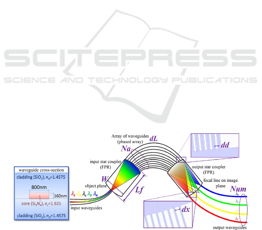
2 AWG PRINCIPLE
Based on the substrate, an AWG consists of an array
of waveguides (also called phased array, PA) and two
star couplers (Fig. 1). One of the input waveguides
launches the light consisting of multiple wavelengths
1
-
n
into the input star coupler, which then
distributes the light amongst an array of waveguides.
The light subsequently propagates through the
waveguides to the output coupler. The length of these
waveguides is chosen such that the optical path length
difference between adjacent waveguides dL equals an
integer multiple of the central wavelength
c
of the
demultiplexer. For this wavelength, the fields in the
individual arrayed waveguides will arrive at the input
of the output coupler with equal phase, and the field
distribution at the output of the input coupler will be
reproduced at the input of the output coupler. In the
output star coupler the light beams interfere
constructively and converge at one single focal point
on the focal line in the image plane. In this way, for
the central wavelength
c
the input field at the object
plane of the input star coupler is transferred to the
center of the image plane of the output star coupler. If
the wavelength is shifted to
c
±
i.e.
1
2
..),
there will be a phase change in the individual PA
waveguides that increases linearly from the lower to
the upper channel. As a result, the phase front at the
input aperture of the output star coupler will be
slightly tilted, causing the beam to be focused on a
different position in the image plane. The positioning
of the output waveguides at the focal points in the
image plane allows the spatial separation of the
different wavelengths (Smit, 1996).
3 AWG DESIGN
AWG design begins with the calculation of its
dimensions, which are essential to create the AWG
layout. The dimensions are given by the geometrical
parameters, as shown in Fig. 1 (Seyringer
1
, 2016):
1. minimum waveguide separation between PA
waveguides (parameter dd),
2. minimum waveguide separation between
input/output waveguides (parameter dx),
3. length of the star coupler (parameter Lf), and
4. optical path length difference between adjacent
waveguides in the phased array (parameter dL).
Figure1: Principle of an AWG with its design parameters and used waveguide cross-section.
PHOTOPTICS 2018 - 6th International Conference on Photonics, Optics and Laser Technology
214

Width of the coupler W is not a dominant
parameter and can be freely changed. In order to
minimize the loss of light capture in the arrayed
waveguides, the number of arrayed waveguides Na
should be sufficiently large. Num is a number of
output waveguides (transmitting channels) that the
AWG is designed for.
There are a couple of commercial photonics tools,
available on the market that can be used to design and
simulate AWGs. Particularly: WDM PHASAR from
Optiwave, APSS Suite from Apollo Photonics, RSoft
tool or Photon Design tool. For our AWG designs, we
used WDM PHASAR, APSS Suite and RSoft tool.
All AWGs were designed for the TM-like mode with
a central wavelength of
c
= 850 nm.
3.1 AWG-Parameters Tool
As the commercial photonic tools do not support (or
only partially support) the calculation of the AWG
geometrical parameters, we developed a new
software tool called “AWG-Parameters” (Seyringer,
2013). This tool significantly reduces the time needed
for AWG design and also facilitates an understanding
of the relationship between input design and
geometrical parameters. The calculations of this tool
are based on the model of Smit and van Dam (Smit,
1996). The tool was used in many low-index contrast
AWG designs and technologically well proven
(Seyringer
1
, 2016). Therefore, we used this tool to
design Si
3
N
4
based AWGs, too.
Figure 2 shows the user interface of this tool,
presenting the design of Si
3
N
4
based 8-channel, 100-
GHz AWG. The input parameters for the calculation
of AWG geometrical parameters are:
Technological parameters used to design waveguide
structure (“Material” window in Fig. 2):
▪ Waveguide structure: width w = 0.8 µm (see also
in Fig. 1 “waveguide cross-section”).
▪ Effective index of the TM-like mode, n
eff,TM
=
1.50912,
▪ n
out
is a refractive index of the cladding (n
cl
) =
1.4575 (in Fig. 1 “waveguide cross-section”).
AWG type parameters (“Transmission Parameters
AWG Parameters” window in Fig. 2):
▪ Number of transmitting channels (output
waveguides): Num = 8 (see also in Fig. 1).
▪ AWG central wavelength (
c
): Lambda (µm) =
0.85.
▪ Channel spacing: df (GHz) = 100.
Transmission parameters (“Transmission Parameters
AWG Parameters” window in Fig. 2):
▪ Adjacent channel crosstalk between output wave-
guides: Cr (dB) = -115.45.
▪ Adjacent channel crosstalk between arrayed
waveguides: CRaW (dB) = -20.7.
▪ Uniformity over all output channels (also called
non-uniformity): Lu
(dB) = 1.
When the “Calculate” button is pressed, the tool
calculates all necessary geometrical parameters given
in Fig. 1 and displays them in the “Transmission
Parameters AWG Parameters” window (Fig. 2):
▪ Number of arrayed waveguides: Na = 51 (see also
in Fig. 1).
▪ Minimum waveguide separation between I/O
waveguides: dx (µm) = 4.000967.
▪ Minimum waveguide separation between PA
waveguides: dd (µm) = 1.200540.
▪ Coupler length: Lf (µm) = 181.927341.
▪ PA waveguide length difference: dL (µm) =
93.185026.
Figure 3 shows the spectral responses of this AWG
simulated with all three photonics tools together with
the measured characteristics of the fabricated AWG
(applying the special taper structures, the fibre
coupling efficiency for the used waveguide structure
is in the range of 1 dB - 1.5 dB).
Minimum Waveguide Separation Between PA
Waveguides (dd): One of the most important AWG
performance parameters is insertion loss. This loss
occurs due to reflection of the light at the facets of
interspaces between the individual PA waveguides.
Light penetrating the cladding material at these facets
is usually absorbed. This loss can be minimized by
maintaining only a small distance between the array
waveguides (parameter dd) or by adding linear tapers;
hence has to be considered already in the AWG
design. Therefore, in the first designs (8-channel,
100-GHz AWGs) we studied the influence of the dd
parameter on AWG performance, mainly on the
losses. We varied this parameter from 1 µm to 1.2
µm, 2 µm and 2.5 µm applying AWG-Parameters
tool. The design parameter dx was kept sufficiently
large, dx = 4 µm (Fig. 2 shows one of these designs).
Parameters dL and Lf were accordingly calculated.
From all simulations was evident that decreasing the
minimum waveguide separation between PA
waveguides led to a strong reduction of the insertion
loss, IL by about 4 dB. In comparison, the linear
tapers, applied in PA waveguides, reduced losses by
less than 1 dB (Seyringer
2
, 2016).
Based on this study and considering waveguide
width, w = 0.8 µm together with the fabrication
limitations we fixed this parameter to dd = 1.2 µm.
Design and Optimization of High-Channel Si
3
N
4
based AWGs for Medical Applications
215
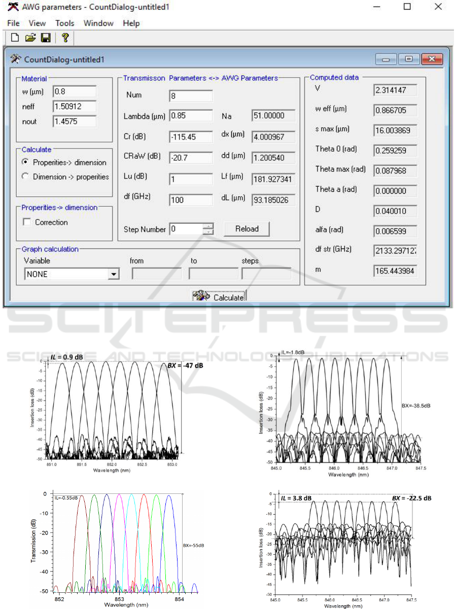
Figure 2: User interface of the AWG-Parameters tool presenting design of 8-channel, 100-GHz AWG.
PHASAR
APSS
RSoft
MEASUREMENT
Figure 3: Simulated spectral responses of 8-channel, 100-GHz AWG from 3 photonics tools together with the measured
characteristics from the fabricated AWG.
PHOTOPTICS 2018 - 6th International Conference on Photonics, Optics and Laser Technology
216

Minimum Waveguide Separation Between
Input/Output Waveguides (dx): In the second step,
it was necessary to fix the design parameter dx, i.e.
minimum waveguide separation between input/
output waveguides. This parameter has an impact on
the crosstalk between adjacent output channels. To
this purpose, four 20-channel, 50-GHz AWGs with
different output waveguide separations were
designed with AWG-Parameters tool: dx = 2.5 µm, 3
µm, 3.5 µm and 4 µm and simulated applying all three
photonics tools (Seyringer, 2017). The simulations
showed that there is some minimum waveguide
separation dx necessary to keep the crosstalk between
output channels sufficiently low (in our AWG design,
dx = 3.5 µm). At this separation, the output
waveguides are positioned far enough from each
other, to prevent the focusing of the power from
selected channel into the neighbour output
waveguides and vice versa. This implies that by
increasing this value the performance of AWG did
not change much (case of dx = 4 µm). If the
waveguide separation was too small, the crosstalk
strongly increased. This is in particular the case of
waveguide separation dx = 2.5 µm and partially dx =
3 µm, where the AWG spectral response contained
side-lobes inducing high channel crosstalk. Based on
this study we fixed this parameter to dx = 3.5 µm.
We would like to point out that all above
described designs were technologically verified and
confirm the simulated results.
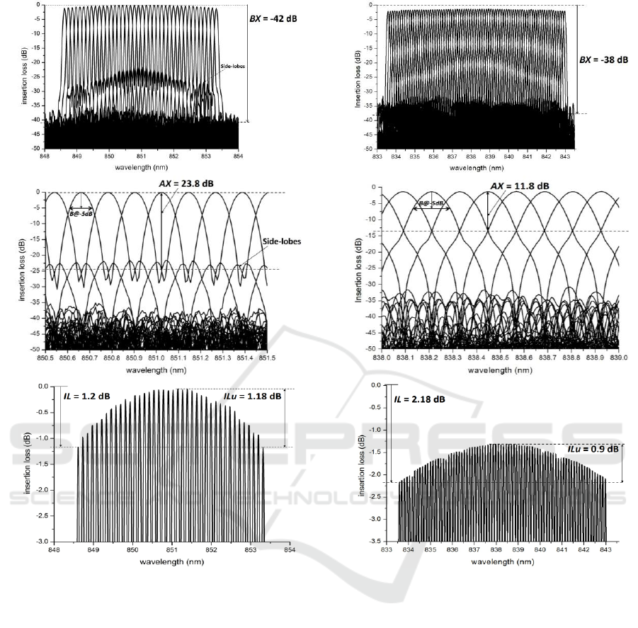
3.2 Design of 40-Channel, 50-GHz
AWG
Based on the previous study we designed 40-channel,
50-GHz AWG. The AWG structure was then
simulated applying WDM PHASAR tool and the
spectral response is shown in Fig. 4. As can be seen,
the transmitted optical signals are well separated from
each other which is confirmed by low background
crosstalk, BX = -42 dB (Fig. 4a). Adjacent channel
crosstalk reached its highest value at the side-lobes in
the middle of the spectrum, AX = 23.8 dB (Fig. 4b).
In addition, the losses are very low (Fig. 4c). There
are nearly no losses in the middle of the
characteristics (the highest peaks) and there is about
1.2 dB loss at the lowest peaks (insertion loss, IL).
This loss is mainly a result of the non-uniformity i.e.
difference between the highest- and the lowest peaks;
also called insertion loss uniformity, ILu = 1.18 dB
(in AWG-Parameters tool labelled as Lu parameter).
From this can be concluded that applying an
optimized design based on the previous study of the
design parameters in order to eliminate losses and
crosstalk, the insertion loss was suppressed nearly to
zero and the channel crosstalk is low, too.
4 DESIGN OF HIGH-CHANNEL
AWGS
Above described optimized design ensures rather
satisfying optical properties of AWGs up to 40
channels. However, the optical spectrometers for
medical applications require much higher AWG
channel counts. We will show that increasing the
number of output channels (parameter Num) brings
some additional design problems to be solved.
4.1 Design of 80-Channel, 50-GHz
AWG
To this purpose, we designed 80-channel, 50-GHz
AWG in which we used the same design parameters,
i.e. dd = 1.2 µm, dx = 3.5 µm; and the parameters Lf
and dL were calculated accordingly (we will call it
DESIGN1). The AWG structure was then simulated
applying WDM PHASAR tool keeping the same
calculation conditions. The simulated spectral
response is shown in Fig. 5. From the characteristics
is evident that the optical signals are much wider
compared to 40-channel, 50-GHz AWG (defined
through the bandwidth, B@5dB, and B@20dB, i.e. a
width of optical signal, measured at a −5 dB, and −20
dB drop from transmission peak), as can be seen in
Figs. 4b and 5b. It causes the increase of insertion loss
by nearly 1 dB (IL = 2.18 dB in Fig. 5c) and
particularly much higher adjacent channel crosstalk,
AX = 11.8 dB (Fig. 5b). Non-uniformity ILu is similar
in both cases, since both AWGs were designed to
have insertion loss uniformity about 1 dB.
Background crosstalk, BX increased from -42 dB (40-
channel AWG) to -38 dB (80-channel AWG, Fig. 5a).
4.2 Optimization of 80-Channel,
50-GHz AWG Design
Since the same design procedure as well as the same
simulation conditions were used in both designs the
question is what is the reason for such widening of the
optical signals causing deterioration of the optical
properties of designed 80-channel, 50-GHz AWG and
how can be this negative effect eliminated.
We have tested various AWG design parameters
and the deep study of the results showed that the
reason for widening of the optical signals is the
crosstalk caused by the coupling between PA
waveguides.
Design and Optimization of High-Channel Si
3
N
4
based AWGs for Medical Applications
217
a)
b)
c)
Figure 4: a) Simulated spectral response of 40-ch, 50-GHz
Si
3
N
4
AWG; b) detailed view of adjacent channel crosstalk,
AX in the middle of the spectrum, c) detailed view of
insertion loss, IL and insertion loss uniformity, ILu.
With increasing the number of output waveguides
(parameter Num) the number of waveguides in the
phased array (parameter Na) also increases and the
optical path length difference between waveguides
decreases. Therefore, the PA waveguides are placed
much closer to each other. From this follows that the
crosstalk caused by coupling in the PA can be avoided
by increasing the separation between arrayed
waveguides (Smit, 1996).
To show this influence we have designed the same
80-channel, 50-GHz AWG but with a different
parameters, dd = 1.75 µm (DESIGN2) and dd = 2.2
µm (DESIGN3) keeping the parameter dx = 3.5 µm.
a)
b)
c)
Figure 5: DESIGN1 - a) Simulated spectral response of 80-
ch, 50-GHz Si
3
N
4
AWG; b) detailed view of adjacent
channel crosstalk, AX in the middle of the spectrum, c)
detailed view of insertion loss, IL and insertion loss
uniformity, ILu.
Figure 6 and Figure 7 show the simulated spectral
responses of both AWG designs.
From the simulations is evident that the shape of
optical signals is similar to the signal shape presented
in Fig. 4 (40-channel, 50-GHz AWG). It ensures
sufficient separation of the signals leading to the
improvement of AWG optical properties.
PHOTOPTICS 2018 - 6th International Conference on Photonics, Optics and Laser Technology
218
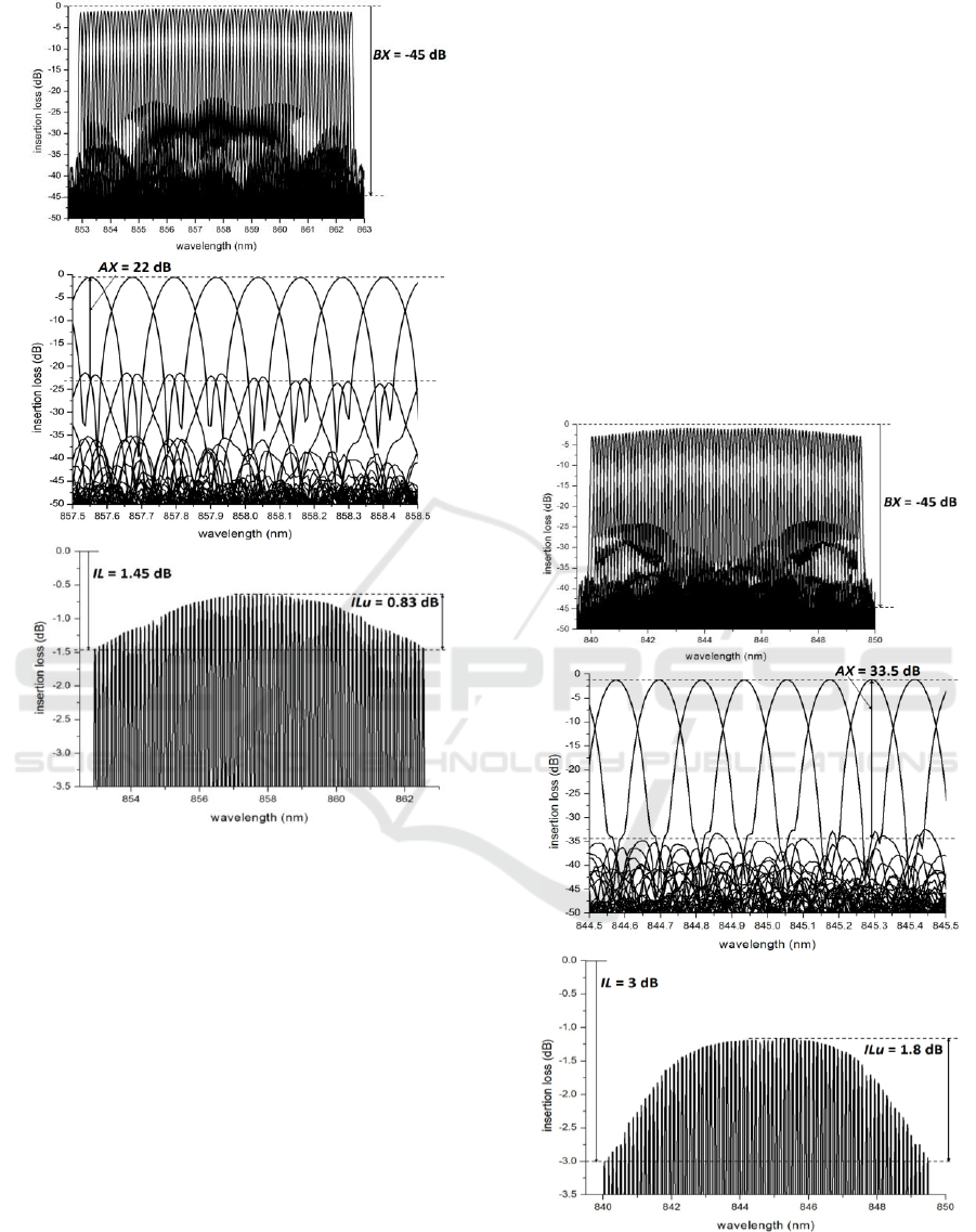
a)
b)
c)
Figure 6: DESIGN2 - a) Simulated spectral response of 80-
ch, 50-GHz Si
3
N
4
AWG; b) detailed view of the adjacent
channel crosstalk, AX in the middle of the spectrum, c)
detailed view of the insertion loss, IL and insertion loss
uniformity, ILu.
5 DISCUSSION
Table 1 summarizes the most important performance
parameters calculated from all four optical responses:
▪ Insertion Loss (IL): As described in section 3,
decreasing the minimum waveguide separation
between PA waveguides (parameter dd) led to a
strong reduction of the insertion loss, IL. This is
in particular the case of 40-channel, 50-GHz
AWG (dd = 1.2 µm) that reached the loss IL = -
1.2 dB. Opposite to this, increasing the distance
between PA waveguides, the losses increased
accordingly, as can be seen in DESIGN2 (dd =
1.75 µm, IL = -1.45 dB) and in DESIGN3 (dd =
2.2 µm, IL = -3 dB). In comparison, the 80-
channel, 50-GHz AWG (DESIGN1), even having
dd = 1.2 µm, features higher losses caused by
widening of the optical signals (IL = -2.18 dB).
▪ Insertion Loss uniformity (ILu): Due to the fact,
that the transmitted wavelengths follow the
envelope described by the far-field of the array
waveguides, there will always be non-uniformity
ILu in the intensity of focal sum-fields (Smit,
1996). Therefore this performance parameter is
also used as an input parameter in AWG design
(see sub-section 3.1), which was set to Lu = 1 dB
(Fig. 2). The non-uniformity calculated from the
simulated spectral responses is similar to this
value in all designs. Here, the small deviations are
the result of the calculation accuracy.
a)
b)
c)
Figure 7: DESIGN3 - a) Simulated spectral response of
optimized 80-ch, 50-GHz Si
3
N
4
AWG, b) detailed view of
the adjacent channel crosstalk, AX in the middle of the
spectrum, c) detailed view of the insertion loss, IL and
insertion loss uniformity, ILu.
Design and Optimization of High-Channel Si
3
N
4
based AWGs for Medical Applications
219
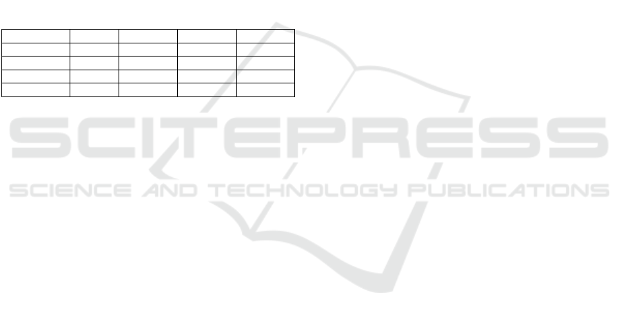
▪ Adjacent Channel Crosstalk (AX): the highest
channel crosstalk between the neighbour output
waveguides (AX = 11.8 dB) was reached in
DESIGN1 with the widest shape of optical
signals. Since the other designs (40-channel, 50-
GHz AWG, DESIGN2 and DESIGN3) feature
similar spectral responses also the calculated
channel crosstalks are similar to each other (AX =
22-23 dB) and they all are much lower compared
to DESIGN1. Lower channel crosstalk means
higher channel isolation.
▪ Background Crosstalk (BX): this parameter
follows the adjacent channel crosstalk parameter,
AX, i.e. the worst value was reached for the
DESIGN1 (BX = -38 dB). All other designs
reached similar values ensuring much higher
background isolation.
Table 1: Performance parameters calculated from all optical
responses.
IL (dB)
ILu (dB)
AX(dB)
BX(dB)
40-ch AWG
-1.2
1.18
23.8
-42
DESIGN1
-2.18
0.9
11.8
-38
DESIGN2
-1.45
0.83
22
-45
DESIGN3
-3
1.8
23
-45
6 CONCLUSIONS
We showed that the design of standard channel count
AWGs (up to 40) is relatively easy and ensures good
AWG performance, too. Increasing the channel
counts (> 40 channels) leads to the deterioration of
optical properties like higher insertion loss and, in
particular, higher channel crosstalk. This appears due
to widening of the optical signals caused by light
coupling between PA waveguides. To avoid this
effect, the minimum separation between arrayed
waveguides has to be increased, i.e. the PA
waveguides have to be placed further apart. However,
it is important to point out that the greater distance
between PA waveguides means the higher losses.
Therefore, the DESIGN2 is the most suitable since
this AWG has optical properties the closest to
optimized 40-channel, 50-GHz AWG.
Finally, based on this study we designed 160-
channel, 50-GHz AWG having the optical properties
very similar to 80-channel, 50-GHz AWG. All high-
channel AWG designs are going to be technologically
verified. Based on the measured data, the next step is
the design of 320-channel, 42-GHz AWG.
ACKNOWLEDGEMENTS
This work was carried out in the framework of the
project COHESION, no. 848588, funded by the
Austrian Research Promotion Agency (FFG).
REFERENCES
Kaneko, A., et al., 2002. Design and applications of silica-
based planar lightwave circuits. J. Sel. Top. Quantum
Electron. 5(5), pages 1227–1236.
Leijtens, X. J. M., et.al., 2006. Wavelength filters in fibre
optics, in Arrayed Waveguide Gratings, 123, pages
125–187.
Pavesi, L., Lockwood, D. J., 2004. Silicon Photonics,
Springer, Berlin.
Bradshaw, J. T., Mendes, S. B. and Saavedra, S. S., 2005.
Planar integrated optical waveguide spectroscopy.
Anal. Chem. 77, pages 28A–36A.
Lee, K., et al., 2000. Effect of size and roughness on light
transmission in a Si/SiO2 waveguide: experiments and
model, Appl. Phys. Lett. 77, pages 1617–1619.
Martens, D., et al., 2015. Compact silicon nitride arrayed
waveguide gratings for very near-infrared wavelengths.
IEEE Photonics Technol. Lett. 27, pages 137–140.
Smit, M. K., et al., 1996. PHASAR-based WDM-devices:
principles, design and applications. J. Sel. Top.
Quantum Electron. 2, pages 236–250.
Seyringer
1
, D, 2016. Arrayed waveguide gratings, in SPIE
Spotlights - New e-book series, SPIE Press, P.O. Box
10, Bellingham, Washington 98227-0010 USA.
Seyringer, D., at al., 2013. AWG-parameters: new software
tool to design arrayed waveguide gratings, in
Proceedings SPIE 8627, 862716.
Seyringer
2
, D., et al., 2016. Design and Simulation of
Si3N4 Based Arrayed Waveguide Gratings Applying
AWG-Parameters Tool. In Proceedings of the 18th
International Conference on Transparent Networks
(ICTON 2016), 978-1-5090-1466-8/16, We.C5.5.,
Trento, Italy.
Seyringer, D., et al., 2017. Design and simulation of 20-
channel, 50-GHz Si3N4 based arrayed waveguide
grating applying AWG-Parameters tool. In
Proceedings of SPIE Photonics West 2017, Integrated
Optics: Devices, Materials, and Technologies XXI,
Paper 101061L, San Francisco.
PHOTOPTICS 2018 - 6th International Conference on Photonics, Optics and Laser Technology
220
