
Nanoscale Non-Contact Laser Measurement of Precision Machine
Tooling and Optical Surfaces
Schubert Soãres
Ultrafast Sensors, 6774 E 123
rd
Ave, Brighton, CO 80602, U.S.A.
Keywords: Non-Contact Nano Metrology, Laser Triangulation, Optical Scatter, Machine Tool Error, Surface
Topography, Edge Structure, Defect Geometry, Thin Films.
Abstract: Optical and semiconductor products are fabricated utilizing industrial technology that is steadily progressing
to nanometre accurate operations. Reliable non-invasive contact-free sensors and techniques are required to
monitor in situ manufacturing parameters in parallel with product formation. The real-time evaluation and
analysis of precision fabrication processes could lead to intelligent, computerized, sensor-actuated
implementation, with automated compensating feedback loops to facilitate nanometre accuracy and
consistently provide high quality products in abundant yield. Laser triangulation is demonstrated herewith
as a versatile solution to simultaneously measure machine tool components and monitor the product in
process. Optically levered reflection resolved on a nanometre resolution displacement sensor, enables the
analysis of spindle axial and rotational error, stage linear error, the impact of these error-motion components
on a diamond tool edge and its progression to wear, while inspecting the compliance of the product to the
desired surface finish and shape. Scanning optical scatterometry is utilized to image and analyse edges,
surfaces, defects, and thin film structure. This sensor technology is highly adaptable, and may be utilized in
scales ranging from small µm-size to large meter-size products manufactured from a variety of materials.
1 INTRODUCTION
A variety of industrial and consumer products such
as laser optics, mirrors, crystals, thin films, fibre
optic devices, camera optics, semiconductor wafers,
precision aircraft and automotive engine
components, and progressive-focus optical lenses
are routinely manufactured to accuracies, ranging
from a few 100’s to a few nanometres. The
manufacture of these products is implemented with
rigid process control, often utilizing separate
systems for metrology, in uncoordinated
independent procedures. There is vital requirement
in these diverse industries for versatile, integrable,
contact-free, non-destructive, optical sensor
technology to accurately monitor in situ all
dynamics of the fabrication process, machine tool
operating parameters, cutting tools, and product
quality. The measurements range from rotational
(spindle) and linear (stage) error motion, cutter
condition vis-à-vis edge quality and evolution during
usage, machined surface quality and shape
conformity, defects, and manufacturing
repeatability. The potential for co-ordinated
concurrent sensor measurements and computer
assisted parametric control of the manufacturing
process could result in consistent nanometre quality
products with significantly improved yield.
Conventional contact-free techniques such as
capacitive and inductive probes rely on relatively
large sampling areas, and may be inadequate in
terms of convenience, calibration, sensitivity, and
cost for a variety of product materials, shapes, and
sizes. These systems were developed originally for
conductive materials; the non-invasive measurement
of optics or doped semiconductors poses additional
challenges. Shape is another restriction with
calibration posing significant hurdles for spherical,
aspheric, or free form surfaces, restricting usage to
planar products. Other techniques such as
ultrasonics, air pressure, and phase analysis involve
greater hardware complexity and lack nanometre-
level resolution. The measurement of the shape of a
diamond cutting tool, or the structure of a thin film,
or a defect for example, is virtually impossible
utilizing any of these technologies. Since all of
these sensor types require extensive electronic
24
Soãres, S.
Nanoscale Non-Contact Laser Measurement of Precision Machine Tooling and Optical Surfaces.
DOI: 10.5220/0006539900240035
In Proceedings of the 6th International Conference on Photonics, Optics and Laser Technology (PHOTOPTICS 2018), pages 24-35
ISBN: 978-989-758-286-8
Copyright © 2018 by SCITEPRESS – Science and Technology Publications, Lda. All rights reserved
processing and amplification, noise and linearity are
major limiting factors to accuracy and resolution.
Laser triangulation sensing offers a simple,
compact, feasible, micro-to-macro scale solution to
track operating parameters in a variety of industrial
environments, to monitor, evaluate, and analyse the
manufacturing process, and also to measure a
multitude of precision products fabricated from a
variety of materials. Optical-lever metrology, in
which laser reflection and scatter are scanned on a
nanometre-resolution solid state sensor, is
investigated in this paper. This technology is
utilized to easily resolve 100-nm tool displacement,
250-nm error motion, cutting tool shape and wear,
machined surface quality and tolerances, defects,
and composite thin films. The versatility of this
technology resides in simple calibration processes,
easy multi-channel expansion into ordinary data
acquisition and computer systems, and turnkey
integration with precision machine tools.
2 OPTICAL METROLOGY
There are several well established techniques for
optical metrology utilizing the energy (wavelength),
the coherence, and the polarization properties of
laser beams, in electromagnetic interaction with
surfaces and media, derived from the physics of
optical reflection, diffraction, or transmission. The
optical signals are monitored with sensors or
cameras, recorded on data acquisition systems, and
analysed and decoded with software to produce
calibrated metrics for evaluation and quality control.
The foremost of these methods is interferometry
wherein a pair of coherent beams, originating from
the same source (via wavefront or amplitude
division, forming reference and probe beams)
interact when combined after sampling to produce
fringe energy redistributions, which are monitored
singly, sequentially, or collectively to decode a
variety of parameters. The signal could be related to
and utilized to measure, for example, displacement,
three-dimensional (3D) shape, spectral content,
optical properties, and the internal structure of
optically transmissive media. The reflection and
transmission properties of polarized light incident on
near-perfect surfaces, interfaces, and film layers
provides additional opportunities for metrology
based on ellipsometry, Brewsters angle, principal
angle, critical angle and total internal reflection
(Azzam, 1999, Heavens, 1955). These techniques in
fact may be utilized, by comparative analysis of
polarization state, amplitude evanescence, and phase
shift, to measure real and complex optical properties
of media, examine sub-surface structure, or detect
anomalous behaviour at interfaces.
Optical triangulation and scatter, operating with
nanopositioning, are additional options available to
directly evaluate position, displacement, and motion,
and to image surface topography, sub-surface
structure, anisotropies, artefacts, defects, and thin
films.
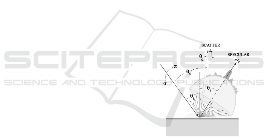
2.1 Laser Reflection and Scatter
Our primary focus is on laser reflection and scatter
from smooth surfaces in optical components,
precision-machined surfaces, Si wafers and similar
products from various high-technology industries.
Any smooth surface with residual nanoroughness
(Figure 1) will produce specular reflection and non-
specular diffractive scatter from an incident optical
beam, which is preferably made diffuse to eliminate
its coherence and minimize speckle. The specular
beam is produced by the flat-smooth surface (zero-
order roughness), and is governed by the vector
Fresnel relations, which are polarization specific.
Figure 1: Geometry of optical scatterometry. Specular
reflection is from the smooth surface. Low to high spatial
frequency microstructure scatters proportionally
decreasing power at wide angles. The omni directional
low-intensity haze is produced by microstructure.
Residual structure in the surface, corresponding
solely to the roughness component of the
topography, can be modelled in a multi-dimensional
Fourier integral (or alternate) analysis, as composed
of sinusoidal (or basis) functions within a continuous
and distributed spread of spatial frequencies (or
components), each with adjustable amplitude and
phase shift, which converges approximately, in the
mean-square, to the surface profile (Church, 1979,
Longuet-Higgins, 1957, Stover, 1995).
Nanoscale Non-Contact Laser Measurement of Precision Machine Tooling and Optical Surfaces
25

The far-field (Fraunhofer) distribution of
scattered optical power from this surface at angle
s
,
from an incident beam inclined at
i
, measured on a
detector subtending solid angle
d
, ranges from its
maximum at the angle of specular reflection
r
,
decreases gradually but not necessarily uniformly or
symmetrically, in ~ 2-steradians oriented (for
detection) in spherical coordinates about the axis of
the reflected beam, centred at the point of reflection
(Figure 1). Since for practicality,
i
is usually not
normal, the spot on the surface is not circular, and
must be accounted for if illuminated structure or
defects are large in comparison. The scatter power
measurement at non-normal angles is compensated
by a factor of (Cos
s
)
-1
to normalize the orientation
of the detector to the plane of the surface. The
altitudinal and azimuthal variation of the scattered
optical power about the specular axis need not
necessarily be regular or asymptotic, and in fact may
contain additional artefacts such as multiple
secondary maxima superimposed with power
fluctuations, uniform haze, and other variations.
The defect size, , and the roughness dimension,
',scaled in comparison to the wavelength,
determine the corresponding total 3D scatter
distribution (Bohren, 1998, Stover, 1995). There are
five zones of scaling, namely:
(І)
(І)
(І)
(І)
and
(І)
These can be restricted
to a few categories for precision surfaces. Scatter
from low spatial-frequency roughness (several
multiples of the optical wavelength; ') is present
in angular proximity to the specular reflection.
Microstructure containing higher spatial frequencies
(') scatters power at wider angles away from the
reflected beam. The scaling determines if the optical
path of scatter radiation is by direct reflection from
the surface or by instances or orders of multiple
reflections within the roughness, prior to impinging
on the detector. The power of the scattered
radiation, if scales with the sixth power of the
dimension of defects, and varies as
-4
. The non-
specular radiation at oblique angles is essentially
Rayleigh scatter produced by randomly oriented
sub-wavelength
(І)
defects, surface, and sub-
surface structure, and studied extensively by Church,
1979, and Stover, 1995. Indeed, scatter produced by
nanostructure, where ' is relatively minor (at multi-
lattice constant or multi-molecular dimensions) in
comparison with , is distributed uniformly over the
entire hemisphere, much as a Lambertian source,
and forms a noise-power baseline. The total power
distribution function may also contain Mie scatter
components from fractional to multi-wavelength
dimension defects (
(І)
), Rayleigh scatter from
sub-wavelength defects (), and a wide range of
features which additionally may be present on the
surface as texture, device patterns, debris, or damage
in a sub-surface region within an optical wavelength.
The remaining critical variables in defect and
artefact detection are the beam incidence angle and
its polarization, the scattering cross section, the spot
profile and size, and the detection arrangement. -
polarized light incident on a defect generates a
symmetric lobular altitudinal pattern oriented
orthogonal to the field, while-polarized light
illuminating a defect produces a uniform altitudinal
scatter distribution but is azimuthally lobular, i.e. a
90-degree rotation of the field. The beam
orientation and the positioning of detectors for
defect detection in the scattering plane is an
empirical art critically based on the selection of the
polarization of the incident beam to enhance high
defect-to-background contrast. For example, the
normal component of –polarization in near normal
incidence could be utilized to probe embedded
defects or voids with narrow oblique detection.
Similarly,-polarization may be useful to detect a
particle on a surface, where oblique incidence is
combined with wide normal detection. Additional
variables to consider are the specific defect shape
(usually not spherical), the defect material, whether
the defect resides on a dielectric or a conducting
surface, and the corresponding image charge
distributions. The operating wavelength may be
judiciously selected if the background surface, the
defect material, and the scatter thus produced are
reasonably well understood. The angular
distribution of scatter also suggests the utilization of
Fourier spatial filtering to distinguish scatter profiles
of a particular roughness range, device footprint, or
defect type, a technique widely in use in the
semiconductor industry to identify undesirable
defects on processed wafers.
Figure 2 shows representative angle-resolved
optical scatter data acquired at 633 nm on a polished
quartz optic, in which the logarithm of the relative
scatter produced is plotted versus the detector
(scatter) angle, which is varied from the incident
beam towards the specular reflected beam. The data
follows our discussion in the previous paragraph,
and the scatter power in relation to the surface
roughness spread is as indicated. The dynamic
range from the specular maximum power (flat
surface) to the scatter minimum power
(nanoroughness) is approximately 73 dB. The
specific scatter power for a defined roughness spread
at a prescribed angle could be resolved by
deliberately machining the corresponding structure
PHOTOPTICS 2018 - 6th International Conference on Photonics, Optics and Laser Technology
26

onto a surface to enable a calibration reference in
this measurement or vice versa. The scatter
produced by an ideal near-perfect smooth flat
reflecting surface would consist of only two
components: the specular beam which would be an
almost mirror image of the incident beam, with an
infinitesimal fraction of the power transferred to
omni directional uniformly distributed Rayleigh-
scatter haze produced at the crystalline level,
establishing the noise threshold. A polished optic, a
precision diamond turned mirror, or a polished Si
wafer are considered ideal surfaces, satisfying
conditions of spatial frequency ergodicity, and
sampling at a single point would produce a perfectly
symmetrical scatter profile, which would be
representative of the entire surface.
Figure 2: The angular optical scatter distribution (at 633
nm / ) measured on polished quartz. The dynamic signal
range is 73 dB. The scatter power is proportional to the
roughness scaled to the wavelength, as indicated.
Another useful figure of merit for comprehensive
surface quality is the normalized total integrated
scatter (TIS), which is produced by the entire
functional structure of the surface and sub-surface,
comprising all roughness and defect-array
constituents with the exclusion of the specular beam
(corresponding to the zero-order smooth surface),
which is filtered from the data. The TIS value may
be utilized to monitor a surface and provide a rapid
measurement of overall quality, during the grinding,
the lapping, and the polishing processes to produce a
smooth flat surface on an optic or a Si wafer. It can
also be utilized to sample defect density per unit area
by common mode comparison of the TIS for a
smooth surface to a surface with distributed defects.
A surface may also be scanned in a TIS system to
provide area-wide metrics for a more exact figure of
merit. An associated figure of merit could be
established by profiling the specular beam for
comparison with the profile of the incident beam to
deduce spatial frequency components of the surface.
Precision industrial environments where optical
components, devices, semiconductor wafers, and
metal parts are manufactured require rapid real time
evaluation and analysis of parameters such as
machine error motion, surface topography, local and
global surface roughness, sub-surface damage,
contamination, shape, thickness, and defects. This
goal is achieved if some of the technical
complications, details, and analysis of scatterometry
(Figure 1), associated with factors such as the angle
of incidence, polarization, beam profile, interaction
with media, coherence, etc., may be circumvented.
A simple in-plane non-invasive linear optical system
consisting of a low power plane polarized laser input
beam with a symmetric profile and a passive,
suitably oriented, uniaxial sensor can be devised to
produce results within constraints of ease of
calibration, expense budget, and low complexity.
Low spatial frequency variations in surface
topography or motion cause well-defined deflections
in the specular reflected beam, and produce
proportional signal fluctuations. If additional
sensors are positioned to measure scatter in
predetermined non-specular angles
s
it is possible to
detect and deduce various surface parameters related
to high spatial frequency content and defects. If the
sensor is capable of resolving minute power
variations, its corresponding sensitivity to surface
features and defects is proportionally enhanced.
2.2 Optical Sensing
Optical sensors with wide dynamic response are
available to track position, and measure
displacement and motion, producing a signal, which
is proportional to the relative distance between two
objects, or range to a moving surface; coordinates
are established by sensor geometry and mounting
configuration, with illumination which can be direct
beam incidence or triangulation. These sensors are
available as single element units or as multi-element
/ dual-dimensional arrays. The sensing element
could be a PIN photodiode, or a CCD or CMOS
sensor, and require external bias and amplification.
Optical sensing circumvents the limitations of
various other non-contact technologies in
measurements of planar and non-planar geometries,
in a smaller footprint, with improved performance,
reliability, and integration.
Nanoscale Non-Contact Laser Measurement of Precision Machine Tooling and Optical Surfaces
27
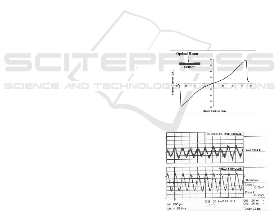
2.2.1 A Displacement Tracking Sensor
A planar multi-dimensional silicon sensor was
demonstrated in which Schottky contact pairs were
deposited and oriented laterally, with the
photosensitive area delimited by the contacts as seen
in the inset in Figure 3. The active area is
illuminated with an optical source, preferably though
not necessarily, in the profile of a collimated or
focused laser beam. The optical radiation is
absorbed in the sensor, inducing excitons, which
instantly diffuse radially away from the point of
injection, electrons dispersing more rapidly than
holes, establishing a steady state charge distribution
centred at the point of injection (Sze, 1981). This
sensor operates on the cascading internal structure of
ambipolar electrical fields, arising from the disparity
in the diffusion distribution geometries of high-
mobility electrons in the conduction band, and low-
mobility holes in the valence band. This field
arrangement modulates the intrinsic fields within the
depletion region at the contacts, and induces a beam
position weighted self bias at each contact, with
unidirectional current flow on average that is
uniquely proportional to the injection point of the
optical beam relative to the contacts (Sze, 1981).
The sensor itself may be presumed to be self
deconvolved and essentially noiseless, since in its
passive mode internal currents, in the absence of
optical input, are symmetrically opposing. If the
beam profile is asymmetrical, or geometrically
irregular with distributed internal power variations,
then this versatile sensor could identify the
weighted-average position of the “maximum” power
of the beam, suggesting applications in sensing
textured or patterned geometries. The sensor signal
is proportional to the position of the beam maximum
within the contacts, as well as to the input optical
power, and also to the relative position between the
plane of the active surface and the source, yielding
resolvable 3D-sensitivity for a variety of
applications in optical systems. The output signal
may be made arbitrarily large to circumvent any
level of input noise available at an amplifier; the
ultimate limitation however being the shot noise in
the optical source, which in effect can also be
minimized by lock-in techniques, feedback control,
and thermal stabilization (Horowitz and Hill, 1989).
2.2.2 Static and Dynamic Sensitivity
This sensor was evaluated for static sensitivity and
dynamic response; representative results are shown
in Figures 3 and 4. In the static mode a 1-mW HeNe
(633 nm) laser source was collimated into a 10X
microscope objective; the beam spot was estimated
at approximately 5 µm. The sensor with 150-µm
active area was fixed to a micropositioning stage.
The stage driver was computer controlled, and the
voltage across the stage was gradually ramped,
sweeping the sensor across the stationary optical
beam from one contact to the opposite contact.
The functional dependence of the signal from the
sensor versus the beam position traversing between
the contacts is measured and processed with low
noise electronics (Figure 3). This signal is shown to
peak in bipolar fashion at the contacts with a null at
the geometric centre. There is piecewise linearity in
the signal, possibly associated with a non-uniform
beam profile, shielding of the optical beam as it
traverses the contact, and non-linear interaction
between the ambipolar field distribution and the
contact fields. Several displacement references are
available for purposes of calibration; the most basic
being that the manufacturer certifies the stage with a
displacement per applied voltage specification. In
addition, the sensor has a lateral active area
dimension, which could also serve as a rigid
reference.
Figure 3: Tracking response of a displacement sensor.
Figure 4: Frequency response of the sensor to a 4.85-kHz
oscillation imposed on the optical beam.
The dynamic response of the sensor was
evaluated utilizing a lock-in technique to explore
low amplitude detectivity and the noise floor. The
PHOTOPTICS 2018 - 6th International Conference on Photonics, Optics and Laser Technology
28
laser was coupled into optical fibre and the fibre was
fixed to a narrow tube piezoceramic with 3 nm/V
displacement calibration. A 50-µm sensor was
attached to a mechanical stage and positioned within
the optical beam in the near field. The spot size was
estimated less than 30 µm full width half maximum.
The lock-in amplifier provided a 4.8-kHz, 80-mV p-
p stimulus to the piezo, and the sensor signal was
simultaneously monitored and measured by lock-in
at 10
5
gain. The stimulus corresponds to a spatial
beam oscillation of approximately 0.25 nm across
the active area of the sensor, and was resolved with
approximately 20% noise (Figure 4). This would
indicate a detection threshold of approximately 0.05
nm, well below the lattice constant of Si. It is
apparent that 1-nm resolution could routinely be
achievable without any constraint.
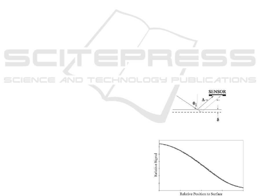
2.3 Metrology by Laser Triangulation
The technology described above is now integrated
and utilized in a computerized system to measure
and evaluate a variety of manufacturing assets,
operating parameters, and precision products. These
range from basic tool position and displacement
sensing, rotary and linear motion sensing, thermal
effects, inertial imbalance, and examination of the
machining operation, to sophisticated inspection of
diamond cutting tools required to fabricate optics,
and imaging of precision machined surfaces, defects,
and thin films. The metrology and imaging system
consists primarily of a stable laser source, a
displacement sensor, a piezo stage with triaxial
scanning capability of 50 µm x 50 µm x 50 µm,
typically with 100-nm pixel resolution, ultra-low
noise electronics, data acquisition, signal processing,
and software analysis. The 785-nm laser is fibre
coupled, and the sensor and the fibre tip are mounted
adjacent, in plane on a base, with adjustments to
enable the applications and measurements detailed
below. The beam spot is typically under 0.1-mm
diameter, and can be adjusted to the application as
necessary. The optical beam and the sensor
arrangement are shown in Figure 5a. This geometry
of optical triangulation is optimal for sensing and
imaging applications, wherein the sensor and the
optical source are mutually aligned at an angle such
that the source beam reflects from the target surface
into the sensor, forming a plane of incidence which
is orthogonal to the surface.
The displacement and motion sensitivity is as
follows: if the plane of the surface moves a parallel
distance away from its reference position (Figure
5a), the optical beam is translated to a new position
on the surface, laterally displacing the reflected
beam across the sensor by a dimension, , producing
a proportional sensor signal. For a triangulation
angle
i
of π/4, the displacement of the beam is
optically levered by a factor of twice the
displacement of the surface; equivalence is
established at ~ π/7. This could be considered a
practical lower limit whereby the formation of a
Wiener wave distribution would not perturb the
sensor, in near-field measurements. The vertical
response (normal to the target surface) of this
configuration over a perpendicular scan of 50 µm is
shown in Figure 5b. The linear response of the
system in the central region is ideal for various
sensing applications, which are explored in the
following sections. The imaging capability of this
system resides in its sensitivity to contrast in scatter
measurements, in a lateral scanning process. Scatter
is measured by positioning a sensor apart from the
specular beam, and adjusting its altitudinal and
azimuthal positions to detect spatial roughness or
defect types, as shown in Figures 1 and 2, and
described in Section 2.1. This system utilizes
software-processing routines to operate scanning
algorithms, interpret signals, and enhance sensor
response to scatter. Evaluations of various
machining parameters and examinations of surfaces,
geometric artefacts (edges), defects, and thin film
layers in 3D measurements are presented in the
following sections, which demonstrate the versatility
of this technology.
Figure 5a: Optical triangulation geometry.
Figure 5b: Response of the sensor-beam arrangement to
displacement, perpendicular to the surface plane.
2.3.1 Torque Offsets and Thermal Analysis
Ultra-precision machine tools are designed as
Nanoscale Non-Contact Laser Measurement of Precision Machine Tooling and Optical Surfaces
29
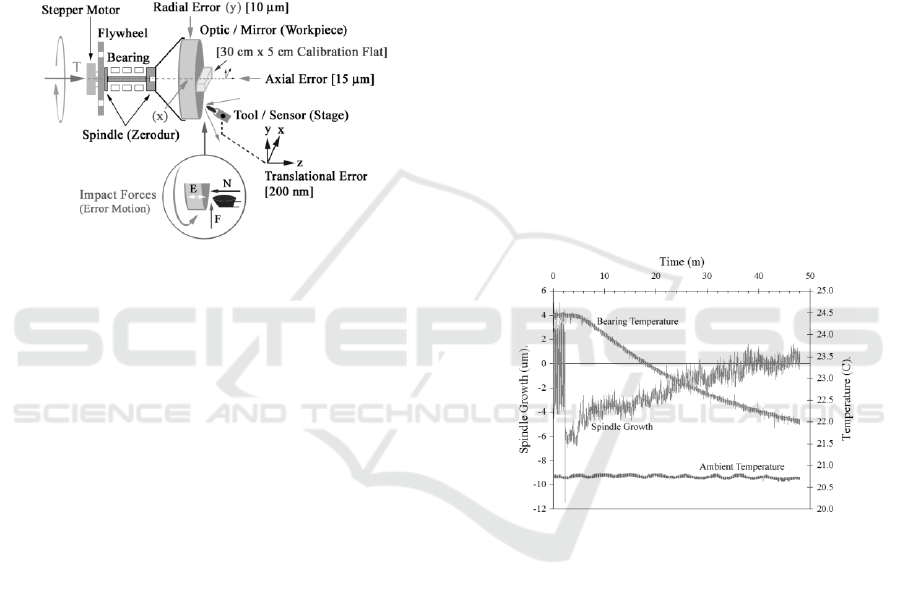
integrated systems in gravitationally levelled,
vibration isolated, and temperature controlled
environments for rotational and translational
stability, approaching multi-100 nm error motion. A
typical machine tool will operate with pressurized
fluid-lubricated bearings supporting the spindle and
the track to maintain uniform motion for high
accuracy. These tools are provided with operational
routines and techniques to match their specifications,
and it is beneficial for the operator to periodically
measure and monitor performance to maintain
repeatable product integrity and yield.
Figure 6: Axial and radial error measurement geometry on
the workpiece, and translational error on the cutting tool
holder stage. The calibration flat replaces the optic.
The measurement configuration for axial, radial,
and translational error motion is shown in Figure 6.
A cylindrical work piece is clamped to the spindle in
an appropriate manner to ensure rigid coupling, with
static preadjustment of its relative position to “true”
its surfaces to the spindle and to the tool holder, and
thereby reduce error. Typically the front planar
surface and the circumferential cylindrical surface
are then pre-machined (few µm of removal) to
conform workpiece geometry in roundness and
planarity to the dynamic circular motion of the
spindle and linear motion of the cutting tool,
respectively. The cutting tool and the sensor are
mounted on a holder stage with translational
freedom and nanopositioning capability as required.
Mechanical and thermal characteristics of the
spindle air-bearing assembly, and translational and
rotational accuracy of a precision machine tool were
examined in the triangulation-sensing configuration
(Figures 5a and 5b) to study the performance of the
tool and the sensor. A sensor was placed on axis,
parallel to the spindle, which operates free running
(100 rpm for approximately 30 min) to stabilize
thermally. The vibratory axial error motion on this
unit in operation is approximately 3 µm (Figure 7).
The rotating spindle exerts paraxial torque, which
preferentially repositions the spindle within the
bearing encasement, in an unstable axial position, in
the direction of the torque vector.
The spindle rotation was next instantly powered
down, and the sharp transition in the data at 3 min.
indicates rapid deceleration associated with loss of
power, and an axial torque-free realignment of the
spindle position within the air bearing encasement.
The spindle dynamic-to-static torque offset is 6 m
equivalent to the amplitude of the spindle axial error
motion. It now commences resting passively,
balanced axially and radially within the bearing with
uniform air suspension. The bearing temperature
was 24.5 ºC during the rotational phase, cooling off
gradually to 22 ºC, and compressing over tens of
minutes, commencing after shut down. The heat
from the bearing assembly is gradually transferred to
the spindle, which “grows” back to its position
during rotation, as the entire spindle-bearing
assembly cools and stabilizes in the environment.
This thermal growth error is slightly larger than 6
m, equivalent to the dynamic axial error, and the
torque offset. The ambient air temperature remains
steady at 20.7 ºC during these measurements.
Figure 7: Thermal analysis of a precision spindle.
2.3.2 Cutting Tool Holder-stage Accuracy
The on-axis translational accuracy and hysteresis of
the tool stage was evaluated by clamping a
commercially available 30 cm x 5 cm polished
calibration flat to the spindle chuck (Figure 6),
mounting a sensor to the tool holder, and measuring
the signal as the sensor tracks the motion of the tool
holder in a sequence of 20 steps, 125-nm each, first
retracted away from the flat, next 40 steps, 125-nm
each, moving toward the flat, and finally 20 steps,
125-nm each, retracted from the flat, back to its
original resting position. These results are shown in
Figure 8, with a detailed view in the inset. The
translational backlash (in the inset) is apparent as
progressive motion commands are given to the tool.
The overall translational motion is linear with
PHOTOPTICS 2018 - 6th International Conference on Photonics, Optics and Laser Technology
30
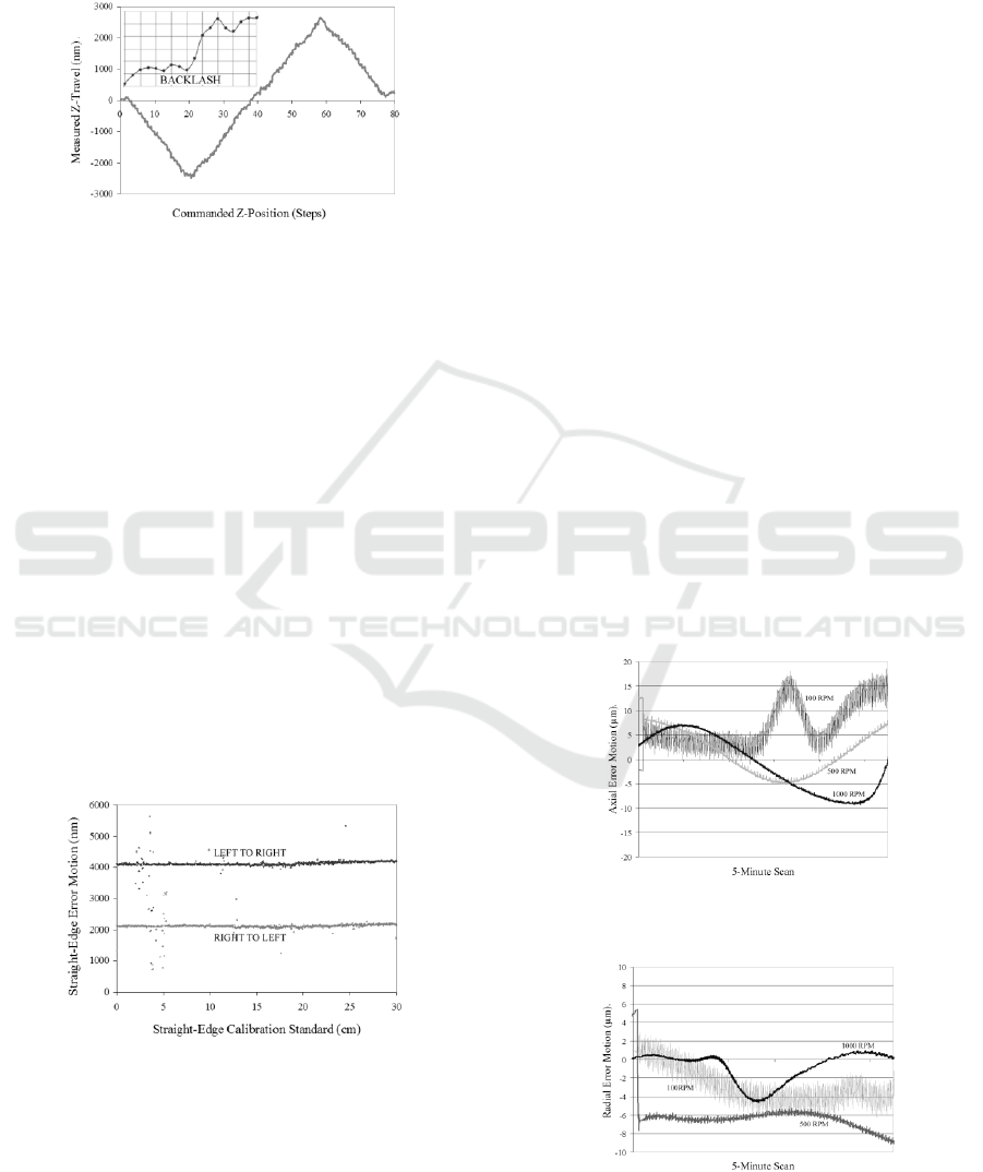
marginal error of a few 100’s nm. With the tool
traversing 10-m total roundtrip translation, from its
original resting position, through the 80-step
sequence, and returning to it, the total round-trip
hysteretic error is under 30 nm.
Figure 8: Sensor response to 80x125-nm step pattern. The
inset displays the backlash as the tool is advanced.
The translational accuracy of the tool stage,
perpendicular to the spindle axis (in the radial
direction) was also examined (Figure 9). The sensor
in this measurement was first translated across the
entire 30-cm length of the calibration flat, then offset
2 m below the original track, and next translated
back to its original position. This data indicates very
high repeatability of the tool positioning system with
error in the few 100’s nm as in the previous on-axis
measurements. A fraction of this error contains
inaccuracies of the flat and possible contamination
of the reflective surface, as is evident in the spurious
signals in the first 5 cm measurement range. The
flat also appears to have an upward bend beginning
at 18 cm, where there is an incremental trend in the
data of approximately fewer than 200 nm total.
Integrating these measurements, the triaxial x-y-z
tool-holder stage motion is shown to be accurate to
less than 200 nm with negligible hysteresis.
Figure 9: Bi-directional tracking measurements,
translating across a 30-cm calibration flat.
2.3.3 Spindle Error Motion
The dynamic axial and radial error motions of a
spindle work piece were analysed next, over a 5-
minute period of steady state rotation. The axial
measurement data set is shown in Figure 10,
evaluated at 100, 500, and 1000 rpm. The 100-rpm
axial data has rapid positional fluctuations composed
of periodic and aperiodic elements, across the entire
measurement duration, in amplitude under 6 µm,
combined with gradual axial error variation
extending to 15 µm over several minutes. The
spindle is observed to settle as the rotational speed is
increased to 500 rpm, where the rapid error noise is
reduced to less than 1 m, combined with 15-m
gradual instability over extended time. It stabilizes
much further at a speed of 1000 rpm, where the
instantaneous positional fluctuation is reduced to
less than 500 nm but the long-duration large 15-m
axial variation is persistent in the data. Radial
spindle error measurements at 100, 500, and 1000
rpm demonstrate equivalent behaviour, as seen in
Figure 11. The radial noise is comprehensively
lower than axial noise, which indicates that the
spindle as expected is radially more stable within the
bearing. The 100-rpm data has rapid periodic and
aperiodic fluctuations in the 3-µm amplitude range
combined with a slower variation of under 10 µm,
extending over duration of several minutes. The
stability improves at 500 rpm and the fast error noise
reduces to less than 1 µm. The gradual drift is less
than 5 µm over the measurement time span, or about
25% of the axial instability. The spindle, rotating at
1000 rpm, registers under a miniscule 250 nm of
high frequency noise, with 5 m of radial instability.
Figure 10: Measurements of axial error motion at 100,
500, and 1000 rpm made over a 5-minute duration.
Figure 11: Measurements of radial error motion at 100,
500, and 1000 rpm made over a 5-minute duration.
Nanoscale Non-Contact Laser Measurement of Precision Machine Tooling and Optical Surfaces
31

2.3.4 Ramifications of Spindle Error Noise
The above complement of measurements can be
integrated into an overall figure of merit of the
precision fabrication capability of this machine tool,
to estimate and project the quality of a finished
product and manufacturing yield. The limiting
factors are as outlined below, focusing on the
manner in which spindle error motion produces wear
on the cutting tool, which then induces roughness
and shape error in the machined surface. The
undesirable rotational instabilities in Figures 10 and
11, particularly approaching the 1-µm level and
larger (to 15 µm) may be associated with a
combination of factors such as torque variations
inherent in drive-motor speed inconsistencies and
spindle non-uniformities (material, warpage),
spindle inertial imbalance, unstable suspension-fluid
pressure distribution in the bearing, bearing
acoustics, multiple resonances, frictional forces,
energy transfer of the spindle to the casing,
insufficient machine tool vibration isolation,
gravitational level imbalance, thermal gradients and
non-uniform heat dissipation, and various other stray
factors. An associated factor is that instability at a
given point along the inertial axis of the spindle may
in reality be smaller in amplitude than the
measurement at the workpiece, where it is
mechanically levered to a larger amplitude - at a
pivot point along the axis within the bearing. Some
of these errors can be partially corrected since most
precision machine tools do have rebalancing
flywheels with passive adjustment to nominally
damp non-circular motion; the spindles may also be
constructed from low-expansion Zerodur to limit
thermal creep. However, a sensor-driven active
adjustment and damping system could dynamically
reduce the 15-µm slow error to less than 100 nm.
Intuitively, the best measurement areas for rotating
spindle analysis are on the workpiece, and not
directly on the spindle. All of these factors could
serve as a case study for future analysis to attain the
goal of true nanometre manufacturing.
Referring to Figure 6 (inset), the 15-µm axial and
10-µm radial spindle slow error motions represent
equivalent periodic and aperiodic error forces with
proportional counter-normal impact (E), originating
in torque error (T), and friction (F) transmitted
through the workpiece directly to the edge of the
cutting tool, which exerts normal force (N) during
the machining process; the translational error of the
tool-holder stage, and the rapid spindle error
motions (100 – 500 nm) are significantly smaller in
comparison. These combined forces (E, F, & N)
generate high friction, thermal spikes, and acoustic
shock, which produce extremely high localized
energy transfer to the cutting tool edge point-of-
contact, resulting in wear patterns in the edge profile
and its contour, limiting its usable lifetime. The
evolution of the edge profile of a cutting tool will be
explored in detail in the following section 2.3.5.
Qualitatively, the error noise data indicates that a
flat mirror surface, machined utilizing this spindle
and a fresh cutting tool, would have radially oriented
local roughness texture of depth dimension equal to
the axial fluctuations (Figure 10) of the spindle, with
relatively smaller contributions from lower radial
noise components (Figure 11), which occur in the
plane of the surface. The tool positioning error on
the order of 100 nm (Figures 8 and 9) is negligible in
comparison with the multi-m level axial and radial
fast and slow error noise of the spindle. If the
surface is a curved mirror or a lens, machined to a
pre-determined contour, the dynamic axial and radial
error-motion could result in proportional roughness
and shape variations caused by the instability of the
spindle. The axial error would induce radially
oriented roughness in the finished surface, while the
radial error could modulate this roughness texture.
These two error factors would combine and
contribute localized geometric modulations to the
shape of the surface as the contour is machined. As
with any large mechanically driven periodic system
at low-rpm operation, the axial and radial data
exhibit considerable inertial imbalance and potential
low frequency resonances in the tool. These
instabilities are damped at much higher rotational
rates, producing a relatively smooth cutting
operation. The machining of precision mirrors,
lenses, and flats requires careful consideration of
multiple factors, and evaluation of tool performance
at various speeds to determine the most suitable
operational parameters for the highest quality optical
products.
This complement of measurements and analysis
has additional applications: it can be utilized for
evaluating and optimising spindle and stage design,
implementing motion stability, damping resonances,
streamlining bearings, improving vibration isolation,
and reducing thermal gradients – all important
factors in the design and manufacture of nanometre
precision machine tools. It can also be utilized to
determine the optimal operating points for spindle
rotation, bearing fluid pressure, cutting tool depth
and feed, coolant flow, temperature, and machine
tool stability, and thus shorten the decision making
process leading to nanometre surface and shape
quality with high yield.
PHOTOPTICS 2018 - 6th International Conference on Photonics, Optics and Laser Technology
32
2.3.5 Diamond Cutting Tool Edge Profile
The next measurement in our evaluation sequence is
the cutting tool profile, and the progression of wear
during the machining operation. We focus
particularly on precision single-point diamond
turning (SPDT), utilizing commercially available
diamond cutting tools, for the fabrication of
precision mirrors and optics. These tools are
specified in terms of their contour (nose) radius,
cutting point transverse edge radius, edge roughness,
edge roundness, edge straightness, cutter angle, and
rake angle. The primary measurement of interest in
SPDT is the edge contour, as related to the nose
radius, since edge wear is directly correlated to
finished surface quality. Among various tool
parameters, contour wear is a good figure of merit,
and is directly dependent on usage duration, cutting
depth, spindle and stage error motions, thermal
gradients originating in frictional forces in the
cutting process, machining parameters such as
rotational speed and feed rate, surface material
properties, and the quality of the diamond crystal.
Edge contours on diamond tools were examined, one
freshly manufactured and another measured after its
utilization to form multiple lenses. The two tools
had zero rake angles, edge radius on the order of < 2
µm, 60-degree cutter angle, and contour radius of
0.2 mm. These diamond tools are fabricated by
polishing with progressively finer diamond particles
in controlled processes. They may contain intrinsic
crystalline defects and sub-surface damage induced
during fabrication.
Figure 12: Contour of a used diamond tool showing wear
grooves across the edge. The inset is a fresh tool.
The fresh tool was measured at the cutting point,
and the data shown in Figure 12 (inset) indicates
pristine edge quality, and smooth rake. The local
radius conforms to the manufacturer specification of
0.2 mm with minimal edge roughness and no visible
edge defects. The edge straightness also appears to
be uniform, without any manufacturing artefacts
such as polishing striations across the edge. The
tool utilized in manufacturing optical lenses has
multiple features of interest, resulting from wear,
including a modulated edge-contour profile
descending into deep furrows which span from the
rake face downwards, into the base. The regions of
modulation, have dimensions of a few to 10 µm,
superimposed on the original edge. The multi-µm
waviness of the edge contour indicates that spindle
error motion (which is of equivalent multi-µm
oscillation) is a major contributing factor in this
degradation. In SPDT, the error motion induces
equivalent periodic high impact forces on the cutting
tool edge within its microscopic area of contact with
the surface, typically on the order of 2-µm (width) x
10-µm (cutting arc) or less (Figure 6, inset). These
error-noise forces in combination with frictional
forces, acoustic shock, and thermal gradients during
machining perturb and damage the cutting tool edge
at its points of weakness: defect sites, its polish
roughness structure, and its subsurface damage. The
wear regions along the contour appear to have
become progressively deeper with usage, rendering
the cutting edge unusable. This cutting tool will
inevitably leave these imprints on the machined
surface, resulting in a poor quality product with
noticeable optical imperfections and local shape
irregularities. In combination with all of the
measurements and discussion in Section 2.3.4 the
overall quality of a machined surface utilizing this
cutting tool, at low rpm, would not result in optical
quality surfaces and shapes.
2.3.6 Surface, Defect, and Thin Film Data
Optical scatter is routinely utilized to examine
smooth surfaces and to identify defects in the optics
and the semiconductor industries, including thin
films, and multi-layer and photoresist-patterned
substrates. The geometrical arrangement to perform
these functions is shown in Figure 1. A detector is
positioned to the surface, oriented to capture scatter
radiation in a solid angle, defined by the angle of
incidence and the polarization of the input beam.
Since non-specular scatter is typically of low
intensity for smooth surfaces, the detector is coupled
to low noise, high gain electronics, and may also
include capability to select a particular polarization
to enhance feature-to-background sensitivity. The
nanometre scanning stage combined with software
processing can produce contrast-enhanced images of
surface structure and roughness, defects, and sub-
surface damage. Figure 13 shows the scatter image
Nanoscale Non-Contact Laser Measurement of Precision Machine Tooling and Optical Surfaces
33
of a diamond-turned Si surface in a 50m x 50m
field. In the machining process, the spindle operated
at 1000 rpm, and a 1.5-mm diamond tool was
advanced in 3-µm steps/rev, with 1.3-µm removal,
and impressed corresponding indentations on the Si
surface in a regular pattern; the total surface area of
the Si-wafer section was 1 cm
2
and the tool edge
profile was unknown. The surface is linear along
the y-axis but has large irregular shape inaccuracy,
on the order of 10 - 25 µm, along the x-axis,
perpendicular to the grating, equivalent to and
perhaps caused by error motion as the cutting tool
traverses the surface (See discussion in Section
2.3.4). This data indicates that if a large optic or
mirror was manufactured utilizing this machine and
cutting tool combination, µm-scale surface and
shape irregulaties would undoubtedly occur in the
finished product. In general, to quantify similar
surface errors, the cutting tool and a sensor could be
mounted on identical arcuate positions on the holder
(Figure 6). It would then be possible to first cut the
surface, and then measure its contour to determine
its accuracy within limits of the error noise of the
machine tool.
Figure 13: 50m x 50m scatter image of diamond-turned
Si showing local cutting tool indentations and overall
shape error.
Perfectly smooth planar polished surfaces were
also measured but displayed no interesting features
related to microstructure and defects, beyond a
simple flat field in the data indicating that the entire
scatter profile was confined to the specular region
with minimal Lambertian haze and no detectable
offset scatter components. This data was verified by
AFM measurements and analysis in the identical
vicinity of the surface.
We progress to examining the scatter features of
a defect. A commercially available polished quartz
blank was scanned with the same parametric
settings, and the data is shown in Figure 14. The
data contains several observable features: low
frequency wave-like roughness oriented
perpendicular to the x-axis of spatial period about 10
µm in the foreground. Towards the rear of the
sample the structure appears to be two-dimensional,
oriented randomly along both axes of 5-10 µm
dimensions, and includes peripheral geometry of a
second defect in the far corner. The defect pit
(identified in the semiconductor industry as a crystal
originated pit or COP; see inset for AFM image) in
the centre is approximately 15 µm in diameter, and
produces scatter, which indicates the presence of
some shallow vertical projections in the range of a
few micrometers forming concentric rings. The
inner ring has wavelike rim structure, while the
surrounding ring appears somewhat regular and
shallow. The defect also appears to have an internal
bridge, spanning the pit bisecting it parallel to the y-
axis.
Figure 14: Defect on quartz surface (50m x 50m)(L).
The surface structure appears to be composed of wave like
patterns with particular orientation. AFM image of a
similar defect and surface structure on the same sample is
shown (R).
In a final measurement, a composite 200-nm (50-
nm Cr and 150-nm Au), 75 µm x 75 µm thin film
pad, deposited by e-beam evaporation on a Si wafer,
was imaged to examine the scatter produced by the
structure of the film, the edges, and the corner. The
data is shown in Figure 15 and reveals
compositional information about the film, in greater
detail than could be observable by diffraction-
limited high-resolution optical microscopy. The
200-nm total film thickness is identifiable, as
indicated on the data, despite scaling to
approximately only 25% of the wavelength of
optical beam, and indicating very good depth
sensitivity of the scatterometer-triangulation
technique. The darker base region of the film is very
likely low-reflectivity Cr material, while the brighter
scatter data in the upper region is associated with
PHOTOPTICS 2018 - 6th International Conference on Photonics, Optics and Laser Technology
34
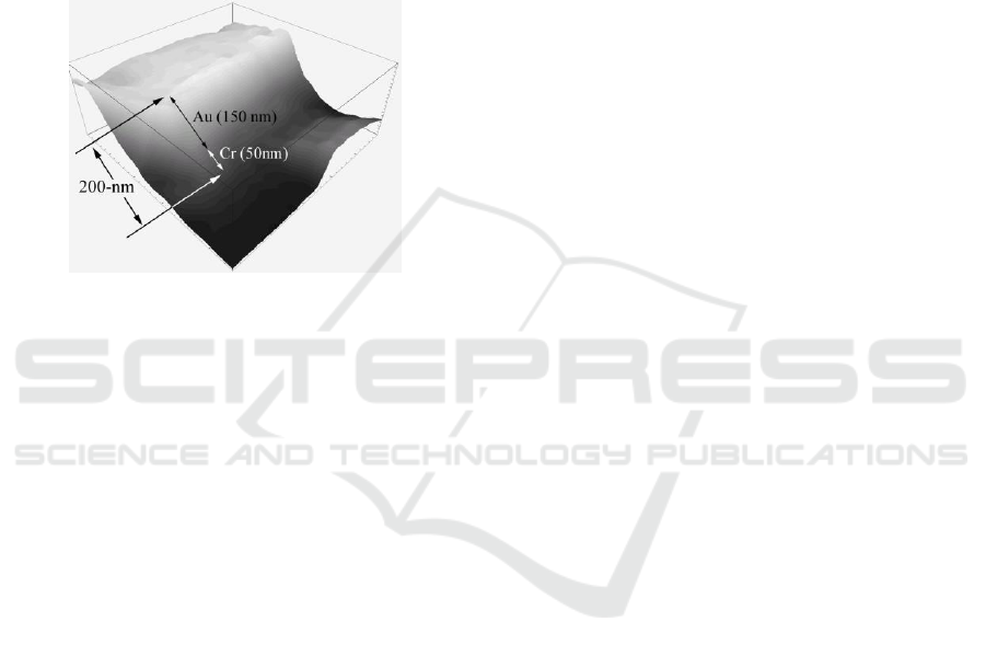
highly reflective Au. The surface of the film
appears to have randomly oriented two-dimensional
fine grain structure in the spatial frequency range of
a few micrometers laterally but extending only a few
10’s of nanometres in roughness vertically,
remarkably just under 3% in dimensional
comparison with the sensing wavelength. These
appear to be islands of molecular nucleation forming
crystallite fractals of the Au material, generated
progressively as the film is deposited. Some of this
structure may also include the underlying structure
of the Cr film.
Figure 15: 200-nm Cr-Au film on Si. The film thickness is
as shown, and the surface of the film appears to indicate
structure formed by nucleation.
There is a uniform ridge along the upper
peripheral edges of the film, related to the
photoresist-mask pattern utilized in the lithographic
lift-off fabrication process. Similar dielectric and
metal thin films are routinely deposited on optics
(anti-reflection coatings) and semiconductor wafers
(device connections and contacts), whose structure
and function could be examined by this technique.
3 CONCLUSIONS
Laser triangulation combined with detection by a
sub-nanometre resolution sensor is presented as a
versatile, contact-free, non-invasive method to
monitor and evaluate ultra-precision machine tool
operation, and to examine the surface and shape
quality of µm-size to meter-size optical and
semiconductor products to accuracy of less than 200
nm, and potentially approaching 10 nm. The
thermal stability, axial torque displacement, spindle
“growth”, tool holder stage error and hysteresis, and
the axial and radial error motion of a precision
machine tool spindle were resolved with this
apparatus in the range of < 100 nm to several m. A
diamond cutting tool edge had 10-µm wear patterns,
which developed after multiple usage cycles,
originating in spindle error motion. An SPDT Si
surface was shown to have indented lines equivalent
to the machining settings, with large overall 10 - 25
µm shape variations. This set of measurements and
analysis could be utilized to design nanometre
precision machine tools, optimise critical
components like the spindle and the bearing,
facilitate vibration isolation, and select operating
parameters to fabricate products with high quality
and large yield. Textured surface structure with
defects and internal defect structure were identified
on a quartz optical flat. Finally, a thin Cr-Au film
was examined, and the 200-nm thickness of the film
is easily identifiable together with approximately 20-
nm fractal nucleation structure on the surface of the
film. We have demonstrated the versatility,
adaptability, and reliability of this technology for
use in the manufacture of optical, semiconductor,
and other industrial products manufactured from a
multitude of materials, regardless of size.
ACKNOWLEDGEMENTS
Financial and/or technical assistance for this work
was provided from several sources at various times,
including the US Naval Research Laboratory,
California Institute of Technology, US Air Force,
NASA – Jet Propulsion Laboratory, the Livermore
Laboratory, the National Research Council, and E.F.
and B.F. Soãres.
REFERENCES
Azzam, R., and Bashara, N., 1999. Ellipsometry and
Polarized Light, Elsevier.
Heavens, O., 1955. Optical Properties of Thin Solid Films,
Dover.
Church, E., Jenkinson, H., and Zavada, J., 1979.
Relationship between Surface Scattering and
Microtopographic Features, Optical Engineering 18
(2).
Longuet-Higgins, M., 1957. Statistical Properties of an
Isotropic Random Surface, Phil. Trans. A, 250.
Stover, J., 1995. Optical Scattering, SPIE Optical
Engineering Press. Washington, 2
nd
edition.
Bohren, C., and Huffman, D., 1998. Absorption and
Scattering of Light by Small Particles, John Wiley.
Sze, S., 1981. Physics of Semiconductor Devices, John
Wiley, 2
nd
edition.
Horowitz, P., and Hill, W., 1989. The Art of Electronics,
Cambridge University Press, 2
nd
edition.
Nanoscale Non-Contact Laser Measurement of Precision Machine Tooling and Optical Surfaces
35
