
Dye-Sensitized Photoconductivity and Photovoltaic Effect in Silicon
Mikhail A. Goryaev and Rene A. Castro
Herzen State Pedagogical University of Russia, 48 Moika Emb., St. Petersburg, Russia
Keywords: Internal Photo Effect, Powdered and Monocrystalline Silicon, Dye Sensitization.
Abstract: In this paper we investigate the influence of organic dyes applied to the semiconductor surface on the
effectiveness of the direct current photoconductivity of powdered silicon and photovoltaic effect in the
monocrystalline silicon. Dyes on the semiconductor surface effectively increase the photoconductivity of
powdered samples in the dye absorption band. The effectiveness of the monocrystal sensitization is smaller
because the specific surface area of finely divided powders is several orders of magnitude larger than it is in
monocrystals. The optimum concentrations of dye molecules on the semiconductor surface for the internal
photo effect sensitization are determined. We also discuss the mechanism of the sensitization based on the
theory of non-radiative resonant inductive energy transfer.
1 INTRODUCTION
Organic dyes effectively sensitize the
photoconductivity and photolysis in broad-band
semiconductors (ZnO, AgHal, TiO
2
, etc) in the dye
absorption range (Akimov, et al, 1980, Goryaev,
2013). In the silver halide photography dye
sensitization is the most effective method of varying
the sensitivity level and spectrum of photographic
materials (James, 1977). Photoelectrochemical cells
based on the dye-sensitized titanium dioxide provide
an alternative to silicon solar batteries (Gratzel,
2003). The thickness of solar cells based on
crystalline silicon must be hundreds of microns,
because the extinction coefficient of the
semiconductor is relatively low in the range of
indirect electron transitions (Alferov, et al, 2004,
Afanasyev, et al, 2011, Duffie and Beckman, 2013).
Modern electron photography systems have the
silicon CCD matrices as image sensors in (Boyle,
2010), and using light filters for color separation
system leads to the loss of energy and valuable
information (Goryaev and Dudnikov, 1990). In the
present study we investigated the internal photo effect
in silicon and the influence of the application of
organic dyes to the semiconductor surface on its
effectiveness.
2 EXPERIMENTAL
Silicon powdered samples with micron-sized
microcrystals and flat monocrystals of 1-2 cm
2
with a
thickness of 0.5 mm were used for the investigation.
The semiconductor surface was covered with dyes
from the ethanol solution with a definite
concentration by means of a natural evaporation of
the solvent at room temperature. The direct current
(DС) photoconductivity measurements were
performed in special surface type cells for
investigating the electro-physical properties of
powder semiconductors (Povkhan, et al, 1974), in
which the sample in the pellet form was pressed to a
quartz plate under constant pressure (approx. 10
kg/cm
2
). The quartz plate was covered with a raster
of platinum electrodes; the distance between the
electrodes was 0.1 mm, and the effective length of
electrodes was 80 mm. The photocurrent
I
ph
measured under the conditions of a constant sweeping
electric field was normalized to number of light E
(Goryaev, 2015). The method used for the
investigation of the monocrystalline samples was the
measurement of the photo-EMF at the modulated
irradiation (Akimov, 1966). To estimate the
effectiveness of the photovoltaic effect, the measured
signals
U
ph
were normalized to number of light
quanta E.
130
Goryaev, M. and Castro, R.
Dye-Sensitized Photoconductivity and Photovoltaic Effect in Silicon.
DOI: 10.5220/0006525701300135
In Proceedings of the 6th International Conference on Photonics, Optics and Laser Technology (PHOTOPTICS 2018), pages 130-135
ISBN: 978-989-758-286-8
Copyright © 2018 by SCITEPRESS – Science and Technology Publications, Lda. All rights reserved
3 RESULTS AND DISCUSSION
3.1 DC Photoconductivity
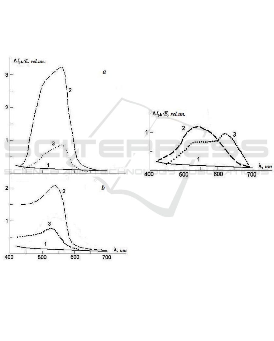
The photoconductivity spectra of powdered silicon
are shown on figures 1 and 2: the undyed sample
(curve 1) and the samples with the dyes applied to the
semiconductor surface (curve 2). The results
demonstrate that the photoconductivity of dyed
samples in the absorption range of the dyes (curve 2,
Fig. 1 and Fig. 2) is higher than the photoconductivity
of the original silicon sample (curve 1, Fig. 1 and 2)
by more than an order of magnitude.
Figure 1: Photoconductivity spectra of undyed silicon (1)
and samples dyed with Rhodamine 6G (a) and Erythrosine
(b) with concentrations of 10
-4
Mole/g of Si (2) and 2×10
-4
Mole/g of Si (3) with concentrations of 10
-4
Mole/g of Si
(2) and 2×10
-4
Mole/g of Si (3).
The increase in photoconductivity in the
absorption range of the dye cannot be related to the
carrier generation in the dye layer because the dark
conductivity of both the powdery dye layers and the
thin dye films deposited from a solution on a quartz
plate with electrodes is several orders of magnitude
smaller than the conductivity of undyed silicon
samples, while the photoconductivity is absent
altogether. This circumstance explains the decrease in
the photocurrent for the dye deposited in a large
amount on the semiconductor surface (Goryaev,
2015).
The magnitude of the observed photocurrent
sensitization effect depends on the amount of dye
applied to the semiconductor surface non-
monotonely: when the dye concentration is increased,
the photoconductivity at first increases and then
decreases (curves 2 and 3, Fig. 2). The decrease in the
photocurrent when the large amount of dye is
deposited on the semiconductor surface is explained
by the fact that a solid insulating dye film is formed
on silicon, and it hinders the transition of charge
carriers among the microcrystals. The optimum
concentration of dye molecules on the semiconductor
surface for the photocurrent sensitization of
powdered samples is about of 10
-4
Mole/g of Si.
Figure 2: Photoconductivity spectra of undyed silicon (1)
and samples dyed with Crystal Violet with concentrations
of 10
-4
Mole/g of Si (2) and 2×10
-4
Mole/g of Si (3).
The investigation of photoconductivity spectra
shows the interesting results for the samples with the
dye crystal violet applied to the semiconductor
surface (Fig. 2). On increasing dye concentration not
only a decreasing photoconductivity in the dye
absorption band due to the insulating dye film
formation is observed, but an additional absorption
band appears in the long-wave region (curves 2 and
3, Fig. 2). This fact may be explained by the J-
aggregates formation at the large amount of dye on
the semiconductor surface. The absorption band of
dye J-aggregates lies in the longer wave region and
their sensitization effectiveness is larger than that for
the dye in a non-aggregated state (James, 1977).
3.2 Photovoltaic Effect
For the monocrystalline silicon the spectral
sensitization of condenser photo-EMF is also
Dye-Sensitized Photoconductivity and Photovoltaic Effect in Silicon
131
observed in the absorption band of the dye (curves 2
and 1, Fig. 3). In comparison to powdered silicon the
magnitude of the sensitized photo effect in silicon
monocrystals is significantly smaller than in
polycrystalline samples (Goryaev, 2017). This is a
consequence of the fact that the specific surface area
of monocrystals is several orders of magnitude
smaller than in microcrystals of finely divided
powders. It should also be noted that during a
characteristic absorption the absorption and carrier
generation happens rather deep in the crystal because
of a small extinction coefficient of silicon. The role
of near-surface photoelectron generation increases
during the light absorption by dyes because the
efficient energy transfer radius during the dye
sensitization is several nanometers large (Akimov, et
al, 1980). The thickness of monocrystals is very
significant, therefore the number of such near-surface
photoelectrons is small in comparison with the
carriers generated due to the characteristic absorption
in the volume of the semiconductor.
Figure 3: Photo-EMF spectra of undyed silicon
monocrystals (1) and samples dyed with Rhodamine 6G
with dye molecule concentrations of 30 nm
-2
(2) and 60 nm
-
2
(3).
The magnitude of the observed photo effect
sensitization depends on the amount of dye applied to
the semiconductor surface non-monotonely as well:
when the dye concentration is increased on
monocrystals the photo-EMF at first increases and
then decreases in an absorption band of the dye
(curves 2 and 3, Fig. 3). Dye sensitization is observed
at the optimum concentration of dye molecules on the
monocrystal surface about of 30 nm
-2
. Taking into
account the fact that the surface density of molecules
in the dye monolayer is 0.7-1.4 nm
-2
(James, 1977),
the optimum thickness of the dye film formed on the
monocrystal surface is around 30 monolayers or 10-
15 nanometers. As the length of the efficient radius of
energy transfer at the spectral dye sensitization is 5-7
nanometers (Akimov, et al, 1980), part of the energy
absorbed by the dye does not reach the semiconductor
for the larger film thickness. Besides, increasing the
film thickness increases the role of the intramolecular
energy conversion rate on the vibrational and
rotational degrees of freedom during light absorption
by the dye. Those processes lead to the filter effect in
an absorption band of the dye applied on the solid
surface, as it is observed for the photophysical and
photochemical processes in the dye – aluminum
hydride system (Goryaev and Pimenov, 1975,
Goryaev, 1980; 2000).
3.3 Mechanism of Sensitization
The efficiency of spectral sensitization for the
photoelectron formation in a solid after the light
absorption by the dye applied on the surface is
determined by the following ratio:
P
s
= P
a
.
P
tr
.
P
ph
, (1)
where P
a
– the efficiency of absorption determined
by the dye extinction coefficient and its
concentration; P
tr
– transfer efficiency of excitation
energy from dye to semiconductor; P
ph
– the
efficiency of photoelectron formation in a solid as a
result of the excitation energy transfer from dye.
Some processes occur in the dye-semiconductor
system during light absorption by the dye. After the
dye photoexcitation non-radiative and radiative
electron transitions can realize in molecules. The
possibility of electron excitation energy exchange
between the vibrational and rotational degrees of
freedom and the rate of the internal energy
degradation are determined by the rigidity of the dye
molecule skeleton. For dyes applied on the solid
surface the molecular structure becomes more rigid
and intramolecular conversion probability becomes
insignificant. As result the luminescent quantum yield
of dyes is measured in tens of percent on the
dielectrics surfaces (Goryaev, 1980; 1981; 1997,
Goryaev and Smirnov, 2015). But the luminescence
is completely absent on metals, narrow-band
semiconductors and well-sensitizable photosensitive
broad-band semiconductors (for example, silver
halides and zinc oxide) because of the effective
photoexcitation energy transfer from dyes to the
solids (Akimov and Goryaev, 1984).
After the light absorption the photoexcitation
energy received by the dye can be transferred to the
semiconductor, be observed as luminescence and
degrade within the molecule with the corresponding
transition constants k
1
, k
2
and k
3
. Transfer efficiency
PHOTOPTICS 2018 - 6th International Conference on Photonics, Optics and Laser Technology
132
of the excitation energy is determined by the
following ratio:
(2)
The intramolecular energy conversion rate k
3
becomes insignificant when compared to k
1
and k
2
for
the majority of dyes applied on the solid surface
because of the hardening of the molecule structure.
Therefore the luminescence becomes the main
competing process with the effective electronic
excitation transfer to the semiconductor. The
fluorescent state lifetimes of dyes applied on the solid
surface are 10
-11
– 10
-10
s (Akimov and Goryaev,
1984, Goryaev, 2013), and photoexcitation transfer
rate constant k
1
in effectively sensitized
semiconductors exceeds 10
12
s
-1
(Akimov, et al, 1980,
Goryaev, 2013), so the quantum effectiveness of the
photophysical and photochemical processes
sensitization in the semiconductor
approaches unity
under such circumstances.
According to the theory of non-radiative resonant
inductive energy transfer, the transfer probability
depends on the overlap integral of the donor
luminescence spectrum and the acceptor absorption
spectrum (Ermolaev, et al, 1996):
(3)
In equation (3): q
0d
and
0d
– are, accordingly, the
quantum yield and duration of luminescence decay of
the donor in the absence of quenching, I
d
– quantum
radiation spectral density of luminescence,
a
–
molar decimal absorption coefficient, R – distance
between the donor and the acceptor, n – the
environment refractive index,
– wave number, C –
constant.
Local electronic states of the forbidden band play
the role of the energy acceptors in broad-band
semiconductor sensitization (Akimov, et al, 1980,
Akimov and Goryaev, 1984, Goryaev, 2013). The
existence of such local states in the semiconductors
capable of accepting energy from the dye is the main
reason for the luminescence quenching in these
systems. The integrated density 10
9
-10
10
cm
-2
of the
surface states occupied by electrons is sufficient for
the complete luminescence quenching (Goryaev,
2013). This is the necessary requirement for the
sensitization of broad-band semiconductors. Such
surface states are responsible for the weak absorption
and photoconductivity in the impurity region of the
semiconductors. The dyes applied on the solid surface
provide the spectral sensitization of the photophysical
and photochemical processes in the semiconductors
because of increasing the absorption in this region.
In silicon this spectral region corresponds to
electronic transitions from the valence band to the
conduction band. The densities of states in these
bands are quite sufficient for the complete dye
luminescence quenching because of accepting the
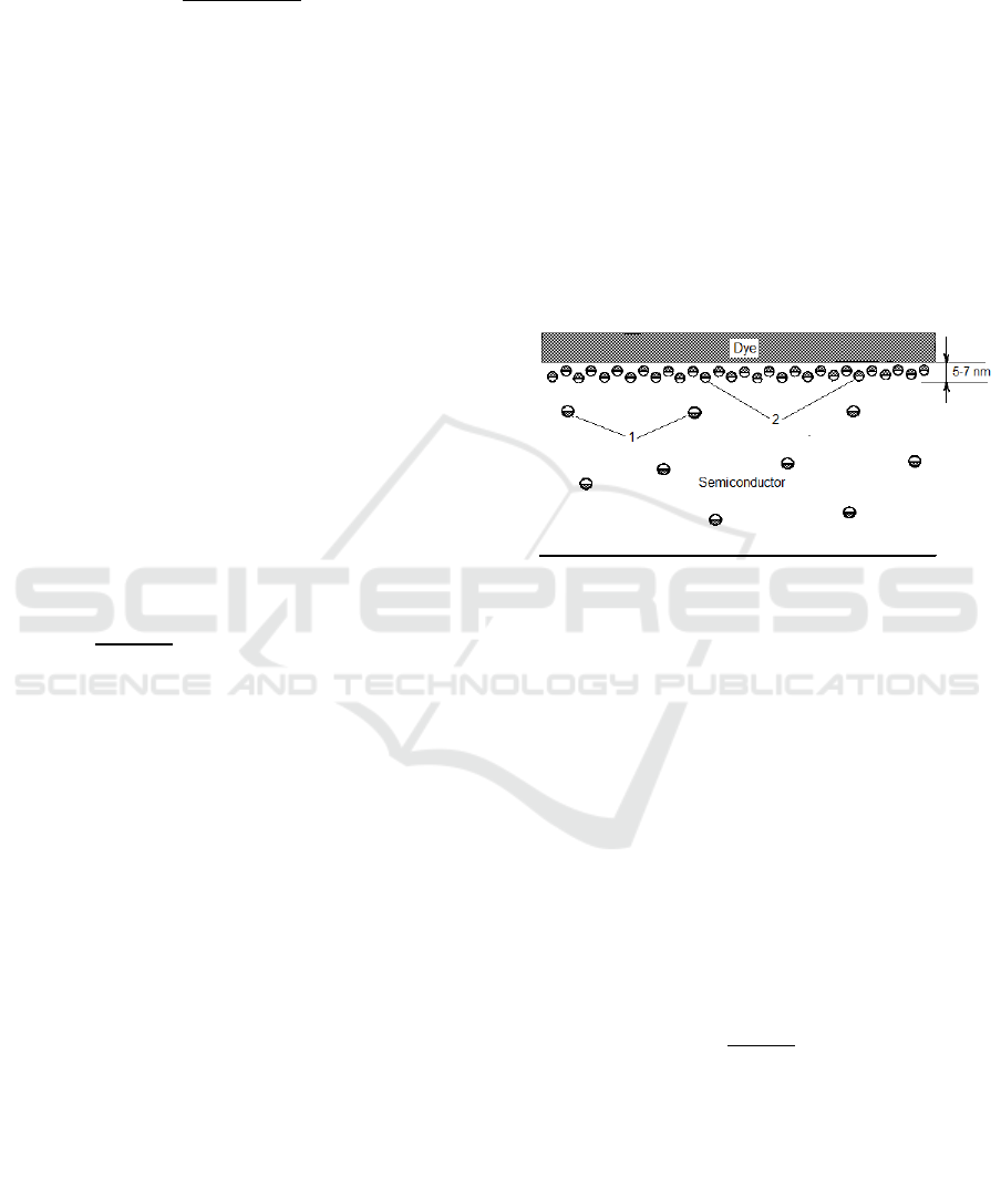
photoexcitation energy. The intrinsic light absorption
by the semiconductor is formed by indirect electronic
transitions, and free carriers obtained by the intrinsic
absorption are generated in the volume of the
semiconductor. The near-surface free carriers
generation during the light absorption by dyes
produces a significant increase in the efficiency of the
photoelectric effect (Fig. 4).
Figure 4: The generation of free carriers in the volume of
the semiconductor due the intrinsic absorption in silicon (1)
and in the subsurface region due the energy transfer from
the dye (2).
The sensitization process efficiency after the
transfer of excitation from a dye to the semiconductor
is determined by the fate of an electron appearing in
the semiconductor conductivity band. This electron
may remain free for a sufficient period of time,
enabling the sensitized photoeffect, or may quickly
recombine. If the free carriers are formed with a
constant k
4
and recombination of carriers in a
semiconductor occurs with constant k
5,
the
effectiveness of the photoelectron formation in a solid
after electronic excitation transfer is determined by
the formula:
4
45
.
ph
k
P
kk
(4)
The additional reason for the large differences of
sensitized photoelectric effect in monocrystalline and
powder silicon is that photo-EMF has both drift and
diffusion components (Akimov, 1966). If the
spectrum of the drift component repeats the
photoconductivity spectrum, the diffusion photo-
EMF is determined not by the concentration of
carriers but by their gradient. Depending on the
Dye-Sensitized Photoconductivity and Photovoltaic Effect in Silicon
133

subsurface band bending, drift and diffusion currents
have different signs. At the dye – silicon
heterojunction the change of photopotential character
during illumination in different spectral regions was
discovered (Komolov, et al, 2006). The subsurface
band bending in semiconductors can be controlled by
an external electric field or an additional illumination
(Akimov, 1966), as well as the adsorption of the
electron-acceptor and electron-donor molecules on
the semiconductor surface (Pimenov and Goryaev,
1976).
4 CONCLUSIONS
Observed effective dye sensitization of the internal
photoelectric effect in silicon can be used in such
semiconductor devices for converting the light energy
into electric energy as solar panels or image sensors
in modern electronic photography systems. In the
case of silicon solar batteries increasing the near-
surface free carriers generation may decrease the
thickness of cells. The application of dye sensitization
in CCD matrices will enable the improvement of the
color separation system during the recording of
colored images as in traditional silver halide
photography. Selecting appropriate dyes to provide
an effective increase in sensitivity in the required
spectral range instead of using light filters can
decrease losses of energy and of valuable information
in electronic photography.
ACKNOWLEDGEMENTS
This research was supported by the Ministry of
Education and Science of the Russian Federation
(Project No. 3.5005.2017/BY).
REFERENCES
Afanasyev, V.P., Terukov, E.I., Sherchenkov, A.A., 2011.
Thin Film Solar Cells Based on Silicon. State
Electrotech. Univ. St. Petersburg.
Akimov, I.A., 1966. The internal photoeffect investigation
in semiconductors by the condenser method. In Soviet
J. Optical Technology. V. 33. No 5. P. 248-257.
Akimov, I.A., Cherkasov, Yu.A., Cherkashin, M.I., 1980.
Sensitized Photoeffect. Nauka. Moscow.
Akimov, I.A., Goryaev, М.А., 1984. Photoprocesses in
semiconductors with adsorbed dye. In Zh. fizicheskoi
khimii, V. 58, No 5. P.1104-1107.
Alferov, Zh.I., Andreev, V.M., Rumyantsev, V.D., 2004.
Solar Photovoltaics: Trends and Prospects. In
Semiconductors. V. 38. No 8. P. 899-908.
Boyle, W.S., 2010. Nobel Lecture: CCD—An extension of
man’s view. In Rev. Modern Physics. V. 82, fasc. 3. P.
2305—2306.
Duffie, J.A., Beckman, W.A., 2013. Solar Engineering of
Thermal Processes, John Wiley & Sons, Inc. New
York.
Ermolaev, V.L., Bodunov, E.N., Sveshnikova, E.B. 1996.
Inductive-resonant mechanism of nonradiative transi-
tions in ions and molecules in condensed phase. In
Physics-Uspehi, V. 39. No 3. P. 261-282.
Goryaev, М., 2013. Physical fundamentals of solid state
photochemistry. Photolysis of inorganic solids.
Lambert Acad. Publ., Saarbrucken.
Goryaev, М.А., Dudnikov, Yu.A., 1990. Electronic and
hybrid imaging systems. In Zh. nauchnoi i prikladnoi
fotografii i kinematografii. V. 35. No 5. P. 386-394.
Goryaev, М.А., 2015. Spectral Sensitization of Internal
Photoeffect in Silicon. In Izvestiya Rossiiskogo
gosudarstvennogo pedagogicheskogo universiteta. V.
176. P. 71-75.
Goryaev, М.А., 2015. Dye sensitization of
photoconductivity of polycrystalline silicon. In Russian
J. Physical Chemistry A. V. 89. No. 12. P. 2320-2321.
Goryaev, М.А., 2017. Dye Sensitization of Silicon. In
International J. Modern Engineering Research. V. 7.
No 5. P. 39-43.
Goryaev, М.А., 1980. Method of determining the
luminescence spectra of powdered systems. In Soviet
Technical Physics Letters, V. 6. No 9. P. 484-485.
Goryaev, М.А., 1981. Quantum yield and luminescence
spectra of dyes in the adsorbed state. In Optics and
Spectroscopy. V. 51. No 6. P. 562-564.
Goryaev, М.А., 1997. Spectral dependence of the
luminescence quantum yield of adsorbed dyes. In
Optics and Spectroscopy. V. 82. No 5. P. 723-725.
Goryaev, М.А., Smirnov, A.P., 2015. Luminescence of dye
adsorbed on silver stearate and sensitization of
photothermographic materials. In Izvestiya Rossiiskogo
gosudarstvennogo pedagogicheskogo universiteta. V.
173. P. 50-54.
Goryaev, М.А., Pimenov, Yu.D., 1975. The action of an
electric field on photochemical processes in aluminum
hydride. In Soviet J. Optical Technology. V. 42. No 9.
P. 538-541.
Goryaev, М.А., 1980. Photoprocesses in aluminum hydride
with an adsorbed dye. In Optics and Spectroscopy. V.
49. No 6. P. 625-627.
Goryaev, М.А., 2000. Vacancy mechanism of the
photolysis of aluminum hydride. In Optics and
Spectroscopy. V. 88. No 1. P. 42-45.
Gratzel, M., 2003. Dye-sensitized Solar Cells. In J.
Photochem. Photobiol. C: Photochem. Rev. V. 4. No 2.
P. 145-153.
James, T.H., 1977. The Theory of the Photographic
Process, Мacmillan Publ. Company. New York.
Komolov, S.A., Gerasimova, N.B., Aliev Yu.G., et al,
2006. Photoelectronic properties of organic films on the
PHOTOPTICS 2018 - 6th International Conference on Photonics, Optics and Laser Technology
134

silicon surface. In Zh. tekhnicheskoi fiziki,. V. 76. No 7.
P. 76-80.
Pimenov, Yu.D., Goryaev, М.А., 1976. Scales of
perturbation undergone by an adsorbent-semiconductor
with adsorption of molecules of donor-acceptor type. In
Kinetics and Catalysis. V. 17. No 4. P. 899-903.
Povkhan, T.I., Demidov, K.B., Akimov, I.A., 1974. Cells
for research of electrophysical properties of powdered
semiconductors. In Pribory and Tekhnika
Eksperimenta. No 3. P. 217-218.
Dye-Sensitized Photoconductivity and Photovoltaic Effect in Silicon
135
