
Design the Structure of Vertical Multilayer Hybrid Silicon
Waveguide to Work in Anomalous Dispersion Region
Zengzhi Huang
1,2
, Shuai Yuan
2
and Jinsong Xia
2
1
School of Optical and Electronic Information, Huazhong University of Science and Technology, Wuhan 430074, China
2
Wuhan National Laboratory for Optoelectronics, Huazhong University of Science and Technology, Wuhan 430074, China
Keywords: Waveguide, Dispersion, Slot Waveguide, Silicon Photonics, Nonlinear Optical Device, Integration Optics.
Abstract: In order to decrease the dispersion of the silicon vertical slot waveguide, we propose a vertical multilayer
hybrid silicon waveguide. The optical mode distribution of the multilayer waveguide is simulated by a finite
element method. By a proper design of the waveguide parameters, the dispersion of waveguide can in the
range of ±300 ps/nm/km in 1510-1590 nm, with one zero-group-dispersion point in the C band. This
waveguide can be an alternative in on-chip nonlinear application, such as all optical signal processing.
1 INTRODUCTION
Silicon photonics has been an important branch in
modern optics. Due to its compact size and rich
nonlinear properties, silicon waveguides are
promising in on-chip signal transmission and all
kinds of signal processing. One main obstacle of the
application of silicon waveguides is its relatively
large waveguide dispersion, which induces optical
pulse broadening in signal transmission and phase-
mismatch in some nonlinear parametric process.
Conventionally, the process of efficient four wave
mixing occurs in a waveguide with anomalous
dispersion. Although the material dispersion of
crystalline silicon is large and normal, it can be
compensated by the structural dispersion through
optimization of waveguide structure parameters. For
silicon strip waveguide, broad-band anomalous
dispersion has been realized(Turner et al., 2006) and
optical parametric gain has been experimentally
demonstrated(Foster et al., 2006).
Silicon slot waveguide is proposed in
2004(Almeida et al., 2004) and broadly investigated
in the last decade(Zengzhi et al., 2015, Huang and
Xia, 2016). Combining high quality nonlinear
cladding material with silicon slot waveguide, the
hybrid slot waveguide is potential in on-chip all-
optical signal processing. A lot of researches relate
to the dispersion engineering of silicon slot
waveguides to achieve anomalous dispersion in
telecommunication wavelength to near infrared
wavelength. Most researches are based on a
horizontal slot waveguide structure, that is, the
direction of the slot is horizontal to the silica
substrate(Zhang et al., 2010b, Zhang et al., 2010a).
For vertical slot waveguides, it’s difficult to tailor
the dispersion to the anomalous region. Some
designs tailor the dispersion by shifting the slot
position off the waveguide centre of using dual-slot,
however, that leads to in some working wavelengths,
the optical field are not centred in the slot
region(Zhu et al., 2012).
In this article, we propose a novel hybrid
vertical slot waveguide structure intended to achieve
broad-band anomalous dispersion in
telecommunication wavelength and near infrared
wavelength. This novel vertical slot waveguide
structural is like a multilayer structure in horizontal
direction. By choosing appropriate low index
material, the hybrid silicon slot waveguide can have
a zero-group-dispersion wavelength in the
telecommunication region. What’s more, using this
novel waveguide, a large portion of the optical
energy contains in the low-index slot and cladding
region, which is beneficial in reducing the two photo
absorption and free carriers absorption in the silicon
layer.
2 WAVEGUIDE STRUCTURE
Before designing the waveguide structure, we first
take a look at the two familiar silicon waveguides,
channel waveguide and slot waveguide. The
294
Huang Z., Yuan S. and Xia J.
Design the Structure of Vertical Multilayer Hybrid Silicon Waveguide to Work in Anomalous Dispersion Region.
DOI: 10.5220/0006220802940297
In Proceedings of the 5th International Conference on Photonics, Optics and Laser Technology (PHOTOPTICS 2017), pages 294-297
ISBN: 978-989-758-223-3
Copyright
c
2017 by SCITEPRESS – Science and Technology Publications, Lda. All rights reserved

dispersions of both waveguides have been
investigated by previous works. It’s known that
silicon has a large and normal dispersion near
1550nm. Fortunately, silicon waveguide has a strong
confinement of light, which induces large structural
dispersion. By optimizing waveguide structure
parameters, the structural dispersion can be
anomalous dispersion and compensate the material
dispersion, thus obtaining anomalous waveguide
dispersion.
We use Lumerical mode solution software to
simulate the waveguide dispersion. The material
dispersions of silicon and SiO
2
are taken into
consideration, in the form of Sellmeier Equation.
Fig.1 shows the dispersion of a channel waveguide.
The waveguide is on a 340nm SOI substrate. The
width of the waveguide is 500nm. We can see that
there is a zero group velocity dispersion point in
1567nm. For wavelength larger than 1567nm, the
channel waveguide shows anomalous dispersion.
Figure 1: Simulated dispersion curve of a silicon channel
waveguide, with a size of 500nm × 340nm (width ×
height).
However, it’s difficult to achieve anomalous
dispersion in vertical silicon slot waveguides. Fig. 2
is the dispersion curve for a slot waveguide. The
waveguide parameters are as following, h=340nm,
W
Si
=200nm and W
slot
=100nm. The total width of the
slot waveguide is 500nm, same as the channel
waveguide calculated above. It can be seen that the
vertical slot waveguide has a large and normal
dispersion in the wavelength from 1610-1820 nm.
Compared Fig.2 with Fig. 1, we can conclude
that the insertion of the 100-nm slot in the middle of
the channel waveguide makes a big difference to the
waveguide dispersion. This is because the air slot
breaks the continuity of the electric field component
E
x
of the TE mode.
Figure 2: Simulated dispersion curve of a silicon vertical
slot waveguide. The top silicon layer thickness is 340nm.
The widths of the slot and silicon rail are 100nm and
200nm, respectively.
In order to decrease the normal dispersion of
the vertical slot waveguide, two ways are
demonstrated to be feasible. i). Design a waveguide
with larger cross section. That means increasing the
thickness of the top silicon and the width of the
waveguide. ii). Reduce the refractive index
difference between the silicon and slot region. Both
of these two ways are supposed to alleviate the
abrupt change of the optical mode induced by the
waveguide boundary.
3 MODAL PROFILE
Following these two designing principles, we
propose a vertical multilayer hybrid silicon
waveguide, shown like Fig. 3. It can be seen as a
silicon slot waveguide with a rectangular low-index
cladding. W and h denote the width and height of the
cladding, respectively. W
Si
and W
slot
represent the
width of the silicon rail and the width of the central
low index region.
Figure 3: A schematic of the vertical multilayer hybrid
silicon waveguide (in cross view).
Design the Structure of Vertical Multilayer Hybrid Silicon Waveguide to Work in Anomalous Dispersion Region
295
An optical mode simulation is performed using
the COMSOL Multiphysics software. The
simulation region is 4μm×4μm. The simulation
boundary is set as scattering boundary condition.
The waveguide parameters are W=700 nm, h=500
nm, W
Si
=100 nm and W
slot
=200 nm. The refractive
index of the low index material is set as 2.4, so the
electric field in the low index region is enhanced by
a factor of 1.45 on the Si-slot interface. The effective
index of the multilayer waveguide is 2.23 in 1550nm.
Fig. 4 is the electric field distribution of the
fundamental quasi-TE mode. We can observe that a
characteristics slot mode exists in the proposed
waveguide, in which the electric field in the low
index slot region is increased. The electric field
enhancement can also be reflected by a 2D cross line
view, as the yellow line in Fig. 4 shows.
Figure 4: Electric field distribution of the multilayer
waveguide.
Compared to the traditional silicon slot
waveguide, the multilayer vertical waveguide has
smaller W
Si
and larger
W
slot
, due to two additional
low index regions. This feature is fascinating in
nonlinear application based on silicon slot
waveguide, because the two photon absorption effect
in silicon is suppressed and it is promising to
achieve a high figure of merit (FOM)(Zhang et al.,
2015).
4 WAVEGUIDE DISPERSION
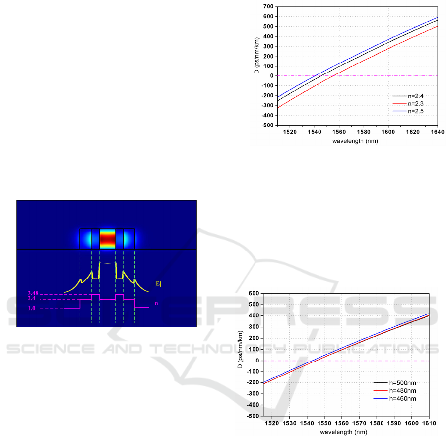
We calculate the dispersion of the multilayer
waveguide, shown as Fig.5. For low index material
refractive index n=2.4, the waveguide dispersion is
less than ±300 ps/nm/km in 1510-1590 nm, with a
zero-group-dispersion point in 1542 nm. For
wavelength longer than 1542 nm, the multilayer
waveguide have anomalous dispersion.
Figure 5: Waveguide dispersion curves for n=2.3, 2.4 and
2.5, respectively. The other parameters are W=700 nm,
h=500 nm, W
Si
=100 nm and W
slot
=200 nm.
Next we investigate how the waveguide
parameters influence the dispersion of the multilayer
waveguide. Varying n from 2.3 to 2.5, we can see in
Fig.5 that if n becomes larger, the dispersion curve
moves upwards and the zero-group-dispersion point
moves to shorter wavelength.
The waveguide height has small influence to the
waveguide dispersion. This is shown in Fig.6.
Figure 6: Waveguide dispersion curves for h=460nm,
480nm and 500nm, respectively. The other parameters
used for simulation are W=700 nm, W
Si
=100 nm,
W
slot
=200 nm and n=2.4.
The dispersion curve for various W
Si
is depicted
in Fig.7. The figure shows that W
Si
is an important
factor that decides the waveguide dispersion. For
W
Si
=90 nm, the multilayer waveguide remains in
anomalous dispersion region for the whole
calculation wavelength. However, W
Si
=120 nm, the
waveguide works in normal dispersion.
PHOTOPTICS 2017 - 5th International Conference on Photonics, Optics and Laser Technology
296

Figure 7: Waveguide dispersion curves for W
Si
=90nm,
100nm, 110nm and 120nm, respectively. The other
parameters used for simulation are W=700 nm, h=500 nm,
W
slot
=200 nm and n=2.4.
5 CONCLUSIONS
In this paper, we propose a vertical multilayer
silicon hybrid waveguide, to overcome the large
normal dispersion of the vertical silicon slot
waveguide. By proper design, the dispersion of
waveguide can in the range of ±300 ps/nm/km in
1510-1590 nm. This kind of waveguide can be as a
nonlinear optical waveguide, and find its
applications in on-chip all optical signal processing.
The multilayer waveguide provides additional
flexibility in tailoring the dispersion. A lower, flatter
dispersion can be obtained by further optimization.
ACKNOWLEDGEMENTS
This work is supported in part by the Major State
Basic Research Development Program of China
under Grant 2013CB632104 and Grant
2013CB933303, and in part by the National Natural
Science Foundation of China under Grant 61177049
and Grant 61335002.
REFERENCES
Almeida, V. R., Xu, Q., Barrios, C. A. & Lipson, M. 2004.
Guiding and Confining Light in Void Nanostructure.
Optics Letters, 29, 1209-1211.
Foster, M. A., Turner, A. C., Sharping, J. E., Schmidt, B.
S., Lipson, M. & Gaeta, A. L. 2006. Broad-Band
Optical Parametric Gain on a Silicon Photonic Chip.
Nature, 441, 960-963.
Huang, Z. & Xia, J. 2016. Sub-50-Nm Wide Slot
Waveguides with Good Optical Isolation on Silicon on
Insulator. Optical Engineering, 55, 087102-087102.
Turner, A. C., Manolatou, C., Schmidt, B. S., Lipson, M.,
Foster, M. A., Sharping, J. E. & Gaeta, A. L. 2006.
Tailored Anomalous Group-Velocity Dispersion in
Silicon Channel Waveguides. Optics Express, 14,
4357-4362.
Zengzhi, H., Zhang, Y., Zeng, C., Li, D., Nisar, M. S., Yu,
J. & Xia, J. 2015. High Confinement Factor Ridge Slot
Waveguide for Optical Sensing. Ieee Photonics
Technology Letters, 27, 2395-2398.
Zhang, L., Yue, Y., Beausoleil, R. G. & Willner, A. E.
2010a. Flattened Dispersion in Silicon Slot
Waveguides. Optics Express, 18, 20529-20534.
Zhang, L., Yue, Y., Xiao-Li, Y., Wang, J., Beausoleil, R.
G. & Willner, A. E. 2010b. Flat and Low Dispersion
In Highly Nonlinear Slot Waveguides. Optics Express,
18, 13187-13193.
Zhang, W., Serna, S., Dubreuil, N. & Cassan, E. 2015.
Nonlinear Optimization of Slot Si Waveguides: Tpa
Minimization With Fomtpa up To 4.25. Optics Letters,
40, 1212-1215.
Zhu, M., Liu, H., Li, X., Huang, N., Sun, Q., Wen, J. &
Wang, Z. 2012. Ultrabroadband Flat Dispersion
Tailoring of Dual-Slot Silicon Waveguides. Optics
Express, 20, 15899-15907.
Design the Structure of Vertical Multilayer Hybrid Silicon Waveguide to Work in Anomalous Dispersion Region
297
