
Integrated Optical Devices
Fabrication of Multimode Interference Devices in Fused Silica by Femtosecond
Laser Direct Writing
Vítor A. Amorim
1,2
, João M. Maia
1,2
, D. Alexandre
1,3
and P. V. S. Marques
1,2
1
Center for Applied Photonics, INESC TEC, Rua Dr. Roberto Frias, Porto, Portugal
2
Department of Physics and Astronomy, University of Porto, Porto, Portugal
3
Department of Physics, University of Trás-os-Montes e Alto Douro, Vila Real, Portugal
Keywords: Femtosecond Laser, Laser Direct Writing, Integrated Optics, Optical Waveguide, Multimode Interference
Device, Power Splitter.
Abstract: 1xN (N=2, 3, 4) MMI power splitters were fabricated in a fused silica substrate by laser direct writing, using
a focused 515 nm amplified femtosecond laser beam, and characterized at 1550 nm. To accomplish this,
several low loss waveguides were fabricated side by side to form a multimode waveguide with the output in
a polished facet of the substrate, while a single low loss waveguide was fabricated to inject light in the
centre of the multimode waveguide. The performance of the fabricated devices was optimized by testing
three different designs.
1 INTRODUCTION
Multimode interference (MMI) devices are very
important integrated optical components that can be
used for several applications. Such devices can be
used, for instance, as optical power splitters
(Hosseini, 2011), couplers (Soldano, 1992),
wavelength division (de)multiplexers (Porque,
2000), and switches (Al-hetar, 2002; Yu, 2011).
MMI devices have clear advantages over other
power splitters, such as directional couplers and Y-
junctions. The ability to yield 1xN power splitting
with a single device, without the need for cascading
directional couplers or Y-junctions, enables a higher
compactness which is key in the fabrication of
integrated photonic circuits.
MMIs are usually composed by an input single-
mode waveguide, connected to a multimode
waveguide, and output single-mode waveguides.
Light propagating in the single-mode waveguide
arrives at the multimode waveguide where a large
number of modes is excited, due to an increase in
normalized frequency. The excited modes will then
interfere between them as they propagate in the
multimode region, since now each one has a slightly
different phase velocity. Due to this fact,
constructive interference occurs in certain locations,
depending on the multimode waveguide parameters.
These devices are usually fabricated by Planar
Lightwave Circuit technology (PLC), however, to
achieve them, many fabrication steps and a
cleanroom environment is required. Femtosecond
laser direct writing changed the way integrated
optical devices can be fabricated, eliminating many
of the problems found in planar technology. This
technique already enabled the fabrication of buried
waveguides (Eaton, 2005), Bragg gratings (Zhang,
2007), directional couplers (Eaton, 2006), Y-
junctions (Liu, 2005), integrated lasers (Calmano,
2010), among others. In 2005, Watanabe et al.
(Watanabe, 2005) reported the fabrication of MMI
devices with a longitudinal geometry inside
synthesized silica. The longitudinal geometry
involves the translation of the sample in a direction
parallel to the incident laser beam yielding very
symmetrical cross-sections, while being limited by
the objective working distance and very simple
device geometries. In 2008, Da-Yong et al. (Da-
Yong, 2008) also reported the fabrication of MMI
devices, but this time using a transversal geometry.
The transversal geometry relies on the translation of
the sample perpendicularly to the direction of the
incident beam, where only the depth of the
fabricated devices is limited, while several device
geometries can be implemented. Despite the greater
fabrication freedom, Da-Yong et al. used a low
Amorim V., Maia J., Alexandre D. and Marques P.
Integrated Optical Devices - Fabrication of Multimode Interference Devices in Fused Silica by Femtosecond Laser Direct Writing.
DOI: 10.5220/0006170602830287
In Proceedings of the 5th International Conference on Photonics, Optics and Laser Technology (PHOTOPTICS 2017), pages 283-287
ISBN: 978-989-758-223-3
Copyright
c
2017 by SCITEPRESS – Science and Technology Publications, Lda. All rights reserved
283

aperture objective to create the multimodal device in
a single pass, thus somewhat eliminating this
freedom in the fabrication of MMI devices.
The previous works only served as a proof of
concept, since the devices were only functional for
visible light. The work presented in this paper serves
the purpose of fabricating MMI devices with a
configurable design, working at the
telecommunication wavelengths.
2 FABRICATION
The femtosecond laser system used in the fabrication
of these devices was a Satsuma HP fibre amplified
laser. The second harmonic beam at λ = 515 nm with
an approximate 250 fs pulse duration was focused
inside the fused silica substrate 50 µm below the
surface with a 0.55 NA aspheric lens, as seen in
figure 1.
Figure 1: Schematic of device fabrication using the
transverse writing geometry.
The conditions determined to be optimal for low loss
optical waveguides were used: the writing beam
polarization was oriented to be parallel to the
scanning direction, a pulse energy of 250 nJ (at 500
kHz) was used, and a sample scanning velocity of
400 µm/s utilized. These exposure conditions
yielded waveguides as seen in figure 2 (a), with total
insertion losses of 1.1 dB, for 2.5 cm long
waveguides, and a mode diameter of 12.3 µm x 7.1
µm (see figure 2 (b)), resulting in coupling losses of
0.37 dB per facet and propagation losses of 0.14
dB/cm.
A schematic of the fabricated MMI devices is
shown in figure 3 (a). Three designs were tested in
this work, two where the MMI is written
longitudinally (figure 3 (b)) and one where the MMI
Figure 2: Cross-sectional image (a) and mode field
distribution (b) of the fabricated waveguides.
is written transversely (figure 3 (c)). In the case of
the longitudinal MMIs the first design is based on
the writing of longitudinal waveguides from border
A to B with a given waveguide separation, while the
second is based on the writing of the longitudinal
waveguides from border A to the fifth waveguide
from the centre, followed by the ones from border B
to the fifth waveguide from the centre and then
writing the central waveguides alternately from the
closest to the borders until the centre is reached. For
the transversal MMIs the waveguides are written
from border A to B in sequence, from the input to
output with a given separation distance. It should be
noticed that the number of waveguides in this last
design is far superior to the ones required in
longitudinal designs. All MMI devices were
fabricated in a way that the output plane is placed
exactly on the polished facet of the substrate.
Figure 3: Schematic of the fabricated devices (a), as well
as the longitudinal (b) and transversal (b) fabrication
designs employed to optimize the device behaviour.
3 EXPERIMENTAL RESULTS
For higher splitting ratios it is normal that wider
PHOTOPTICS 2017 - 5th International Conference on Photonics, Optics and Laser Technology
284
MMI devices are required in order to separate the
lobes. With this in mind, 50 µm wide MMIs were
studied in this work. Since these devices behavior is
highly dependent on width and femtosecond laser
direct writing has a finite resolution, it is to be
expected that while doing N writings with a given
waveguide separation S the total width is larger than
NxS. To compensate the final devices were written
with 47.5 m.
Another variable that can change the device
performance is the refractive index distribution
inside the multimode waveguide. The BPM
simulations made in this work to support the device
fabrication were obtained with a uniform refractive
index distribution, and, as such, the separation
between fabricated waveguides was controlled in
order to obtain, as close as possible, the simulations
refractive index distribution. In figure 4 longitudinal
and transversal MMI devices with a waveguide
separation of 1 µm are displayed. From the figure it
is possible to observe that with a waveguide
separation of 1 µm the modification is not uniform
since individual writing tracks are still observable.
Due to this fact the separation between fabricated
waveguides was reduced to 0.5 µm.
Figure 4: Dark field microscopy image of a longitudinal
(a) and transversal (b) MMI device fabricated with a
waveguide separation of 1 µm.
To fabricate power splitters with multimode
waveguides three values are required, namely
multimode waveguide width, length, and working
wavelength (device refractive index is also
important but not critical). The width was set to 50
µm, working wavelength to 1550 nm, but device
length is an unknown for the different splitting
ratios. To determine the device length BPM
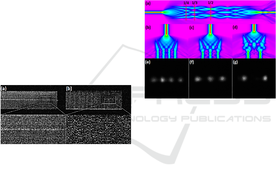
simulations were made with Rsoft (see figure 5 (a)
to (d)) using a 2D model and a 7x10
-3
refractive
index difference. In this work 1x4, 1x3 and 1x2
power splitters were investigated and the device
length was found to be, through simulation, roughly
690, 900 and 1350 µm, respectively. With the
fabrication parameters set above, several MMI
devices were fabricated using the three designs
specified in section 2. All these designs were tested
in an effort to improve the device symmetry and
decrease stresses originated by the fabrication
process. The first longitudinal design and the
transversal design showed very similar results in
terms of modal distribution (first longitudinal design
results are displayed in figure 5 (e) to (g)), while the
second longitudinal design did not show the
simulated behavior but rather random distributions.
It should be noted that the CCD from which the
modal distributions were measured does not have a
uniform sensitivity over its area, explaining why
unequal distribution is observed.
Figure 5: Figure showing the simulated behaviour and the
results obtained with the first longitudinal design for 50
µm width devices. First the 1:1 MMI behaviour is
simulated (a) and the 1:4 (b), 1:3 (c) and 1:2 (d)
simulations obtained for a length of 690, 900 and 1350 µm
respectively. From these simulated lengths the 1:4 (e), 1:3
(f) and 1:2 (g) behaviour was obtained experimentally.
These results can be explained by the microscope
images in figure 6. From the top view images, in
bright and dark field, it is possible to see that the
second longitudinal design is not as uniform as the
others. In the cross section view this becomes
obvious since the guiding region is much more
irregular. Apart from this, it is also interesting to
notice that the other two designs have problems. In
the first longitudinal design all MMI devices
fabricated had a crack in the corner of border B (last
waveguide to be written). This probably happens
due to stress accumulation on this corner, resulting
from the fact that waveguides were written from
border A to B. On the transversal design some
problems can also be identified by the dark field
image. This design was implemented since it avoids
the stress build-up but another problem arises due to
hardware communication times. At border B more
light is visible than at border A due to the laser being
Integrated Optical Devices - Fabrication of Multimode Interference Devices in Fused Silica by Femtosecond Laser Direct Writing
285

Figure 6: Top and cross section view microscopy images of the fabricated longitudinal and transversal MMI devices with a
waveguide separation of 0.5 µm.
ON while decelerating, which causes an increased
alteration of the local properties. Another interesting
fact is the stress concentration on the top region of
the MMI device, seen in the Differential Interference
Contrast (DIC) images, and also the higher light
scattering in this region for the longitudinal design
when compared with the transversal design.
4 CONCLUSIONS
The fabrication of multimode interference devices,
working at 1550 nm, was shown to be possible in
fused silica with the femtosecond laser direct writing
technique. Power splitting was achieved with
experimental results proving to be in good
agreement with BPM simulations. Splitters with a
splitting ratio of 1x4, 1x3 and 1x2 were fabricated
with a 50 µm width and a length of the multimode
section of 690, 900 and 1350 µm, respectively.
ACKNOWLEDGEMENTS
Vítor Amorim acknowledges the support of Calouste
Gulbenkian Foundation through the Stimulus to
Scientific Research Program (Grant no. 141773).
This work was also supported by Project
"NanoSTIMA: Macro-to-Nano Human Sensing:
Towards Integrated Multimodal Health Monitoring
and Analytics/NORTE-01-0145-FEDER-000016" is
financed by the North Portugal Regional Operational
Programme (NORTE 2020), under the PORTUGAL
2020 Partnership Agreement, and through the
European Regional Development Fund (ERDF).
REFERENCES
Hosseini, A, Kwong, D, Zhang, Y, Subbaraman, H, Xu, X
& Chen, R 2011, ‘1xN multimode interference beam
splitter design techniques for on-chip optical
interconnections’, IEEE Journal on Selected Topics in
Quantum Electronics, vol. 17, no. 3, pp. 510-515.
Soldano, L, Veerman, F & Smit, M 1992, “Planar
Monomode Optical Couplers Based on Multimode
Interference Effects”, Journal of Lightwave
Technology, vol. 10, no. 12, pp. 1843-1850.
Porque, J, Coudray, P, Charters, R, Kribich, K, Etienne, P
& Moreau, Y 2000, ‘WDM based on multimode
interferencecoupler built in an organic-inorganic
material’, Optics Communications, vol. 183, no. 1, pp.
PHOTOPTICS 2017 - 5th International Conference on Photonics, Optics and Laser Technology
286

45-49.
Al-hetar, A, Supa’at, A, Mohammad, A & Yulianti, I
2008, ‘Multimode interference photonic switches’
Optical Engineering, vol. 47, no. 11, pp. 112001.
Yu, F, Yamamoto, K, Piao, X & Yokoyama, S 2011,
‘Multimode interference waveguide switch of electro-
optic polymer with tapered access waveguides’,
Physics Procedia, vol. 14, pp. 25-28.
Eaton, S, Zhang, H & Herman, P 2005, ‘Heat
accumulation effects in femtosecond laser-written
waveguides with variable repetition rate’, Optics
Express, vol. 13, no. 12, pp. 4708-4716.
Zhang, H, Eaton, S & Herman, P 2007, ‘Single-step
writing of Bragg grating waveguides in fused silica
with an externally modulated femtosecond fiber laser’,
Optics Letters, vol. 32, no. 17, pp. 2559-2561.
Eaton, S, Chen, W & Zhang, L 2006, ‘Telecom-Band
Directional Coupler Written With Femtosecond Fiber
Laser’, Photonics Technology Letters, vol. 18, no. 20,
pp. 2174-2176.
Liu, J, Zhang, Z, Chang, S, Flueraru, C & Grover, C 2005,
‘Directly writing of 1-to-N optical waveguide power
splitters in fused silica glass using a femtosecond
laser’, Optics Communications, vol. 253, pp. 315-319.
Calmano, T, Siebenmorgen, J, Hellmig, O, Petermann, K
& Huber, G 2010, ‘Nd:YAG waveguide laser with 1.3
W output power, fabricated by direct femtosecond
laser writing’, Applied Physics B, vol. 100, no. 1, pp.
131-135.
Watanabe, W, Note, Y & Itoh, K 2005, ‘Fabrication of
multimode interference waveguides in glass by use of
a femtosecond laser’, Optics Letters, vol. 30, no. 21,
pp. 2888-2890.
Da-Yong, L, Yan, L, Yan-Ping, D, Heng-Chang, G, Hong,
Y & Qui-Huang, G 2008, ‘Transverse Writing of
Multimode Interference Waveguides inside Silica
Glass by Femtosecond Laser Pulses’, Chinese Physics
Letters, vol. 25, no. 7, pp. 2500-2503.
Integrated Optical Devices - Fabrication of Multimode Interference Devices in Fused Silica by Femtosecond Laser Direct Writing
287
