
Spectral Selective High Emissivity Pattern for Applications in near
Infrared
Enrique Carretero, Rafael Alonso and Cristina Pelayo
Department of Applied Physics, University of Zaragoza, C/Pedro Cerbuna, 12, 50009 Zaragoza, Spain
Keywords: Spectral Selective, Emissivity, Thin Films, Sputtering.
Abstract: In this work, we develop some high emissivity patterns for the near infrared range, between 1200 and
2500nm. These patterns were made by means of the magnetron sputtering technique, and they achieve their
functionality by using the optical interference phenomenon so that their superficial reflectance is
diminished. This is how we manage to produce surfaces that have a very low reflectance and high spectral
emissivity in the abovementioned range. Such patterns can be used for the calibration of temperature-
measuring systems based on photodiodes detecting near infrared radiation.
1 INTRODUCTION
It is well known that all bodies emit radiation, as the
black body theory describes. The total hemispherical
spectral emissive power or radiance of a surface
(DeWitt and Nutter, 1988; Howell et al., 2015),
namely, E
λ
(λ, T), is the power density distribution
emitted into the hemispherical solid per unit of
surface area whose dependence is provided by the
following equation:
2
5
2
,
1
hc kT
hc
ET
e
(1)
where T is the absolute temperature,
is the
wavelength of the radiation, h is the Planck constant,
c is the speed of light in vacuum and k is the
Boltzmann constant. But real bodies do not emit
radiation in the same way as a black body would do,
because they are not really “black”. The concept of
“emissivity” is introduced to take this into account.
The emissivity of an object is determined by its
absorption, so it can be measured with a
spectrophotometer, using the following expression:
1 RT
(2)
where ε(λ) is the spectral emissivity of the object,
R(λ) is its spectral reflectance and T(λ) is its spectral
transmittance. In this way, the total hemispherical
spectral emissive power or radiance of a real surface
is:
2
5
2
,
1
hc kT
hc
ET
e
(3)
Emissivity is very important for a lot of
applications, for instance, in the field of
concentrated solar power. The receiver tubes where
solar radiation must be concentrated on need to be
highly absorbent, that is, they need to have a high
emissivity in the spectral range where the sun emits
its maximum radiation (black body radiation at
5700K), between 300 and 2500nm (Setien-
Fernandez et al., 2013). At the same time, these
tubes must keep at a minimum the losses due to
emitted radiation when heated to 673K, so they must
have a low emissivity in the spectrum range of a
black body at 673K, between 2.5 and 30 μm. In
order to fulfil these requirements, selective coatings
are deposited by PVD (Physical Vapour Deposition)
techniques (Cao et al., 2015; Céspedes et al., 2014;
Hernandez-Pinilla et al., 2016; H.J.Gläser, 2000).
Nowadays, the improved performance and
lowered prices of InGaAs PIN photodiodes has
allowed its use for small signal detection in near
infrared for domestic appliances, temperature
measurement in cooking vessels from cooktops
being one example of this. This system is based on
the measurement of the black body radiation emitted
by a pot when cooking at temperatures between 100
and 200ºC (Imaz et al., 2014; Lasobras et al., 2014).
The photodiode is located inside the cooktop, under
the ceramic glass surface, so light detection must be
carried out in a wavelength range where the ceramic
glass is transparent. Such requirement rules out other
260
Carretero E., Alonso R. and Pelayo C.
Spectral Selective High Emissivity Pattern for Applications in near Infrared.
DOI: 10.5220/0006167102600264
In Proceedings of the 5th International Conference on Photonics, Optics and Laser Technology (PHOTOPTICS 2017), pages 260-264
ISBN: 978-989-758-223-3
Copyright
c
2017 by SCITEPRESS – Science and Technology Publications, Lda. All rights reserved

options measuring in wavelength ranges above 3μm,
although pots and pans in the abovementioned
cooking temperature range emit most of the
radiation above 3μm. InGaAs photodiodes detect
radiation between 600 and 2500nm. A surface
heated to 100ºC emits very little power in this
wavelength range, but this type of photodiodes is
sensitive enough to measure it.
One important issue with these detectors is its
calibration. They need to be calibrated with very low
emissive patterns and also with very high emissive
patterns. Low emissive patterns are very easy to
produce, because there is a great number of metals
which are low emissive in near infrared, as gold. On
the other hand, it’s easy to find a high emissive
surface with values around ε=0.90 in the detection
range of InGaAs PIN photodiodes, such as “burnt-
out” surfaces, but we have been able to produce a
pattern which has a higher emissivity (ε>0.97) than
traditional surfaces in this detection range. Such
patterns permit us to obtain a greater signal in the
temperature sensor of a cooktop.
Highly emissive patterns were produce by means
of the magnetron sputtering technique. These
patterns can be obtained by combining metallic and
dielectric layers (Sergeant et al., 2009). A coating
was deposited comprised of 4 layers, using both an
absorbent metallic material (Stainless Steel 316) and
a transparent dielectric material (SiAlN
x
) in a way
that the coating results opaque (T=0) and has a
minimal superficial reflectance between 1200 and
2500nm, using interferential coatings.
2 MATERIAL AND METHODS
Spectral Selective High Emissivity Patterns were
deposited in a semi-industrial high vacuum
magnetron sputtering system by the DC pulsed
technique using rectangular targets with dimensions
600x100mm and 12mm thick. Substrates were
ceramic glass pieces of 100x100mm and 4mm thick.
Ceramic glass has low thermal expansion coefficient
which makes it resistant to high temperatures
gradients without breaking. Substrates were cleaned
with a detergent solution (ACEDET 5509) and
finally rinsed with distilled water. A Stainless Steel
disc was also used to simulate a rough metallic
surface.
Thin films were grown with a base pressure of
2.0·10
-6
mbar and working pressure in the range of
10
-3
mbar. Ar and O
2
(both 99.99%) flows were
introduced into the process chamber and controlled
via mass flow controllers. The substrate was
maintained at room temperature during deposition.
Thin films of Stainless Steel (Sst) were deposited
from a Sst 316 target (99.99% pure). Applied power
was 2000W, equivalent to a power density of
3.33W/cm
2
. The Ar flow was fixed at 200sccm,
equivalent to a pressure of 1.5·10
-3
mbar in our
deposition system. Thin films of SiAlN
x
were
deposited by reactive sputtering from a Si-Al target
(90% Si and 10% Al, 99.99% pure). Applied power
was 2500W, equivalent to a power density of
4.17W/cm
2
. The Ar flow was fixed at 100sccm and
the N
2
flow at 100sccm.
Spectrophotometric measurements were
performed with a home-made spectrophotomer
(designed and built by some of the authors) in the
near-infrared region of the electromagnetic
spectrum, between 1100nm and 2500nm with 50nm
intervals, at an angle of incidence of 8º. The specular
reflectance of the patterns deposited over smooth
surfaces was measured without an integrating
sphere, because the low roughness of the substrate
minimizes the scattered component to negligible
values and because the specular measurements are
more precise. For patterns deposited over a rough
surface, reflectance measurements were carried out
through an integrating sphere. Finally, a
transmittance measurement was taken to verify the
low transmittance of the patterns.
3 RESULTS AND DISCUSSION
There are diverse types of InGaAs photodiodes
having different sensitive ranges. The most common
ones are those capable of detection radiation
between 600 and 1700nm, but there are extended
sensitivity models which can detect radiation
between 800 and 2600nm. On the other hand,
temperature sensors must be calibrated between 100
and 250ºC, and in this temperature range the black
body radiation below 1200nm is negligible. So the
objective of this work is to minimize reflectance in
the range between 1200 and 2500nm. For this
purpose, we designed an interference multilayer
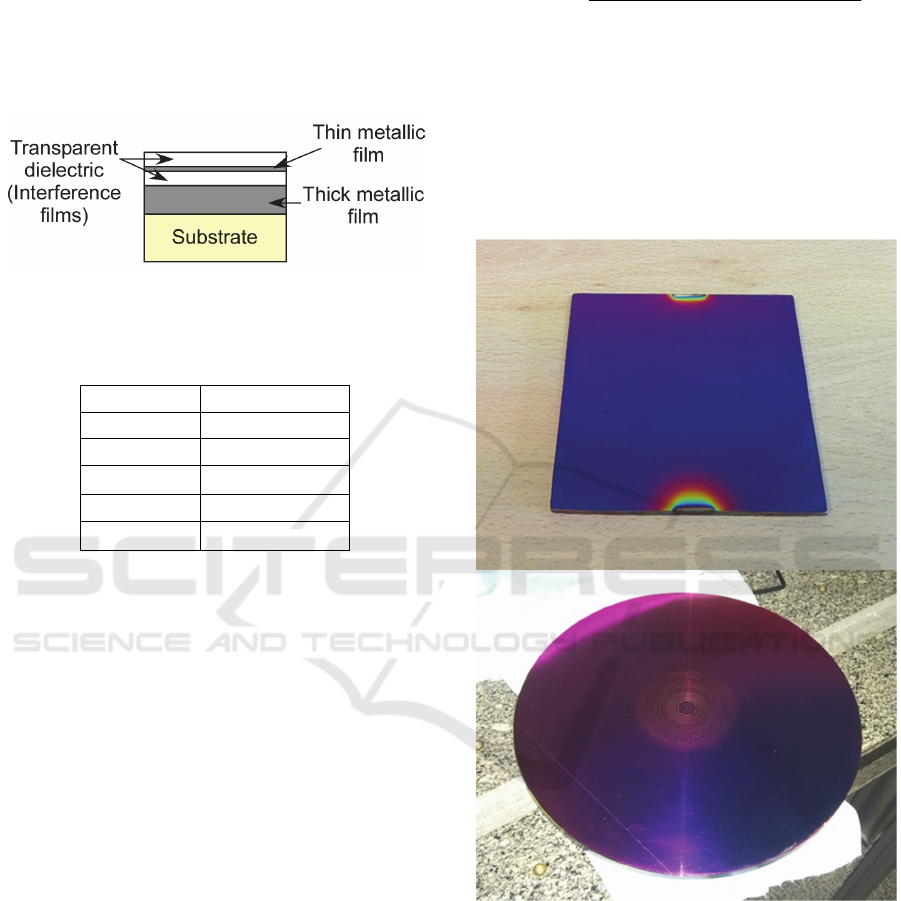
comprised of 4 layers, fig.1:
A first “thick” metallic layer (over 200nm)
directly deposited on the substrate. This layer has a
double functionality: for transparent substrates, this
layer has a high optical absorption, so the pattern
can be opaque (T=0), and furthermore, it will act as
a basic layer to calculate the interferential coating
which minimizes reflectance between 1200 and
2500nm.
The thicknesses of the three subsequent layers
must be adjusted very precisely, because they
Spectral Selective High Emissivity Pattern for Applications in near Infrared
261
determine the reflectance of the pattern. For this
purpose, the coating was simulated with the aid of
existing formalisms for the calculation of the optical
properties of interferential coatings (J. A.
Dobrowolski, 1995; Macleod, 2010; Thelen, 1989).
Values minimizing reflectance as required are
shown in table 1.
Figure 1: Multilayer structure of high emissivity patterns.
Table 1: Multilayer structure and layer thicknesses of
produced patterns.
Material Thickness (nm)
Substrate
Sst >200
SiAlN
x
186
Sst 13
SiAlN
x
204
Thus, we proceeded with the experimental
making of the patterns, both on ceramic glass and on
metallic discs, as depicted in Fig.2. So two patterns
were made: a specular pattern and a non-specular
one, the last one owing its feature to the roughness
of the substrate surface. These patterns visually
appear as purple coloured, because interferential
coatings usually produce striking colours. The fact
that they are (almost) black bodies in the 1200-
2500nm range is remarkable, considering this is not
true for the visible part of the spectrum, as they
indeed have a high reflectance at some particular
wavelengths.
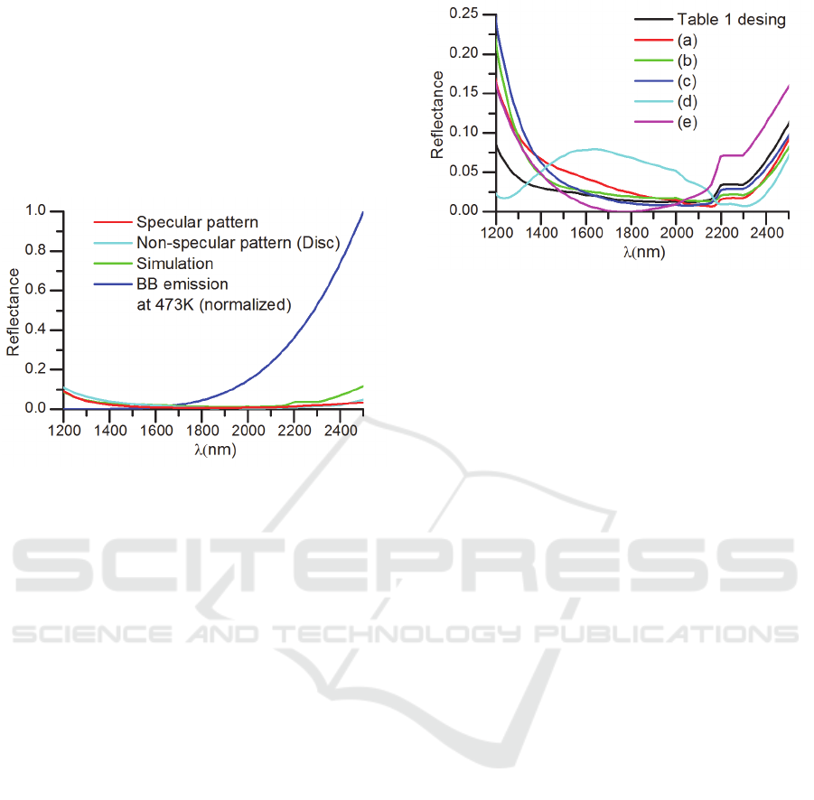
Figure 3 shows the reflectance curves of the two
produced patterns. In both cases we find similar
values of reflectance in spite of the differences over
surface texture of both substrates. Additionally,
measured values satisfactorily agree with simulated
values. On behalf of these results and knowing the
sensibility of the photodiodes provided by the
manufacturer, which in this particular case is
Teledyne Judson Technologies LLC, as we have
used models J22-18I-R01M and J2318I-R01M-2.6
(detecting respectively up to 1700 and 2600nm), we
can calculate the integrated apparent emissivity of
our patterns with this expression:
1700
0
1700
0
,1
()
,
SET Rd
T
SETd
(4)
Where S is the sensitivity of the J22-18I-R01M
photodiode, R is the spectral reflectance of the
pattern, ε is the integrated apparent emissivity at the
temperature T of the pattern as calculated for the
photodiode which detects up to 1700nm. This last
magnitude has a value of ε
1700
(473K)=0.987 for a
temperature of 473K.
Figure 2: Images of the produced patterns on ceramic
glass (top) and on a rough metallic disc (bottom).
We can repeat this procedure for the extended-
range photodiode that detects up to 2600nm,
modifying only the value of S
1700
(λ) for S
2600
(λ) in
expression (4), and we obtain an integrated apparent
emissivity of ε
2600
(473K)=0.976 Finally, we were
able to verify that our patterns produced the greatest
measured signals over all surfaces that were
measured with the temperature sensor (Imaz et al.,
2014; Lasobras et al., 2014).
PHOTOPTICS 2017 - 5th International Conference on Photonics, Optics and Laser Technology
262
One must keep in mind that the integrated
apparent emissivity is a magnitude taking into
account the spectral width between 1200 and
2600nm. Concerning spectral emissivity, values as
high as ε(1850nm)=0.994 were reached.
Nevertheless, if the final aim of the pattern was to
maximize emissivity at a particular wavelength
(instead of a wide range), it could be possible to
obtain values closer to 1.
Figure 3: Reflectance curves measured and simulated for
the highly emissive produced patterns, and normalized
black body emission at 473K.
One very significant issue is the tolerance in the
thickness of the deposited layers, because any
variation in these thicknesses can affect the
reflection spectrum of the pattern. Figure 4 shows
the changes in reflection spectra for coatings in
which some of its layers have a thickness deviated
from the values given in Table 1. One can appreciate
in this figure how an increment in the thickness of
the outer layer increases reflectance in the 1200-
1800nm range and decreases it in the 2100-2500nm
range. On the other hand, a 10% increment in both
dielectric layers shifts the low reflectance zone
towards higher wavelengths, whereas a 10%
increment in all the coating layers produces a slight
displacement and narrowing of the low reflectance
zone. If the thin metallic film has a 30% thinner
thickness, the wide part of the spectrum with low
reflectance disappears and two reflectance
minimums appear at 1250 and 2300nm. If that same
film has a 30% thicker thickness, the low reflectance
zone is narrowed but very low reflectance values can
be achieved at a specific wavelength (1780nm for
the studied case).
Figure 4: Simulated reflectance spectra for coatings with
different thicknesses: multilayer structure as described in
Table 1 (black line), (a) Outer transparent dielectric layer
with a 10% thicker thickness than in Table 1, (b) both
dielectric layers with a 10% thicker thickness, (c) All
layers with a 10% thicker thickness, (d) Thin metallic film
with a 30% thinner thickness, (e) Thin metallic film with a
30% thicker thickness.
So it can be concluded that layer thicknesses
must be adjusted with a tolerance lower than 10%
and preferably lower than 3%. Nevertheless, coating
adjustment is an iterative process where a coating is
deposited with thickness values near those exposed
in the table, then the reflectance of the coating is
measured and the experimentally obtained results
are adjusted by means of a simulation software in
such a way that we can know which thicknesses
must be modified for a better adjustment of optical
properties. In this way, these results can be
reproduced in other deposition systems, although
small further tuning of thicknesses might be
required.
It is remarkable that this kind of patterns can be
produced using different materials. Other dielectric
materials such as oxides and nitrides (SnO
2
,
Al
2
O
3
…) can be used, although they may require
thicknesses to be recalculated because of their
different index of refraction. SSt can also be
replaced by other metals commonly employed for
the fabrication of selective coatings in the solar
energy field, such as Mo, W…
4 CONCLUSIONS
Highly emissive patterns can be used to calibrate
temperature sensors based on infrared radiation
detection. We have made two highly emissive
patterns in the 1200-2500nm range, one of them
being specular and the other diffuse on a rough
Spectral Selective High Emissivity Pattern for Applications in near Infrared
263

surface, and both reaching values over 0.97.
Moreover, we have proven the feasibility of
reaching spectral emissivities over 0.99 at particular
wavelengths, by means of interferential multilayer
deposition. These patterns were used to calibrate a
temperature sensor. Finally, a good agreement
between simulated and measured values of
reflectance has been verified for these coatings.
ACKNOWLEDGEMENTS
We thank Carmen Cosculluela for her valuable help.
This work was partly supported by the Spanish
MINECO under grant RTC-2014-1847-6, in part by
the Diputación General de Aragón / Fondo Social
Europeo through the funding for the Photonics
Technologies Group (GTF), in part by the
Diputación General de Aragón under FPI
programme B143/12 and in part by the BSH Home
Appliances Group.
REFERENCES
Cao, F., Kraemer, D., Sun, T., Lan, Y., Chen, G., Ren, Z.,
2015. Enhanced Thermal Stability of W-Ni-Al2O3
Cermet-Based Spectrally Selective Solar Absorbers
with Tungsten Infrared Reflectors. Adv. Energy Mater.
5, 1401042. doi:10.1002/aenm.201401042.
Céspedes, E., Wirz, M., Sánchez-García, J.A., Alvarez-
Fraga, L., Escobar-Galindo, R., Prieto, C., 2014. Novel
Mo–Si3N4 based selective coating for high
temperature concentrating solar power applications.
Sol. Energy Mater. Sol. Cells 122, 217–225.
doi:10.1016/j.solmat.2013.12.005.
DeWitt, D.P., Nutter, G.D., 1988. Theory and Practice of
Radiation Thermometry. John Wiley & Sons.
Hernandez-Pinilla, D., Rodriguez-Palomo, A., Alvarez-
Fraga, L., Cespedes, E., Prieto, J.E., Munoz-Martin,
A., Prieto, C., 2016. MoSi2-Si3N4 absorber for high
temperature solar selective coating. Sol. Energy
Mater. Sol. Cells 152, 141–146.
doi:10.1016/j.solmat.2016.04.001.
H.J.Gläser, 2000. Large Area Coating. Von Ardenne
Anlagentechnik GmbH, Dresden.
Howell, J.R., Menguc, M.P., Siegel, R., 2015. Thermal
Radiation Heat Transfer, 6th Edition. CRC Press.
Imaz, E., Alonso, R., Heras, C., Salinas, I., Carretero, E.,
Carretero, C., 2014. Infrared thermometry system for
temperature measurement in induction heating
appliances. IEEE Trans. Ind. Electron. 61, 2622–2630.
doi:10.1109/TIE.2013.2281166.
J. A. Dobrowolski, 1995. Optical properties of films and
coatings., in: Handbook of Optics. McGraw-Hill.
Lasobras, J., Alonso, R., Carretero, C., Carretero, E.,
Imaz, E., 2014. Infrared sensor-based temperature
control for domestic induction cooktops. Sens. Switz.
14, 5278–5295. doi:10.3390/s140305278.
Macleod, H.A., 2010. Thin-Film Optical Filters, Fourth
Edition. CRC Press.
Sergeant, N.P., Pincon, O., Agrawal, M., Peumans, P.,
2009. Design of wide-angle solar-selective absorbers
using aperiodic metal-dielectric stacks. Opt. Express
17, 22800–22812.
Setien-Fernandez, I., Echaniz, T., Gonzalez-Fernandez, L.,
Perez-Saez, R.B., Cespedes, E., Sanchez-Garcia, J.A.,
Alvarez-Fraga, L., Escobar Galindo, R., Albella, J.M.,
Prieto, C., Tello, M.J., 2013. First spectral emissivity
study of a solar selective coating in the 150-600
degrees C temperature range. Sol. Energy Mater. Sol.
Cells 117, 390–395.
doi:10.1016/j.solmat.2013.07.002.
Thelen, A., 1989. Design of Optical Interference Coatings.
McGraw-Hill.
PHOTOPTICS 2017 - 5th International Conference on Photonics, Optics and Laser Technology
264
