
Low-loss 1310nm/1550nm Integrated Silicon Duplexer based on a
Directional Coupler
Daivid Fowler
1
, Bertrand Szelag
1
, Vincent Hugues
1
, Christian Sillans
2
,
Stéphane Bernabé
1
and Christophe Kopp
1
1
Univ. Grenoble Alpes, CEA, LETI, MINATEC campus, F38054 Grenoble, France
2
IFOTEC, ZAC de Champfeuillet, Route des Bois, 38500 Voiron, France
Keywords: Silicon Photonics, Photonic Integrated Circuits, Passive Components, Multiplexer, Duplexer.
Abstract: We describe the design, fabrication and measurement of an integrated silicon photonics O-band/C-band
duplexer. The duplexer is based on a directional coupler and is designed to be polarisation insensitive at
1550nm in order to be used in conjunction with a broadband integrated edge coupler. The measured insertion
losses are <1.3dB with a -1dB bandwidth of ~80nm.
1 INTRODUCTION
The increasing maturity of integrated silicon
photonics technology means that it is becoming
increasingly attractive to substitute traditional
discrete optical componentry with a low cost
integrated solution. Here, we report the design,
fabrication and measurement of a 1310/1550nm
duplexer for use in bi-directional high-bitrate single-
fiber systems, which is relevant for 1000BASE-BX10
and FTTH.
The use of integrated silicon photonics in this type
of application could lead to significant cost reductions
by eliminating many of the precise mechanical
operations involved in the assembly of discrete
optical components, leaving only the attachment of
the fiber to the integrated source-detector-duplexer.
This potentially decreases the module costs by a
significant margin.
Figure 1: Typical circuit schematic for a 1000BASE-BX10
type gigabit Ethernet module.
Figure 1 shows a schematic of the circuit
considered here. A modulated source laser operating
at 1310nm passes through a duplexer before leaving
downstream on a single mode fibre via a broadband
fibre coupler. Incoming, upstream data arrives in the
same fibre, using a modulated 1550nm signal. The
state of polarisation of the incoming light from the
network is intrinsically unknown and unstable. This
light will then be transferred into a combination of TE
and TM modes in the on-chip waveguide via the
broadband edge-type fibre coupler (Vivien et al,
2009). While integrated germanium photodiodes
(Cardenas et al, 2014) are largely insensitive to the
polarisation state in the incoming waveguide,
photonic circuit waveguides tend to be designed in
order to avoid unwanted crosstalk between
polarisation states, and therefore have unequal
refractive index values for TM and TE modes.
Therefore, care must be taken that the duplexer not
only splits/combines 1310/1550nm light, but also
exhibits low polarisation dependent loss for the
1550nm light.
2 DESIGN
Silicon photonics devices for multiplexing have been
widely developed to address single-band operation
(e.g. DWDM or CWDM) (Okamoto, 2014), however,
these solutions are not necessarily appropriate for
inter-band applications. Such duplexing devices have
been demonstrated on a silicon platform using
diffractive gratings (Roelkens, 2007), the multimode
interference effect (Hong and Lee 2007) and planar
reflective gratings (S. Bidnyk et al, 2007). Here we
Fowler D., Szelag B., Hugues V., Sillans C., Bernabe S. and Kopp C.
Low-loss 1310nm/1550nm Integrated Silicon Duplexer based on a Directional Coupler.
DOI: 10.5220/0006158000950098
In Proceedings of the 5th International Conference on Photonics, Optics and Laser Technology (PHOTOPTICS 2017), pages 95-98
ISBN: 978-989-758-223-3
Copyright
c
2017 by SCITEPRESS – Science and Technology Publications, Lda. All rights reserved
95
describe the use of a directional coupler to obtain very
low (<1dB) insertion losses.
Directional couplers are based on the transfer of
an optical field between two identical adjacent
waveguides via the coupling of evanescent modes.
They are often used in photonic circuits as a low-loss
component to separate the optical field in a single
waveguide into two waveguides with a pre-selected
intensity ratio. If a first waveguide carrying an optical
mode with a power, P
1
, runs parallel to a second
waveguide, the amount of transmitted power, P
2
, is
given by
⁄
, (1)
where L is the length of the parallel waveguides,
lambda is the operating wavelength and
is the
difference between the symmetric and antisymmetric
coupled modes, which is a function of wavelength,
waveguide geometry and the gap between the two
waveguides. Thus, the length of parallel waveguide
required in order to fully transfer the optical field
from one waveguide to another and back again, L
tot,
is
given by
⁄
.
(2)
With the use of a 2D mode solver (in this case RSOFT
FEMSIM), it is therefore possible to determine the
theoretically required coupling length in order to split
the 1310/1550nm wavelengths while implementing
polarisation insensitivity at 1550nm.
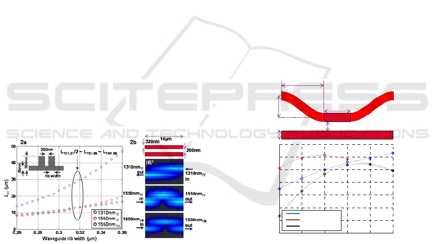
Figure 2a: L
tot
versus waveguide rib width. Inset: waveguide
geometry in coupling region. Figure 2b: Electrical field
intensity plots along the coupling region illustrating the
multiplexing mechanism.
Figure 2 shows L
tot,
as a function of waveguide rib
width for a waveguide spacing of 200nm for a
1.31µm TE mode (blue circles), a 1.55µm TE mode
(red circles) and 1.55µm TM mode (black circles).
The inset in the figure shows the waveguide geometry
used. We opted for a ‘rib’ type waveguide with a
continuous 65nm slab region for consistency with our
standard process, although other waveguide
geometries could offer valid starting points. For a
fixed gap between the waveguides of 200nm, the
values of L
tot
can be obtained as the rib width is
varied. In order to satisfy the function defined in
figure 1, we require
L
tot
(1.55
TE
) = L
tot
(1.55
TM
) = L
tot
(1.31
TE
)/2. (3)
When this condition is satisfied, the duplexing
functionality of the directional coupler is as illustrated
in the electric field intensity plots in figure 2b. This is
well approximated for a rib width of 315/320nm,
where L
tot
(1.55
TE
) = 13.0/13.5µm, L
tot
(1.55
TM
) =
13.0/13.3µm and L
tot
(1.31
TE
)/2 = 14.0/14.7µm.
While the above analysis provides a good starting
point for the directional coupler design, in reality, the
parallel waveguides must approach one other and
separate gradually, so as not to incur unwanted
bending losses. The actual design is shown in figure
3a. The waveguides are brought together using a sin-
function bend whose minimum bending radius is
11µm. Although the coupling strength between the
two waveguides decreases exponentially with the gap
between them, the power transfer which occurs in the
input and output bent waveguide sections is not
negligible and is most simply simulated using 3D-
FDTD (RSOFT FULLWAVE).
Figure 3a: Implemented directional coupler geometry
including input/output S-bends. 3D-FDTD simulated
insertion losses (data points in circles, the solid lines are a
guide for the eye).
Figure 3 shows the simulated insertion losses for the
1.31
TE,
1.55
TE
and the
1.55
TM
waveguide modes as a
function of the length of the straight coupling section.
In order to obtain less than 1dB insertion losses per
channel, the FDTD simulations, which included the
initial S-bends, revealed that a straight coupling
length of between 7 and 9 µm is required. This is
rather less than the value attained in the simple model
6.5 7 7.5 8 8.5 9
-1.4
-1.2
-1
-0.8
-0.6
-0.4
-0.2
0
Insertion losses (dB)
320nm
200nm
7µm
7,5µm
0,5µm
Straight coupling section length (µm)
1310nm
TE
cross
1550nm
TE
bar
1550nm
TM
bar
3a
3b
PHOTOPTICS 2017 - 5th International Conference on Photonics, Optics and Laser Technology
96

described above, which is due to the significant
coupling which takes place in the input/output bent
waveguide sections.
3 FABRICATION AND TEST
Test structures were fabricated at CEA-LETI on
200mm wafers with a SOI/BOX thickness of
310/800nm. Waveguides were defined using 193nm-
DUV lithography and a dry etching process (B.
Szelag, 2016).
Figure 4: Measured insertion losses of best performing
fabricated design variant. Solid lines are fit lines to the data
(points), dashed lines are 3D-FDTD simulations of the
nominal structure.
Test structures with a range of nominal waveguide
widths and coupling section lengths were fabricated.
Each variant was triplicated and connected to vertical
fibre grating couplers designed to couple
1.31µmTE/1.55µmTE/1.55µmTM light into the
waveguides. In order to evaluate the insertion losses
for each channel, a reference waveguide was
measured with each type of fibre coupler. The ‘cross’
transmission (corresponding to light crossing from
one guide to another) and the ‘bar’ transmission
(corresponding to light propagation along the same
waveguide) of each variant was then measured for
each channel. The directional coupler transmission
spectra were then obtained by subtracting the
corresponding fibre coupler spectra from the
directional coupler transmission data.
The transmission spectra of the best performing
variant (rib width = 320nm, gap = 200nm, coupling
section length = 7µm) are shown in figure 4. The data
points are shown as well as polynomial fits (solid
lines). The high noise level of the data can be
attributed to the summing of the noise in the
transmission spectra and the reference spectra. The
measured insertion losses for the
1.31µmTE/1.55µmTE/1.55µmTM channels were -
0.6/-0.55/-1.2dB. The measured -1dB bandwidth is in
the region of 80nm. The use narrowband fibre grating
couplers prevented crosstalk measurements, although
FDTD simulations show values in the -10 to -15dB
range.
For comparison, the 3D-FDTD simulated
transmission spectra for this nominal structure are
also shown as dashed lines on figure 4. The observed
discrepancy as well as the fact that the best
performing variant (rib width = 320nm, L = 7µm) was
not exactly that identified via FDTD simulation may
be firstly attributed to the unsimulated optical
coupling in the waveguide routing required to access
the test structure and secondly, to departures from the
nominal waveguide geometry in the processed
devices.
4 CONCLUSIONS AND
PERSPECTIVES
We have designed, fabricated and measured an
integrated silicon low loss O-band/C-band duplexer
with polarisation insensitivity at 1550nm. The device
shows low measured losses (<1.3dB) at each design
wavelength. Further design refinements will likely
reduce insertion losses significantly below 1dB,
which compares favourably with conventional,
discrete optical componentry. Based on this positive
result, we are now fabricating a complete circuit,
including integrated laser, photodiode and broadband
edge coupler to demonstrate the potential of
integrated silicon photonics for this application.
REFERENCES
L. Vivien, J. Osmond, Jean-Marc Fédéli, Delphine Marris-
Morini, Paul Crozat, Jean-François Damlencourt, Eric
Cassan, Y. Lecunff, and Suzanne Laval, "42 GHz p.i.n
Germanium photodetector integrated in a silicon-on-
insulator waveguide," Opt. Express 17, 6252-6257
(2009).
J. Cardenas, C. B. Poitras, K. Luke, L Luo, P.A. Morton,
and M. Lipson. 2014. High Coupling Efficiency Etched
Facet Tapers in Silicon Waveguides, IEEE Photonics
Technology Letters, Vol. 26, No. 23.
K. Okamoto, 2014. Wavelength-Division Multiplexing
Devices in Thin SOI: Advances and Prospects, IEEE
Journal of Selected Topics in Quantum Electronics,
Vol. 20, NO. 4.
G. Roelkens, D. Van Thourhout, and R. Baets. 2007.
Silicon-on-insulator ultra-compact duplexer based on a
Low-loss 1310nm/1550nm Integrated Silicon Duplexer based on a Directional Coupler
97

diffractive grating structure. Opt. Express 15, 10091-
10096.
J.K. Hong and S.S. Lee. 2007. 1 x 2 Wavelength
Multiplexer With High Transmittances Using
Extraneous Self-Imaging Phenomenon," J. Lightwave
Technol. 25, 1264-1268.
S. Bidnyk, M. Pearson, A. Balakrishnan, M. Gao, D. Feng,
H. Liang, W. Qian, C. Kung, J. Fong, P. Zhou, J. Yin,
and M. Asghari, 2007. Silicon-on-Insulator Platform
for Building Fiber-to-the-Home Transceivers, in
Optical Fiber Communication Conference and
Exposition and The National Fiber Optic Engineers
Conference, OSA Technical Digest Series (CD)
(Optical Society of America), paper OTuM4.
B. Szelag ; B. Blampey ; T. Ferrotti ; V. Reboud ; K.
Hassan, et al. Multiple wavelength silicon photonic 200
mm R+D platform for 25Gb/s and above applications,
2016. Proc. SPIE 9891, Silicon Photonics and Photonic
Integrated Circuits V, 98911C (May 13, 2016);
doi:10.1117/12.2228744.
PHOTOPTICS 2017 - 5th International Conference on Photonics, Optics and Laser Technology
98
