
Semiconductor Laser Beam Quality Metrics for Free-Space Optical
Communications
James Beil
1
, Rebecca Swertfeger
1
, Stephen Misak
1
, Zihe Gao
2
, Kent D. Choquette
2
and Paul O. Leisher
1
1
Rose-Hulman Institute of Technology, 5500 Wabash Avenue, Terre Haute, IN, U.S.A.
2
University of Illinois Urbana-Champaign, Kirby Avenue, Champaign, IL, U.S.A.
Keywords: Beam Quality, Beam Propagation Factor, Beam Parameter Product, Diffraction-Limited, Gaussian, near-
Field, Far-Field, Beam Waist, Divergence Angle, Free-Space Optical Communications, Semiconductor Laser,
Diode Laser, Beam Metrics.
Abstract: The beam propagation factor, M
2
, exists as one of very few measures of a laser’s performance, when really a
more detailed analysis of the application and laser are necessary for judgement in most cases. In free-space
optical communications, a crucial figure of merit is the proportion of diffraction-limited power in the far-
field. A calculated structure has been made with a higher proportion of diffraction-limited power in the far-
field than another calculated structure with a much better M
2
. This calculated structure has an M
2
of 19, with
89% of its power within the diffraction limit in the far-field, compared to another calculated structure with
M
2
of 1.7 that has 86% of its power within the diffraction limit in the far-field.
1 INTRODUCTION
The beam propagation factor M
2
, often erroneously
called the “beam quality,” is a comparison of the
near- and far-field second moment widths of a given
beam to a fundamental Gaussian beam of the same
wavelength. A fundamental Gaussian beam is ideal,
meaning it can be focused down to a waist of minimal
size—subject to a certain numerical aperture—or
collimated such that its divergence angle is minimal,
and its M
2
is 1 (Saleh and Teich, 2007). Another way
of stating this is by calling the beam diffraction-
limited. M
2
is given as:
ω
(1)
Where ω
0
is the beam waist radius, θ
0
is the
divergence half-angle, and λ is the operating
wavelength (Saleh and Teich, 2007).
Since the operating wavelength is usually known or
easily measured, the beam waist and divergence angle
are the only two remaining beam metrics needed to
know M
2
. They are not as easy to measure and
calculate though, and as such, ISO has created
standard 11146 to specify procedures to do so.
Specifically, ISO mandates usage of the second
moment width of the near- and far-field intensity
distributions to determine beam waist and divergence
angle, respectively (1995).
Given the nature of the second moment, it is possible,
in theory, to use this definition of beam
waist/divergence angle in a way that brings light to
the faults of using M
2
as beam quality. For example,
begin with an intensity distribution of a fundamental
Gaussian beam. By placing a small amount of energy
very far from the central lobe of the distribution, the
second moment width could be made infinitely large,
even though a great proportion of the energy still lies
within the diffraction limit. This would, in turn, cause
M
2
to be large, even though the beam behaves very
similarly to a fundamental Gaussian beam.
This paper demonstrates that a structure with an M
2
much greater than 1 can be engineered such that most
of the power in the far-field lies within the diffraction
limit—as desired for free-space optical
communications. The significance of such a finding
is that larger semiconductor laser structures capable
of greater efficiency and higher power could be used
for free-space optical communications without
concerns about multimode activity. Additionally, M
2
196
Beil J., Swertfeger R., Misak S., Gao Z., Choquette K. and Leisher P.
Semiconductor Laser Beam Quality Metrics for Free-Space Optical Communications.
DOI: 10.5220/0006122601960201
In Proceedings of the 5th International Conference on Photonics, Optics and Laser Technology (PHOTOPTICS 2017), pages 196-201
ISBN: 978-989-758-223-3
Copyright
c
2017 by SCITEPRESS – Science and Technology Publications, Lda. All rights reserved
is an insufficient measure of beam quality for free-
space optical communications, and a different metric,
such as power in the bucket, would serve better.
2 CALCULATING A MODE
PROFILE AND A REFERENCE
GAUSSIAN PROFILE
The process of engineering a structure to meet the
design intents begins with a basic refractive index
profile: a centered region of higher refractive index,
as illustrated in figure 1.
Figure 1: A basic refractive index structure and its first
order mode profile. Note that many higher order modes are
also supported by this structure.
This profile results in a simple, somewhat Gaussian,
first order mode profile. The desired mode profile
contains some of its energy far from the center,
however, so this basic design is not sufficient on its
own. For high power applications, it is desirable to
have heat spread over a large physical area. Scaling
the first order mode size is not useful because the
index contrast required to do so is far too small for
real-world use—both due to manufacturing
limitations and sensitivity to thermal effects.
From the basic structure, one can observe that the
mode profile has a peak centered about the region of
higher refractive index. The desired profile features
additional peaks in the mode before and after the
central lobe, therefore the next evolution in the index
profile should be adding high index material before
and after the central lobe. Some additional factors to
consider are the thickness of each high-index material
layer and the magnitude of the index contrast between
the base material and the lobes of higher index. As a
demonstration of these effects, the structure observed
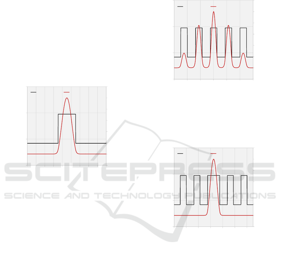
in figure 2 is first used as a reference.
Figure 2: A structure useful for demonstrating the effects of
changes to the index profile.
The central lobe of high-index material is then made
twice as wide, and the effects are observed in figure
3.
Figure 3: The same structure from Fig. 2, but with a wider
central region.
As demonstrated in figure 3, a thicker high-index
material pulls the first order mode into the lobe.
Again using the structure in figure 2 as a reference,
the refractive index contrast between the central lobe
and the base material is increased, and the effects are
observed in figure 4.
-0.2
0.0
0.2
0.4
0.6
0.8
1.0
1.2
3.367
3.368
3.369
3.370
0 102030405060708090
Modal Intensity (arb. units)
Index of Refraction
Position (um)
Index Profile First Order Mode
-0.2
0.0
0.2
0.4
0.6
0.8
1.0
1.2
3.367
3.368
3.369
3.370
0 20 40 60 80 100 120
Modal Intensity (arb. units)
Index of Refraction
Position (um)
Index Profile First Order Mode
-0.2
0.0
0.2
0.4
0.6
0.8
1.0
1.2
3.367
3.368
3.369
3.370
0 20406080100120
Modal Intensity (arb. units)
Index of Refraction
Position (um)
Index Profile First Order Mode
Semiconductor Laser Beam Quality Metrics for Free-Space Optical Communications
197
Figure 4: The same structure from Fig. 2, but with a greater
index contrast between the central region and the base
material.
A greater index contrast also pulls the first order
mode into the lobe. These two relations are a
consequence of solving the Helmholtz wave
equation:
Where U is the complex field and k is the wave
number (Goodman, 2005). The wave number k
depends on the refractive index. As such, the
normalized first order solution to the wave equation
is guided to the region of highest average refractive
index. The two methods demonstrated both direct that
region towards the center of the structure.
The first order mode is generally a good indication of
the behavior of the structure, however, one must still
take into account higher order modes, if any are
present in the laser, which adds additional levels of
complexity. As such, the process of engineering the
desired structure is an iterative one, requiring analysis
after each iteration.
Once an index profile is created, analysis can begin.
The modes—and therefore the near-field intensity
distribution—are calculated using a Ritz iterative
eigenmode solve of the Helmholtz wave equation
given in equation 2. The near-field intensity is given
by the absolute square of the complex field.
The far-field intensity distribution as a function of
angle is found via the absolute square of the Fourier
transform of the field near the aperture (Goodman,
2005). From this point forward, the profiles referred
to in the near- and far-field are the intensity
distributions.
It is worth note that even structures with exotic near-
field distributions have far-field distributions that
look mostly Gaussian in nature. For example, the
near- and far-field profiles for the structure from
figure 2 are displayed in figure 5. This is promising
evidence in support of the hypothesis that a structure
with poor M
2
can still have a large proportion of its
power within the diffraction limit in the far-field.
After engineering a structure to test, it is necessary to
create a reference Gaussian beam for that structure.
This is done using software to find the optimal
Gaussian for the near-field profile, based on the
overlap. Begin with the basic form of a Gaussian
function. Match the peak and mean to the peak and
centroid of the near-field profile, then iteratively vary
the width to find the best profile using the overlap
with the near-field profile as a figure of merit. The
result with the most overlap is the reference Gaussian
profile.
Figure 5: The near-field (left) and far-field (right) intensity profiles for the structure in Fig. 2.
-0.2
0.0
0.2
0.4
0.6
0.8
1.0
1.2
3.360
3.370
3.380
3.390
3.400
3.410
0 20406080100120
Modal Intensity (arb. units)
Index of Refraction
Position (um)
Index Profile First Order Mode
0.0
0.2
0.4
0.6
0.8
1.0
1.2
0 20406080100120
Near-Field Intensity (arb. units)
Position (um)
0.0
0.2
0.4
0.6
0.8
1.0
1.2
-10 -5 0 5 10
Far-Field Intesity (arb. units)
Angle (deg)
0
(2)
PHOTOPTICS 2017 - 5th International Conference on Photonics, Optics and Laser Technology
198
In order to obtain a reference for the diffraction limit
in the far-field, the Fourier Transform is used to
propagate the reference Gaussian profile to the far-
field. Important to note is the inverse nature of the
Fourier Transform, which means that a broad near-
field intensity profile will result in a narrow far-field
intensity profile, and vice-versa. Figure 5 is an
excellent example of this. The near-field profile is
relatively wide, and the far-field profile is in turn
quite narrow.
Provided a structure and its corresponding reference
Gaussian profile, calculations can be performed to
solve for M
2
and the proportion of diffraction-limited
power in the far-field. Firstly, the beam parameter
product (BPP) must be found for the reference
Gaussian profiles, and the engineered structure. The
BPP is simply defined as:
(3)
Where ω
0
is the beam waist in the near-field, and θ
0
is the divergence angle in the far-field. Beam waist
and divergence angle are found from the second
moment width of the near- and far-field profiles,
respectively, as per ISO standard 11146 (1995).
Since the M
2
of a fundamental Gaussian beam is
known to be 1, the M
2
of the engineered structure can
be found by dividing the BPP of the structure by the
BPP of the reference Gaussian profile, as their
operating wavelengths are assumed to be equal. The
diffraction-limited power in the far-field (or near-
field, if needed) may be calculated now using the
engineered profiles and the reference profiles. A
range for the diffraction-limited region must be
specified. One way of doing so is using the far-field
divergence angle (which was obtained earlier using
the second moment method) as follows:
(4)
Where θ
0
is the far-field divergence angle of the
reference Gaussian, and F(θ) is the far-field intensity
profile of the engineered structure, as a function of
angle.
3 RESULTS
There are four possible outcomes for a given
structure: M
2
can be relatively high or relatively low
(close to 1), and each of those cases can have a high
or low proportion of diffraction-limited power in the
far-field. The expected outcomes are those in line
with the current assumptions about M
2
. A small M
2
will have most of its power within the diffraction limit
because it is similar to a fundamental Gaussian beam,
and a large M
2
will have most of its power outside the
diffraction limit because it is dissimilar to a
fundamental Gaussian beam.
The significant outcome, the focus of this paper, is
that a structure with large M
2
can be engineered to
contain most of its power within the diffraction limit.
The other possible outcome—in which a structure
with small M
2
would have most of its power outside
the diffraction limit—falls outside the scope of this
paper.
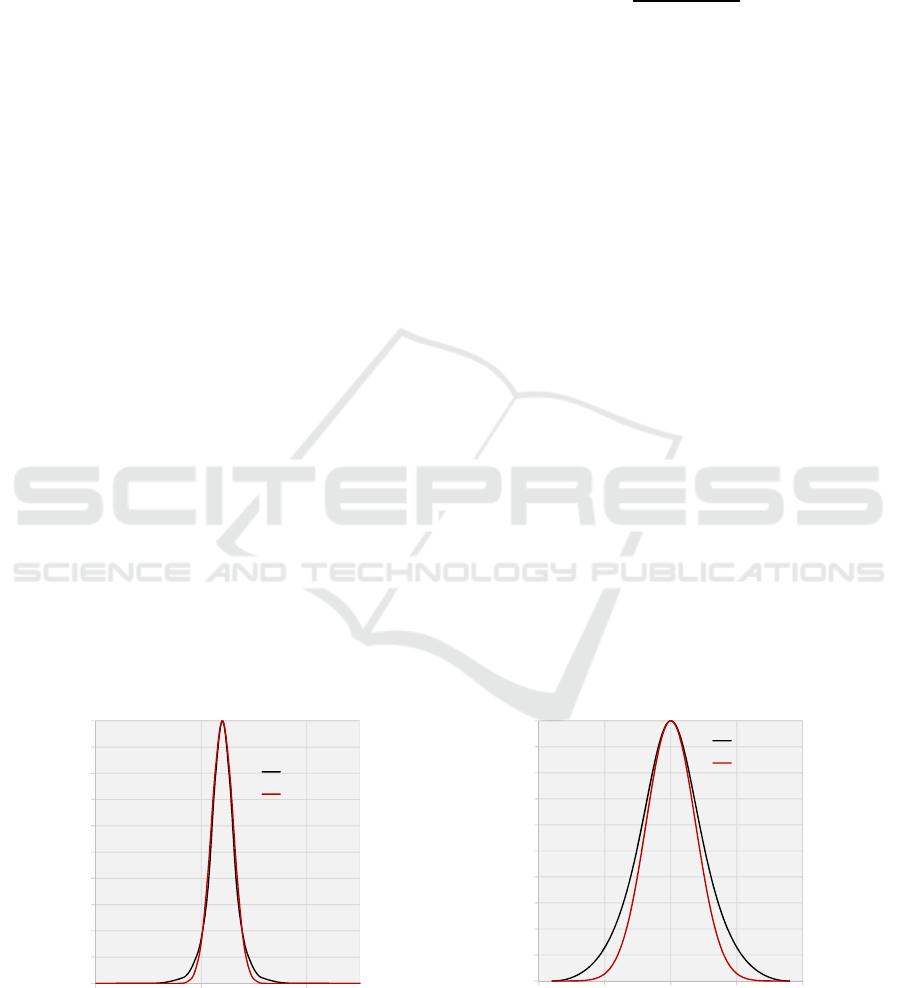
Figure 6: Near-field (left) and far-field (right) intensity distributions for an engineered structure with M
2
of 1.7 and 86 percent
of its power in the far-field within the diffraction limit.
0.0
0.1
0.2
0.3
0.4
0.5
0.6
0.7
0.8
0.9
1.0
567
Near-Field Intensity (arb. units)
Position
(
um
)
M²=1.7
M²=1
0.0
0.1
0.2
0.3
0.4
0.5
0.6
0.7
0.8
0.9
1.0
-100 -50 0 50 100
Far-Field Intensity (arb. units)
Angle (deg)
M²=1.7
M²=1
Semiconductor Laser Beam Quality Metrics for Free-Space Optical Communications
199
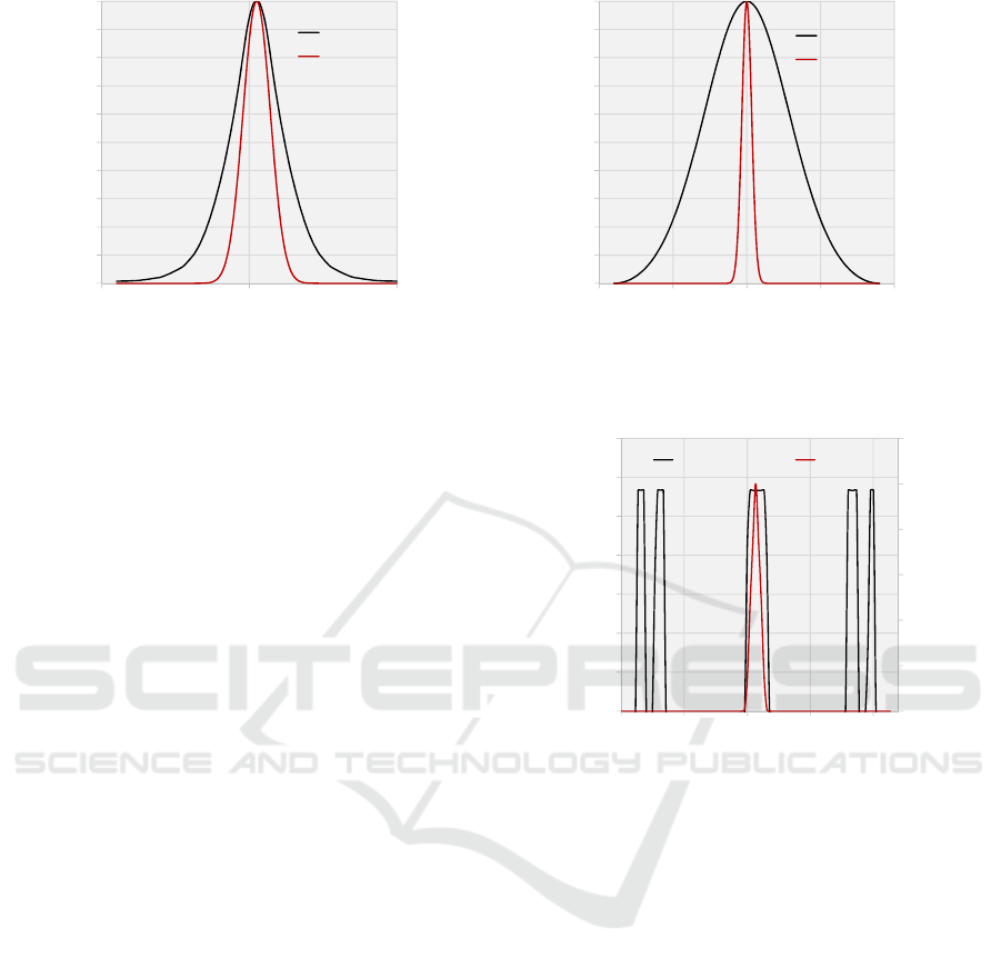
Figure 7: Near-field (left) and far-field (right) intensity distributions of an engineered structure operating with M
2
of 10 and
only 20% of its power in the far-field within the diffraction limit.
Figure 6 illustrates the first expected outcome; a small
M
2
resulting in most of its power within the
diffraction limit in the far-field—in this case 86
percent of the power within the diffraction limit for
an M
2
of 1.7. The reference Gaussian is also included
for visual comparison. As expected, the shape of the
near- and far-field profiles are quite similar to the
reference Gaussian hence the small M
2
. M
2
can be
visualized in these plots as the product of the
deviation of the black curve from the red curve in the
near- and far-field, as this is the visual manifestation
of the beam parameter product.
Figure 7 illustrates the second expected outcome; a
large M
2
resulting in most of the power outside the
diffraction limit—in this case only 20 percent of the
power in the far-field is within the diffraction limit,
and M
2
is 10. Although the shape of the near-field
profile looks very similar to the reference Gaussian,
the inverse nature of the Fourier transform exhibits
itself very strongly as the far-field profile for the
engineered structure is extremely broad compared to
the rather narrow reference Gaussian profile. Using
the beam parameter product definition from equation
(3), fixing wavelength to be the same, and assuming
that the beam waist are roughly the same, one can
conclude that the far-field divergence angle is about
10 times that of the reference Gaussian, hence the vast
difference in the size of the curves in the far-field
(Siegman, 1998).
Figure 8: The index profile and first order mode of the
engineered structure that supports the original hypothesis.
Figure 8 is the engineered structure that validates the
original hypothesis. Its near- and far-field intensity
distributions are shown in figure 9. It has an M
2
of 19
and contains 89 percent of its power in the far-field
within the diffraction limit—more than even the M
2
-
1.7 structure in figure 6. The structure was created by
cleverly manipulating the two lobes visible in the
near-field such that they are very far from the central
lobe relative to the width of the lobes. This makes the
beam waist, as defined by the ISO standard second
moment method, very large. This accomplishes two
things. Firstly, the far-field profile is narrow—much
narrower than that of an M
2
-19 beam would normally
be—thanks to the inverse nature of the Fourier
transform. Secondly, M
2
is large as a result of the
beam parameter product comparison with the
reference Gaussian.
0.0
0.1
0.2
0.3
0.4
0.5
0.6
0.7
0.8
0.9
1.0
012
Near-Field Intensity (arb. units)
Position
(
um
)
M²=10
M²=1
0.0
0.1
0.2
0.3
0.4
0.5
0.6
0.7
0.8
0.9
1.0
-100 -50 0 50 100
Far-Field Intensity (arb. units)
A
n
g
le
(
de
g)
M²=10
M²=1
0.0
0.2
0.4
0.6
0.8
1.0
1.2
3.358
3.360
3.362
3.364
3.366
3.368
3.370
3.372
0 50 100 150 200
Modal Intensity (arb. units)
Index of Refraction
Position (um)
Index Profile Mode 0
PHOTOPTICS 2017 - 5th International Conference on Photonics, Optics and Laser Technology
200
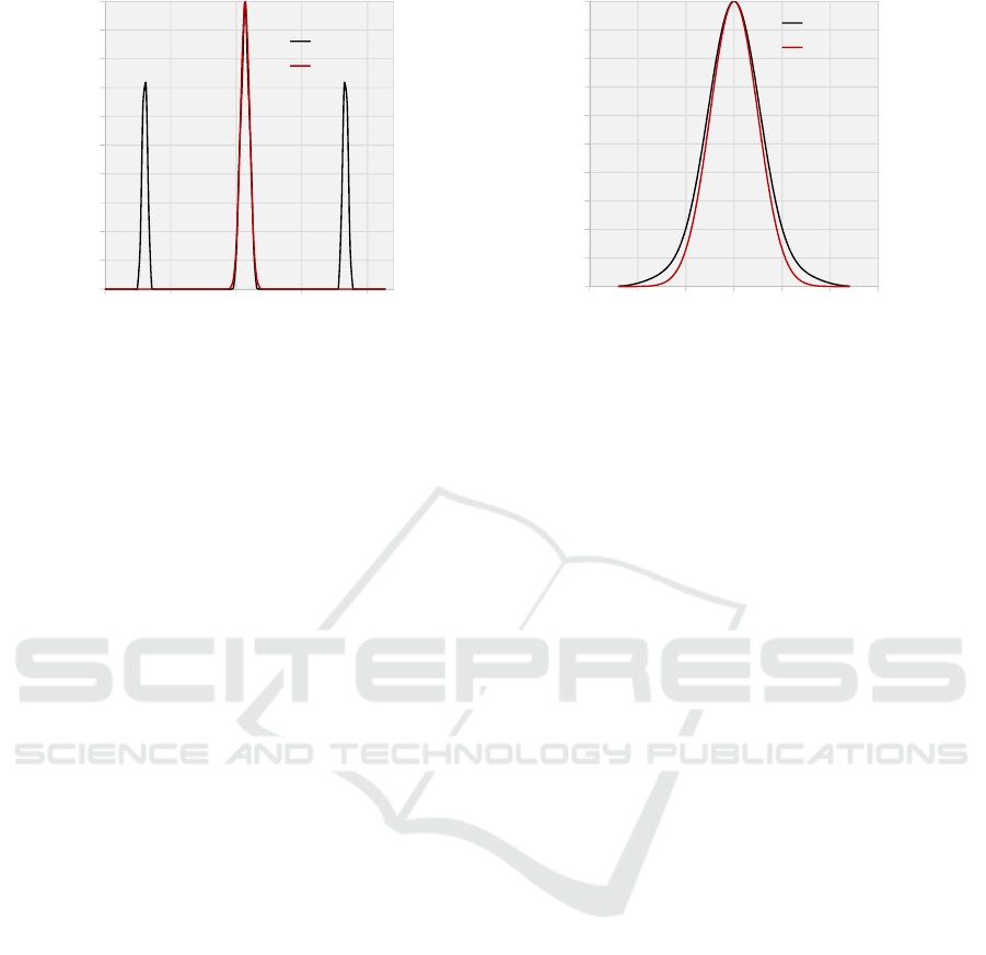
Figure 9: Near-field (left) and far-field (right) intensity distributions of an engineered structure operating with M
2
of 19 and
89% of its power in the far-field within the diffraction limit.
4 CONCLUSIONS
In conclusion, this paper demonstrates that a structure
with large M
2
can be engineered such that most of its
power lie within the diffraction limit is true. As a
result, M
2
is not an appropriate measure of beam
quality within the scope of free-space optical
communications. The significance of such a structure
is that a larger stripe width could be used in
semiconductor lasers without fear of multimode
activity, since diffraction-limited power is still large
relative to the total power available. This could allow
greater efficiency at higher power, as the trend
observed by Crump et al verifies (2009). The
engineered structure exhibited a greater proportion of
diffraction-limited power than another structure with
an M
2
ten times smaller. Perhaps the metric of beam
quality for semiconductor lasers needs rethinking,
especially in applications such as free-space optical
communications.
REFERENCES
Crump, P., Blume, G., Paschke, K., Staske, R., Pietrzak, A.,
Zeimer, U., Einfeldt, S., Ginolas, A., Bugge, F.,
Hausler, K., Ressel, P. Wenzel, H., and Erbert, G.,
2009. 20W continuous wave reliable operation of
980nm broad-area single emitter diode lasers with an
aperture of 96μm. Proc. SPIE 7198, High-Power Diode
Laser Technology and Applications VII, 719804.
doi:10.1117/12.807263
Goodman, J., 2005. Introduction to Fourier Optics. Roberts
& Company. 3
rd
edition.
ISO/TC 172, 1995. Terminology and test methods for
lasers.
Saleh, B. and Teich, M., 2007. Fundamental of Photonics.
John Wiley & Sons. 2
nd
edition.
Siegmann, A., 1998. How to (Maybe) Measure Laser Beam
Quality. OSA TOPS.
0.0
0.1
0.2
0.3
0.4
0.5
0.6
0.7
0.8
0.9
1.0
0 50 100 150 200
Near-Field Intensity (arb units)
Position
(
um
)
M²=19
M²=1
0.0
0.1
0.2
0.3
0.4
0.5
0.6
0.7
0.8
0.9
1.0
-15 -10 -5 0 5 10 15
Far-Field Intensity (arb. units)
Angle (deg)
M²=19
M²=1
Semiconductor Laser Beam Quality Metrics for Free-Space Optical Communications
201
