An Impedance Spectroscopy ASIC for Low-Frequency Characterization
of Biological Samples
Juan J. Montero-Rodr´ıguez
1,2
, Edgar Eduardo Salazar-Fl´orez
1
, Paola Vega-Castillo
1,2
,
Jakob M. Tomasik
∗
, Wjatscheslaw Galjan
∗
, Kristian M. Hafkemeyer
∗
and Wolfgang Krautschneider
1
1
Institute of Nano and Medical Electronics, Hamburg University of Technology, Hamburg, Germany
2
Escuela de Ingenier´ıa Electr´onica, Instituto Tecnol´ogico de Costa Rica, Cartago, Costa Rica
Keywords:
ASIC, Cell Concentration, Impedance Spectroscopy, Porcine Chondrocytes, Yeast.
Abstract:
This paper describes the design and testing of an ASIC for impedance spectroscopy of biological samples at
frequencies up to 40 kHz. The circuit is designed in the 350 nm AMS H35B4 technology and enables the
measurement of impedances in the range of 10 kΩ up to 28 MΩ. The design features a digital oscillator and
a current-to-voltage converter. The ASIC is used to monitor the growth of yeast cell cultures and porcine
chondrocytes, in real-time, using a standard 384-well plate and copper electrodes.
1 INTRODUCTION
Impedance Spectroscopy is a technique that can be
used to monitor different biomedical parameters, such
as glucose concentration (Hossain and Dhar, 2013),
blood lactate concentration (Alvarenga and Souza,
2007), and cell growth (Giaever and Keese, 1984).
Electrical measurements of the cell growth avoid
the use of toxic markers that may degrade the samples
(Giaever and Keese, 1986). If the applied voltages
are small, there is no cell stress and the cells do not
lose vitality. Also, the measurements can be easily
automatized, enabling real-time measurement of the
cell growth without damaging the cells.
This paper describes the implementation of an
Application Specific Integrated Circuit (ASIC) for
impedance spectroscopy of biological samples at
frequencies up to 40 kHz, for samples in the range
from 10 kΩ up to 28 MΩ. The chip was designed in
the AMS H35B4 technology of 350 nm.
This integrated circuit is used to measure
the impedance of samples by the Auto-balancing
Bridge Method (ABBM) described in the Impedance
Measurement Handbook (Keysight, 2015). The chip
allows the use of short wiring between the circuit
and the measurement chambers by placing the chip
directly on the back of commercial well plates.
∗
He was with the Institute of Nano and Medical
Electronics of Hamburg University of Technology at the
time the design of the ASIC was performed.
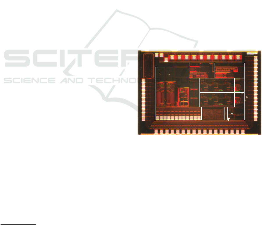
The top view of the ASIC is shown in Figure 1.
ADCADC
LPF
LPF
I2VOSC
SR32
Miller-C2OTA
CAP_array
Figure 1: Top layout of the ASIC.
In this paper the circuit is used to monitor
the growth of yeast cell cultures and porcine
chondrocytes in different experimental conditions,
such as the inclusion of sugar in the culture medium.
The structure of this paper is as follows. The
chip architecture and a detailed explanation of the
design is described in section 2. The impedance
computation with LabVIEW is described in section
3. The measurement setup is shown in section 4. The
experimental results from yeast cell measurements
are presented in section 5, and experiments with
porcine chondrocytes are described in section 6.
222
Montero-Rodríguez, J., Salazar-Flórez, E., Vega-Castillo, P., Tomasik, J., Galjan, W., Hafkemeyer, K. and Krautschneider, W.
An Impedance Spectroscopy ASIC for Low-Frequency Characterization of Biological Samples.
DOI: 10.5220/0005772202220228
In Proceedings of the 9th International Joint Conference on Biomedical Engineering Systems and Technologies (BIOSTEC 2016) - Volume 1: BIODEVICES, pages 222-228
ISBN: 978-989-758-170-0
Copyright
c
2016 by SCITEPRESS – Science and Technology Publications, Lda. All rights reserved
2 CHIP ARCHITECTURE
The architecture of the ASIC is shown in Figure
2. The circuit applies a known input voltage to
the device-under-test (DUT), and produces an output
voltage proportional to the current. The impedance of
the DUT can be determined by sampling these input
and output voltages, as described in section 3.
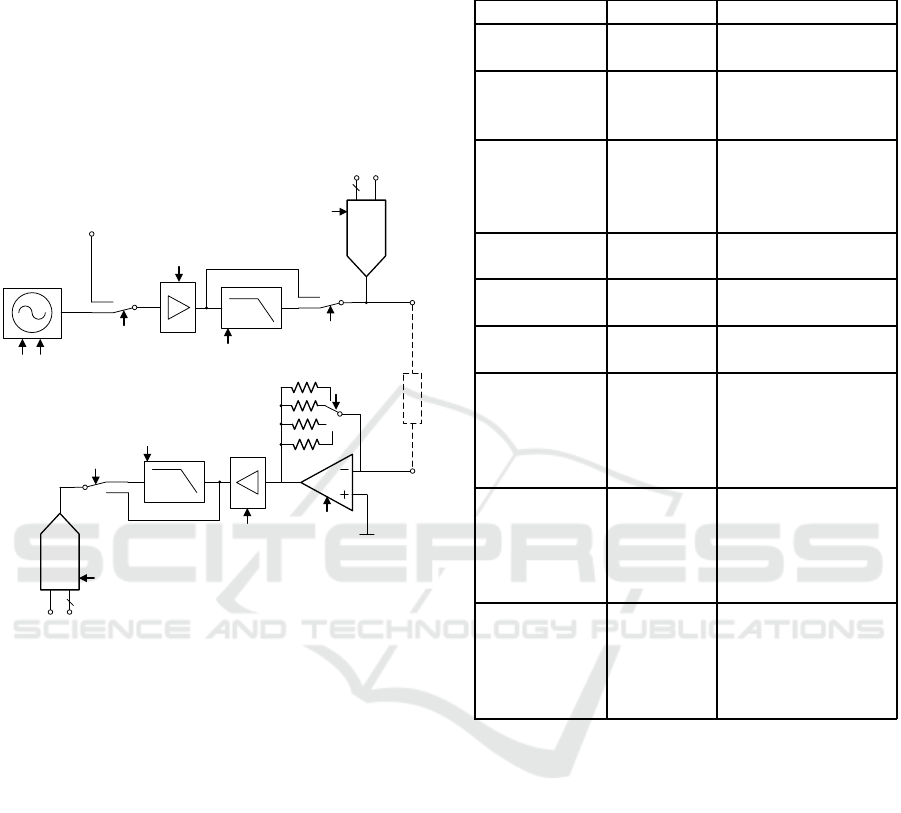
Osc
ExtOsc
LPF1
Gain1
LPF1set
ByPsLPF1
OscSel
LPF2set
ByPsLPF2
ADC10
1
D0...9
EOC1
DUT
I2V
I2Vset
LPF2
Gain2
ADC10
2
D’0...9
EOC2
ClkFreq
ClkLvl
PD
PD
PD
PD
PD
Figure 2: Block diagram of the chip.
The input voltage is provided either by an internal
oscillator or an external source. This input signal is
low-pass filtered and applied to the DUT. The current
is converted to a voltage by the operational amplifier,
and the output signal is applied to another low-pass
filter. The input and output voltages are sampled by
on-chip 10-bit ADCs, or by a National Instruments
PCI-6289 acquisition board.
The power is supplied from 3.3 V and 1.65 V
sources, and the chip draws approximately 5 mW
of power when operating from an external oscillator,
with the low-pass filters enabled, and the ADCs
deactivated.
2.1 Configuration Register
The circuit operation can be adjusted by programming
an on-board 32-bit register. A detailed description of
the configuration bits is shown in Table 1.
The default power-on configuration enables the
internal oscillator, enables the low-pass filters with
unity gain and sets a feedback resistance at 1 MΩ.
Table 1: Description of the configuration register.
Signal Name Description
Reg<0> PD 0: Chip Enabled
1: Chip Disabled
Reg<1:7> ClkFreq 0010001: 39 kHz
1010110: 15 kHz
0011000: 3 kHz
Reg<8:14> ClkLvl 0000001: 1 V
0010100: 500 mV
0010100: 100 mV
1000000: 25 mV
Reg<15> OscSel 0: Internal
1: External
Reg<16> ByPsLPF1 0: LPF1 Enabled
1: LPF1 Disabled
Reg<17> ByPsLPF2 0: LPF2 Enabled
1: LPF2 Disabled
Reg<18:20> LPF1set Gain Adjustment 1
000: Av = 1
110: Av = 2
111: Av = 6
101: Av = 10
Reg<21:23> LPF2set Gain Adjustment 2
000: Av = 1
110: Av = 2
111: Av = 6
101: Av = 10
Reg<24:27> I2Vset Feedback Selection
1010: 10 kΩ
0110: 100 kΩ
0000: 1 MΩ
0011: 10 MΩ
2.2 Internal Oscillator
The ASIC includes an on-board oscillator for
generating the sinusoidal waveforms applied to the
device-under-test. This oscillator is based on a digital
resonator circuit, using oversampling and delta-sigma
modulation techniques (Lu and Roberts, 1994).
The internal oscillator requires an external square
clock source of 12.8 MHz, which can be divided
externally by a factor ranging from 1 to 8 to obtain
lower oscillation frequencies. The output frequency
and amplitude can be programmed by the ClkFreq
and ClkLvl configuration bits on the main register.
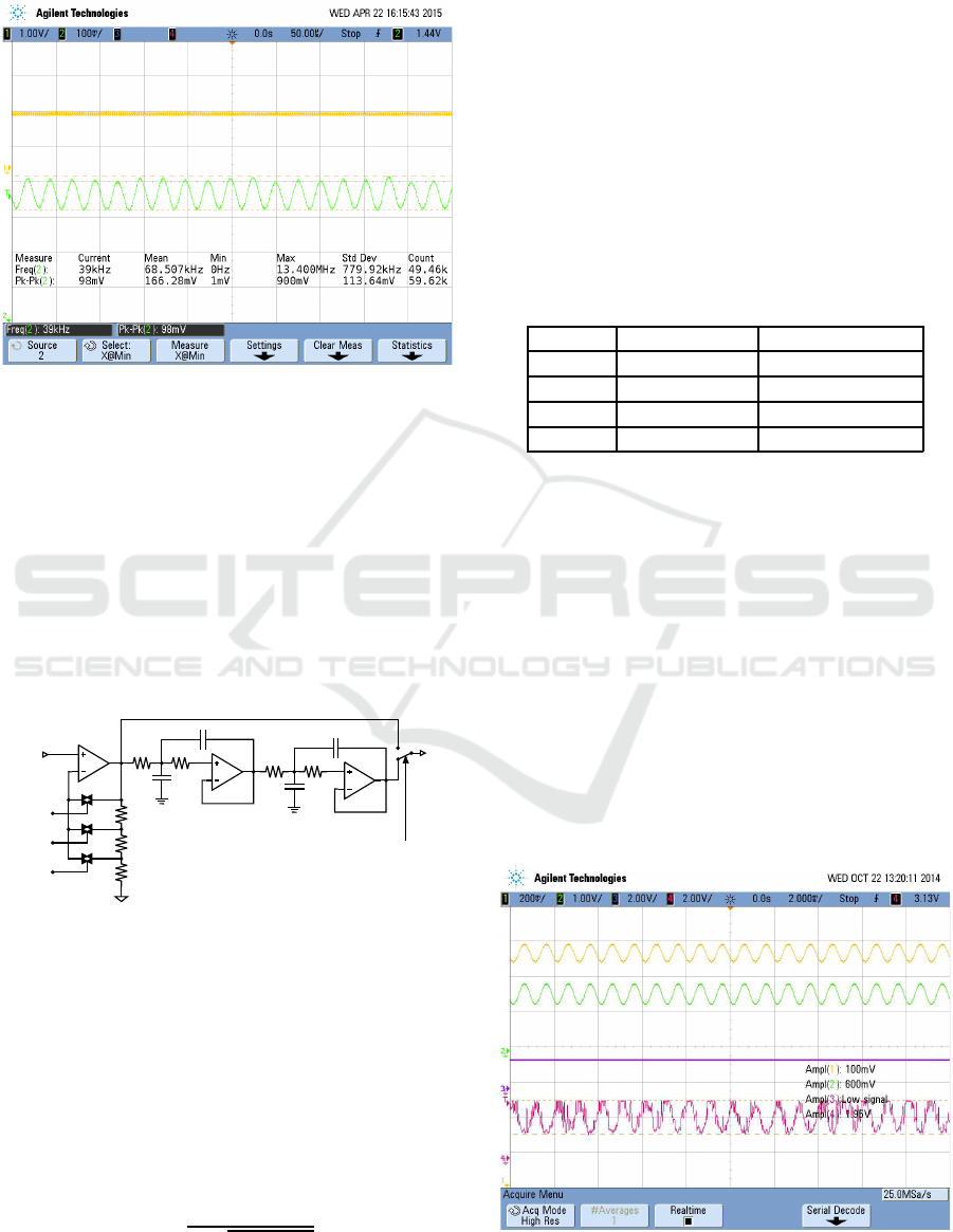
The output voltage of the internal oscillator is
observed in Figure 3 running at 39 kHz with an output
amplitude of 98 mV peak-to-peak.
An external oscillator can be used instead of the
internal oscillator by setting the OscSel bit on the
An Impedance Spectroscopy ASIC for Low-Frequency Characterization of Biological Samples
223
main register. The external oscillator should provide
a sinusoidal wave with a DC offset of 1.65 V.
Figure 3: Oscillator of the chip, running at 39 kHz.
2.3 Low-pass Filter
This block is used to amplify the input signal and filter
any noise from the oscillator, and also to amplify the
output signal after the current-to-voltage conversion.
The low-pass filter block is implemented by a
non-inverting amplifier with adjustable gain, and two
cascaded second-order active low-pass filters with
unity gain. The circuit for this block is shown in
Figure 4.
Vin
Vout
LPFset<0>
LPFset<1>
LPFset<2>
R1 R2
C1
C2
R3 R4
C3
C4
Rg1
Rg2
Rg3
ByPsLPF
Figure 4: Block diagram of the low-pass filters.
The gain of the amplifier can be adjusted to 1, 2,
6 or 10 by setting the corresponding LPF#set<0:2>
bits. If desired, the low-pass filters can be bypassed
by setting the corresponding ByPsLPF# bit in the
main register as well.
The cutoff frequency of each of the filter stages
is calculated with equation 1. For the first filter this
corresponds to f
C1
= 40.146 kHz and for the second
filter f
C2
= 41.094 kHz.
f
C
=
1
2π
√
R
1
R
2
C
1
C
2
(1)
2.4 I2V Converter
The current-to-voltage converter is implemented with
an inverter op-amp. The feedback resistance is
selected using the I2Vset< 0:3> bits of the main
register to adjust the gain depending on the expected
value of the device-under-test.
In order to avoid saturation of this op-amp, the
gain should be set properly so that the output does
not exceed the supply voltage of 3.3 V. This is done
by setting the feedback resistance to a value close to
the DUT, so that the voltage gain is kept lower than
1. This leads to four recommended operation ranges,
displayed in Table 2.
Table 2: Operation ranges for impedance measurement.
R
f
I2Vset<0:3> DUT range
10 kΩ 1010 10 kΩ - 100 kΩ
100 kΩ 0110 100 kΩ - 1 MΩ
1 MΩ 0000 1 MΩ - 10 MΩ
10 MΩ 0011 10 MΩ - 28 MΩ
Impedances lower than 10 kΩ can be measured by
connecting a series resistance to the DUT. The largest
impedance that can be measured is 28 MΩ, and it is
limited by the noise of the circuit, because the output
voltage decreases as the impedance increases.
2.5 Circuit Operation
The output waveforms of the chip in full operation
are shown in Figure 5. From top to bottom, the first
waveform is the input signal, the second is the input
signal after the low-pass filters, the third one is the
input of the operational amplifier (virtual ground) and
the last one is the output signal.
Figure 5: Voltage waveforms of the chip.
BIODEVICES 2016 - 9th International Conference on Biomedical Electronics and Devices
224
The impedance of the connected device-under-test
can be determined from these waveforms by
observing the amplitudes and phases of the
second and the fourth curves, corresponding to
the applied voltage and the output voltage after the
current-to-voltage conversion. This will be addressed
in the following section.
3 IMPEDANCE COMPUTATION
The impedance of the DUT is determined from the
gain of the current-to-voltage converter, calculated
with equation 2. In this equation, R
f
is the selected
feedback resistance described in Table 2.
v
o
=
−R
f
Z
DUT
·v
i
(2)
Since the input and output voltages are pure
sine waves, the Discrete Fourier Transform (DFT) is
used to obtain the fundamental components, with the
advantage of noise filtering. The input and output
voltages are sampled using the National Instruments
PCI-6289 DAQ board with a sampling frequency of
80 kHz per channel.
For implementing the calculations, LabVIEW
was chosen due to the availability of libraries for
digital signal processing, and also because of the
availability of an acquisition board at the Institute,
but the algorithm can be implemented on a high-end
microcontroller or a FPGA with DSP capabilities.
The LabVIEW program enables continuous
real-time monitoring of the impedance of the sample,
and stores the data in a text file. The input parameters
of the LabVIEW program are described in Table 3.
Table 3: Input parameters of the LabVIEW program.
Parameter Description Value
F
S
Sampling frequency 80 kHz
N Number of samples 512
R
f
Feedback resistance 10 kΩ
T Measurement time 30 min
t
S
Sampling delay 1 s
The sampling frequency F
S
is used to acquire the
data and calculate the DFT, using a block size N. The
program keeps running for T minutes and averages
the measurements, producing one impedance point
every t
S
seconds.
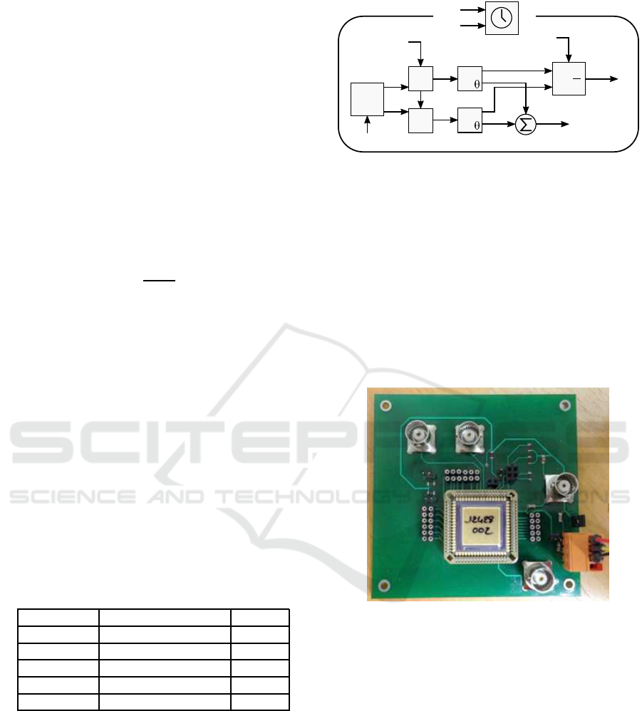
The LabVIEW block diagram used to perform the
calculations is presented in Figure 6.
DAQ
F
F
Z
Z
+
_
Angle(Z)
-Rf
vi
vo
vi
vo
Mag(Z)
N
CH1
CH2
Rf
F
s
T
t
s
Figure 6: LabVIEW program for impedance calculation.
4 MEASUREMENT SETUP
The test board for impedance measurement of
samples is shown in Figure 7. The device-under-test
is connected between the upper-left BNC connectors,
the external oscillator is applied through the right
BNC connector, and the remaining connector on
the lower-right corner is for accessing an on-chip
capacitor array, which is not addressed in the present
document.
Figure 7: Test board for impedance measurements.
Experiments are performed in a commercial
384-well plate from Corning Inc., using two pins as
microelectrodes. The electrodes are of copper and
they are changed for every measurement, as they tend
to get oxidized and damaged by electrolysis.
The electrodes are shown in Figure 8.
In the following section, yeast experiments were
carried out with a commercial LCR meter and with
the ASIC. The goal of the experiment is to observe
the impedance of the culture as the cells grow.
An Impedance Spectroscopy ASIC for Low-Frequency Characterization of Biological Samples
225
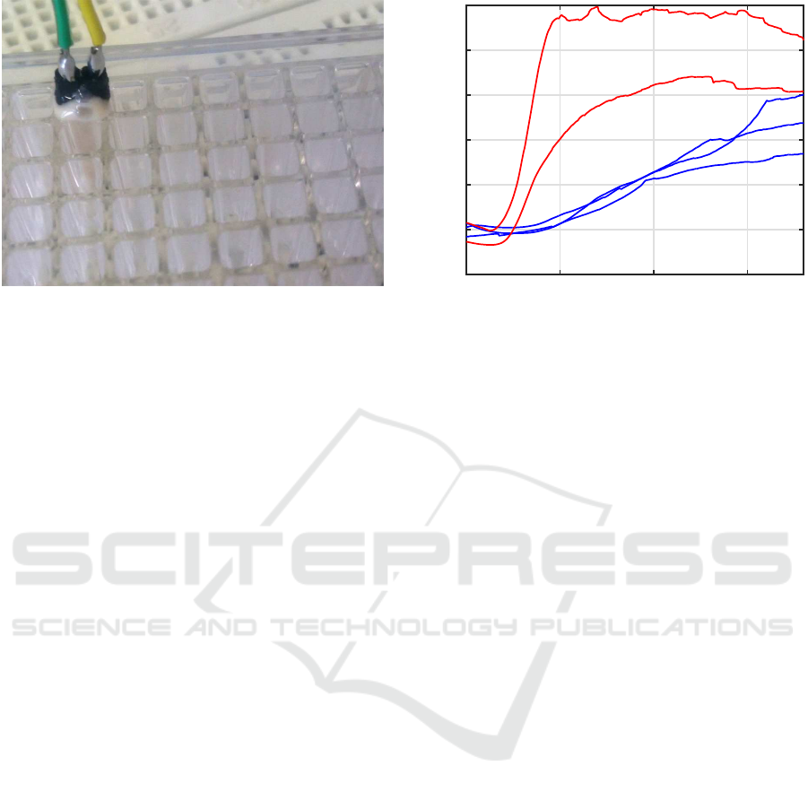
Figure 8: Test chamber with electrodes.
5 YEAST EXPERIMENTS
The growing process of yeast cells can be either
synchronous or asynchronous (Asami et al., 1999). In
the first case, every cell of the culture is in the same
growth stage and therefore the cellular cycles can be
seen in the impedance curve. In the asynchronous
process, cells are not necessarily in the same growth
stage and therefore cycles are not as visible as in the
synchronous case.
In the present experiment, the cells are placed
in well plates at room temperature, without any
controlled environmental condition, and the growth
follows an asynchronous process. Therefore it is not
possible to observe the reproduction cycles.
5.1 Agilent 4284a LCR Meter
The impedance of a yeast cell culture was measured
with an Agilent 4284a LCR Meter to observe the
growth pattern of the impedance of the cells with
standard commercial equipment.
The test chamber is filled with yeast cells until half
of its height (approximately 6 mg), and the rest of the
well is filled either with tap water or with sugar water.
The sugar concentration was not measured, but is
different for the two experimental curves shown in
Figure 9. The blue curves describe the growth of
yeast cells in tap water, and the red curves describe
the impedances of cell cultures in sugar water.
As expected, the growth is accelerated by the
inclusion of sugar in the samples. The difference
between the two red curves arises from the different
glucose concentrations.
Time [s]
0 500 1000 1500
Impedance [kΩ]
0
1
2
3
4
5
6
Figure 9: Impedance of yeast cell cultures in tap water
(blue) and in sugar water (red), measured with an Agilent
4284a LCR meter for 30 minutes.
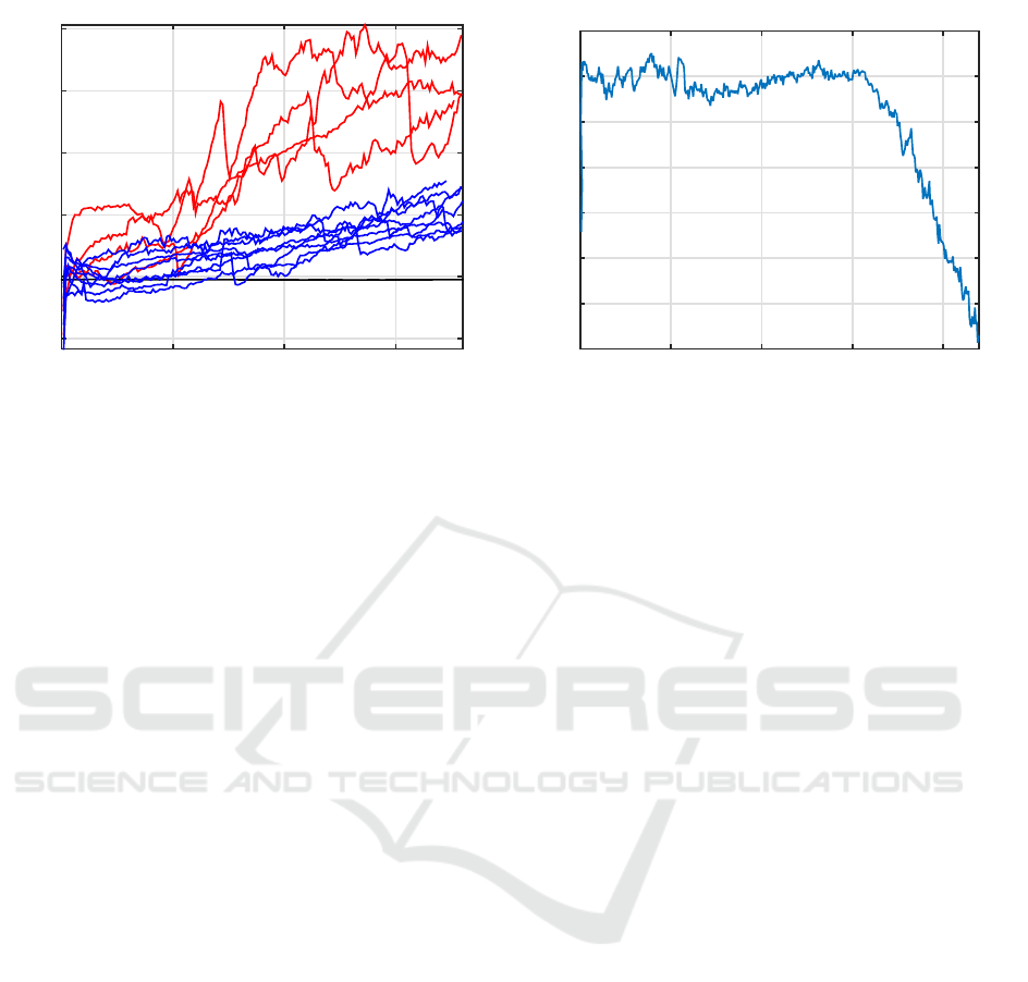
5.2 Yeast Experiments with the ASIC
In this section, the ASIC is used to perform the
impedance recording of eight yeast samples.
The ASIC is configured to operate with an
external oscillator, unity gain at the amplifiers, the
low-pass filters activated, and a resistance of 20 kΩ
in series with the DUT, to operate the chip in the
proper range according to Table 2. This resistance is
necessary because the chip is not suitable to measure
impedances under 10 kΩ.
The external oscillator provides a sine wave with
a frequency of 2 kHz, an amplitude of 100 mV
peak-to-peak and a DC offset voltage of 1.65 V. The
DC offset can be adjusted during the experiment to
operate the chip in the linear region.
The experimental measurements of yeast cell
growth are shown in Figure 10. The measurements
were carried out for thirty minutes. This plot shows
the impedance patterns for eight samples in tap
water (blue), five samples in sugar water (red) and
a reference line showing the impedance of water
without cells (black).
These measurements are similar to Figure 9, and
in both scenarios, the impedance of the samples is
increasing as the cells grow. The cells in presence
of glucose grow faster than the cells immersed only
in tap water.
With these measurements, the functionality of
the chip has been tested. In the next section, the
impedance of porcine chondrocytes is measured to
provide more experiments with biological material.
BIODEVICES 2016 - 9th International Conference on Biomedical Electronics and Devices
226
Time [s]
0 500 1000 1500
Impedance [kΩ]
20
25
30
35
40
45
Figure 10: Impedance of yeast cell cultures in tap water
(blue) and in sugar water (red), plotted together with the
impedance of tap water without cells (black) as reference.
The 20 kΩ series resistance can be subtracted only if the
phase information is available.
6 PORCINE CHONDROCYTES
A second type of cells, the porcine chondrocytes,
were used in the experiments with the ASIC. The
concentration of cells in the sample is around
1.45×10
6
cells/ml when immersed in Dulbecco’s
Modified Eagle Medium (DMEM). The cells were
placed in a standard 384-well plate with a well size
of 80 µL. The impedance of one sample was recorded
for one hour using the same measurement setup and
applied voltages as for the yeast cell experiments. The
result is shown in Figure 11.
The impedance remains constant for the first 3000
seconds, and after this time, it starts to decrease.
One reason for this behavior is the cell death due
to copper contamination. The test electrodes used for
this paper were made of copper, and it is possible
that copper ions are being released into the medium.
Copper is a toxic material for the cells.
Another possibility is the deposition of cells over
time at the bottom of the container. The impedance
decreases because the concentration at the top part of
the container is reduced.
7 CONCLUSIONS
Impedance measurements of biological samples have
been performed with the ASIC. The operation of the
chip was confirmed by measuring the impedance of
yeast cell samples and of porcine chondrocytes.
Time [s]
0 1000 2000 3000 4000
Impedance [kΩ]
17
18
19
20
21
22
23
24
Figure 11: Impedance of porcine chondrocytes in series
with a 20 kΩ resistance. The phase information is necessary
to subtract this resistance from the complex impedance of
the sample.
The ASIC was able to detect the difference
between a yeast cell culture in tap water and another
cell culture with sugar water, where the cell growth
rate is faster. This was verified in Figure 10.
Also, the chip was able to measure the impedance
of porcine chondrocytes and detected a decrease of
the impedance after 3000 seconds, which could be
related with cell death or cell deposition at the bottom
of the container.
For future experiments, it is recommended to use
electrodes of platinum or Ag/AgCl, since the copper
pins used on this study can get oxidized and affected
by electrolysis, changing the composition of the DUT
and even damaging the cells.
With these preliminary studies, we conclude that
the ASIC can be used to monitor the impedance of
biological samples over time.
ACKNOWLEDGEMENTS
The authors would like to thank Dr. Christiane
Goepfert from the Institute of Bioprocess and
Biosystems Engineering, for providing the materials
and support for the porcine chondrocyte experiments.
REFERENCES
Alvarenga, R. L. and Souza, M. N. (2007). Estimation of
the Lactate Threshold Using Bioelectrical Impedance
Spectroscopy: A New Noninvasive Method. In 2007
29th Annual International Conference of the IEEE
An Impedance Spectroscopy ASIC for Low-Frequency Characterization of Biological Samples
227

Engineering in Medicine and Biology Society, volume
2007, pages 3052–3055. IEEE.
Asami, K., Gheorghiu, E., and Yonezawa, T. (1999).
Real-Time Monitoring of Yeast Cell Division by
Dielectric Spectroscopy. Biophysical Journal,
76(6):3345–3348.
Giaever, I. and Keese, C. R. (1984). Monitoring fibroblast
behavior intissue culture with an applied electric field.
Proceedings of the National Academy of Sciences,
81(12):3761–3764.
Giaever, I. and Keese, C. R. (1986). Use of Electric Fields
to Monitor the Dynamical Aspect of Cell Behavior
in Tissue Culture. IEEE Transactions on Biomedical
Engineering, BME-33(2):242–247.
Hossain, Q. D. and Dhar, S. K. (2013). Characterization of
Physiological Glucose Concentration Using Electrical
Impedance Spectroscopy. International Journal of
Computer Science, 10(1):105–111.
Keysight (2015). Impedance Measurement Handbook.
Keysight Technologies, https://www.keysight.com/,
4th edition.
Lu, A. and Roberts, G. (1994). A High-Quality Analog
Oscillator Using Oversampling D/A Conversion
Techniques. IEEE Transactions on Circuits and
Systems, 41(7):437–444.
BIODEVICES 2016 - 9th International Conference on Biomedical Electronics and Devices
228
