
Design and Test of SiPM Structures in CMOS Technology
N. D’Ascenzo
1,2
, V. Saveliev
1,2
and Q. Xie
1,2
1
Hiazhong University of Science and Technology, Wuhan, China
2
Wuhan National Laboratory for Optoelectronics, Wuhan, China
Keywords:
Silicon Photomultiplier, Avalanche Breakdown Structures, CMOS.
Abstract:
In this paper we report our results on the influence of STI guard ring structures on the design and performances
of SiPM with n+p microcells. Two types of SiPM detection structures were designed and fabricated in standard
CMOS technology production line. A key-point of our study is the mathematical modelling and simulation of
the structure using the well-estabilished CMOS technology simulation frameworks and models. We analyse
the electric field and ionization coefficients of the designed structures at breakdown voltage. In addition,
experimental characterization of the fabricated SiPM including current characteristics, CV characteristics was
measured and analysed in order to identify the best structure for a correct CMOS implementation of the SiPM
with STI guard rings.
1 INTRODUCTION
The Silicon Photomultiplier (SiPM) had an impres-
sive development in the last decade ((Saveliev and
Golovin, 2000; Saveliev, 2010; D’Ascenzo and
Saveliev, 2012; D’Ascenzo et al., 2015; Golovin and
Saveliev, 2004)). It is a semiconductor detector con-
sisting of an array of space-distributed micro-sensors.
Each micro-sensor is capable of detecting a single
quantum of light and the array is detecting a photon
flux. The structure of a micro-cell is based on a n
+
p or
p
+
n junction operated in avalanche breakdown mode.
A resistor is placed in series of each micro-sensor,
integrated in the chip, in order to passive quench the
avalanche. The miniature size of 1 mm
2
, the high
achievable density of microcells of approximately
1000/mm
2
, the low bias voltage, the radiation hard-
ness and insensitivity to the magnetic field satisfy
the operational conditions of a variety of applications
ranging from High Energy Physics to Homeland Se-
curity and Nuclear Medicine. Similar structures are
also known as arrays of large number of single pho-
ton avalanche diodes (SPAD) (Charbon et al., 2013;
Charbon, 2012; Zappa et al., 2007).
The recent advances in the conception of the SiPM
are based on the investigation of the possibility of a
full implementation of the photo-detector within stan-
dard CMOS. The SiPM design is in fact compatible
with the standard available CMOS technology. The
implementation of the SiPM in standard CMOS tech-
nology enables the monolithic integration of read-
out electronics and photo-detector on the same chip,
with significant reduction of power consumption and
simplification of the operational conditions. Further
progress and development of even more sophisticated
detector concepts will be also enabled by this pos-
sibility. Based on this idea an innovative position
sensitive pixelated sensor for the detection and mea-
surement of the coordinates of ionising particles with
high precision has been proposed (D’Ascenzo et al.,
2014). The silicon avalanche pixel sensor (APiX)
is based on the vertical integration of avalanche pix-
els connected in pairs and operated in coincidence in
fully digital mode and with the processing electronics
embedded on the chip. Moreover the use of standard
CMOS technology facilities would in fact reduce the
cost of the detector, allowing an effective and stable
mass production for industry use.
However, SiPM can suffer of localized breakdown
conditions on the locally concentrated high electric
field at the junction edges. The use of guard ring
structures around the sensitive area of each micro-
cell is in this respect mandatory in order to obtain a
uniform electric field across the whole sensitive area.
The CMOS technology offers few possibilities of im-
plementing such guard rings ( (ITRS, 2003; Lee et al.,
2012; Izhaky et al., 2006)). It is possible to surround
the highly doped n+ or p+ areas with a weakly doped
n- or p- well in order to smooth the resulting elec-
tric field at the edge of the junction. It is also possi-
D’Ascenzo, N., Saveliev, V. and Xie, Q.
Design and Test of SiPM Structures in CMOS Technology.
DOI: 10.5220/0005746702130220
In Proceedings of the 4th International Conference on Photonics, Optics and Laser Technology (PHOTOPTICS 2016), pages 215-222
ISBN: 978-989-758-174-8
Copyright
c
2016 by SCITEPRESS – Science and Technology Publications, Lda. All rights reserved
215
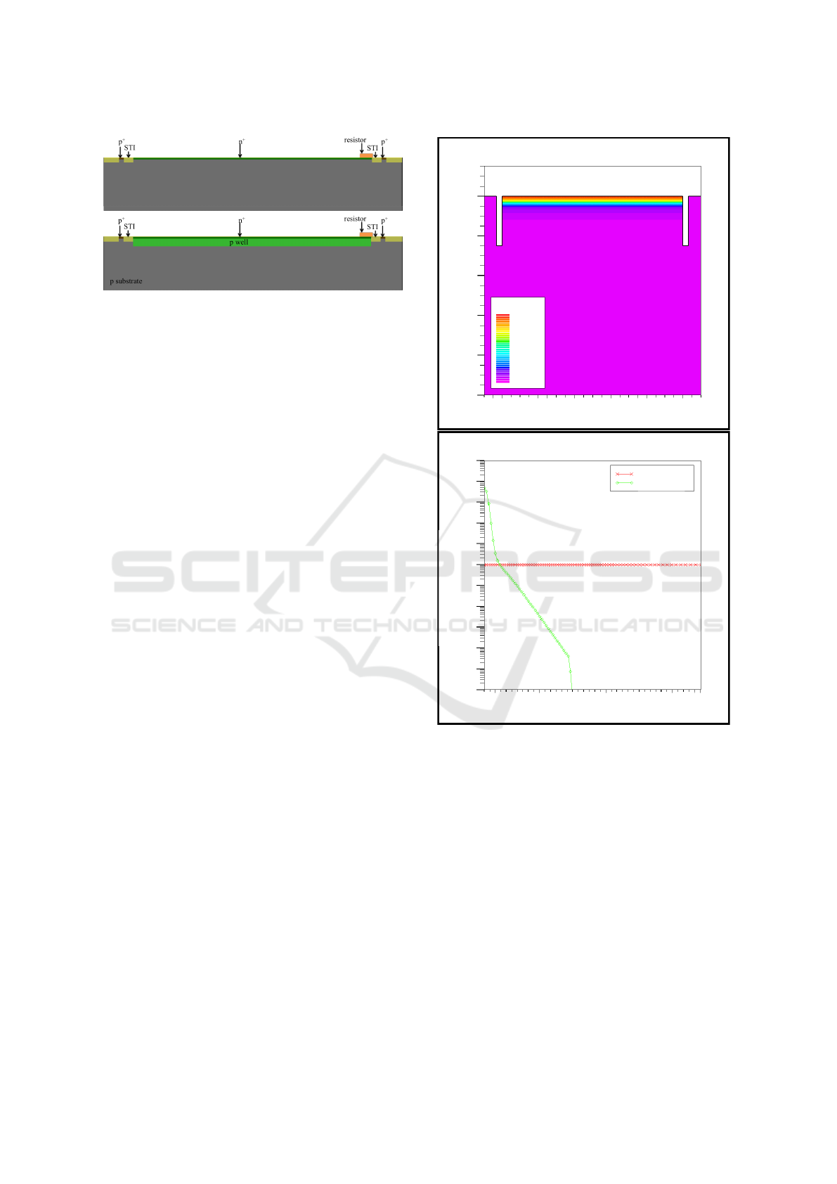
Figure 1: Cross section of the two types of SIPM structures
in 180 nm CMOS technology: n
+
/psub structure (up) and
n
+
/pwell (down). Both structures are with STI guard rings.
ble to use Shallow Trench Isolation (STI) around the
highly doped n+ or p+ areas in order to remove the
discontinuity in doping concentration at the edges of
the structure.
In this paper we report our results on the influ-
ence of STI guard ring structures on the design and
performances of SiPM on the example of n+p micro-
cell structure. Two types of SiPM detection structures
were designed and fabricated in standard CMOS tech-
nology production line. Using mathematical mod-
elling and simulation, we analyse their electric field
and ionisation coefficients at breakdown voltage .
In addition, experimental characterisation of the fab-
ricated SiPM including current characteristics, CV
characteristics was measured and analysed in order to
identify the best structure for a correct CMOS imple-
mentation of the SiPM with STI guard rings.
2 DEVICE STRUCTURES AND
SIMULATION RESULTS
The cross sections of the two types of SiPM structures
fabricated in 180 nm CMOS technology are shown
in Fig. 1. The first structure consists of a np junc-
tion formed with an n
+
implantation on the silicon
substrate. The second structure consists of a np junc-
tion formed with an n
+
implantation on a p-well. STI
guard rings are placed around the n
+
implantation,
between the n
+
and p
+
implantation, according to the
standard CMOS rules. The output current from the
junction flows through a quenching resistor with typ-
ical value ranging between 500 kΩ and 1 MΩ. The
resistor is obtained with High Resistive Polysilicon
(HRP) technology also available at CMOS foundry.
The sensitive area consists of a 50 × 50 µm
2
window,
corresponding to the n
+
implantation. The design fol-
lows strongly the design rules of the 180 nm CMOS
technology used for design and production.
We perform the device mathematical modelling
Pixel Length [Micrometer]
0
10 20 30 40
50 60
Pixel Width [Micrometer]
2
1.6
1.2
0.8
0.4
0
Total Doping
20.5
18
17
19.5
Pixel Width [Micrometer]
0 0.2 0.4 0.6
0.8 1.0 1.2
1.4 1.6 1.8
10
11
10
12
10
13
10
14
10
15
10
16
10
17
10
18
10
19
10
20
10
21
10
22
Concentration [cm
-3
]
Acceptor
Donor
Figure 2: Total doping profiles of the simulated n
+
/psub
structure. Transverse view (top panel) and cross sectional
view along the central line at length 30 µm (bottom panel).
within the simulation framework SILVACO (Silvaco).
The aim of the mathematical model is the extraction
of the influence of the STI guard rings on the electric
field profiles for both structures of the CMOS SiPMs.
The doping profiles are obtained with a detailed de-
vice process simulation, corresponding to the indica-
tions of the production facility.
The cross sectional view and the profile of the to-
tal doping of the n
+
/psub and n
+
/pwell structures is
shown on Fig. 2, 3. The doping concentration of the
p-substrate is about 10
17
cm
−3
, The obtained p-well
concentration ranges between 10
17
cm
−3
at the sur-
face and a maximal value of about 4.5 × 10
17
cm
−3
at
a depth of 0.6 µm. The concentration of the n
+
im-
PHOTOPTICS 2016 - 4th International Conference on Photonics, Optics and Laser Technology
216
Pixel Width [Micrometer]
2
1.6
1.2
0.8
0.2
0
0.4
0.6
1.0
1.4
1.8
Pixel Length [Micrometer]
0
10 20 30 40
50 60
Total Doping
20.5
19.2
17.5
16.3
10
11
10
12
10
13
10
14
10
15
10
16
10
17
10
18
10
19
10
20
10
21
10
22
Concentration [cm
-3
]
Pixel Width [Micrometer]
0.2 0.4 0.6
0.8 1.0 1.2
1.4 1.6 1.8
Acceptor
Donor
Figure 3: Total doping profiles of the simulated n
+
/pwell
structure. Transverse view (top panel) and cross sectional
view along the central line at length 30 µm (bottom panel).
plantation peaks at 4 × 10
21
cm
−3
.
The simulation of the DC and AC device includes the
solution of the Boltzmann transport equation, includ-
ing the auger recombination model and the Selber-
herr’s model (Sze and K.N., 2007) for the description
of the impact ionisation process. The Poisson equa-
tion is solved dynamically for the determination of the
strength of the electric field across the junction.
The numerical simulation allows studying the ef-
fects of localised breakdown conditions due to the lo-
cal geometry of the junction and allows designing the
guard rings structures for the correction of such prob-
lem.
As an example, we first study the properties of
Pixel Length [Micrometer]
0
10 20 30 40
50 60
Pixel Width [Micrometer]
2
1.6
1.2
0.8
0.4
0.2
Electric Field
7.89e4
2.31e5
4.2e5
7.89e5
Pixel Length [Micrometer]
0
10 20 30 40
50 60
Pixel Width [Micrometer]
2
1.6
1.2
0.8
0.4
0
0.2
0.6
1.0
1.4
1.8
Electric Field
7.08e4
2.83e5
6.37e5
7.08e5
Figure 4: Electric field strength of the simulated
n
+
/psub(top) and n
+
/pwell (bottom) structure without STI.
The non uniformity of the electric field on the corners of the
junction is visible.
the detection structures without STI. The cross sec-
tional view of the electric field at breakdown across
the junction for both structures without STI is shown
on Fig. 4. The electric field without STI exhibits
an upper value respectively of about 8 × 10
5
V/cm
in both structures on a localised spot at the junction
corners. The strength of the electric field along the
junction is uniform with a value of about respectively
4.5 × 10
5
V/cm and 6 × 10
5
. Thus, in a structure
without STI trenches, the electric field strength on the
junction periphery exceeds of a factor 2 the electric
field strength along the sensitive area of the diode,
causing strong non-uniformity in light detection ef-
Design and Test of SiPM Structures in CMOS Technology
217
Pixel Length [Micrometer]
0
10 20 30 40
50 60
Pixel Width [Micrometer]
2
1.6
1.2
0.8
0.4
0
Electric Field
5.24e4
2.1e5
4.2e5
5.2e5
Pixel Width [Micrometer]
0.2 0.4
0.6 0.8 1.0
1.2 1.4 1.6 1.8
0
0
1
2
3
4
5
6
7
8
9
10
Pixel Width [Micrometer]
Electric Field [V/cm]
Electric Field
Figure 5: Electric field strength of the simulated n
+
/psub
structure. Transverse view (top panel) and cross sectional
view along the central line at length 30 µm (bottom panel).
ficiency. In other words, the dominant sensitive part
reduces in this case only to the edges of the junction.
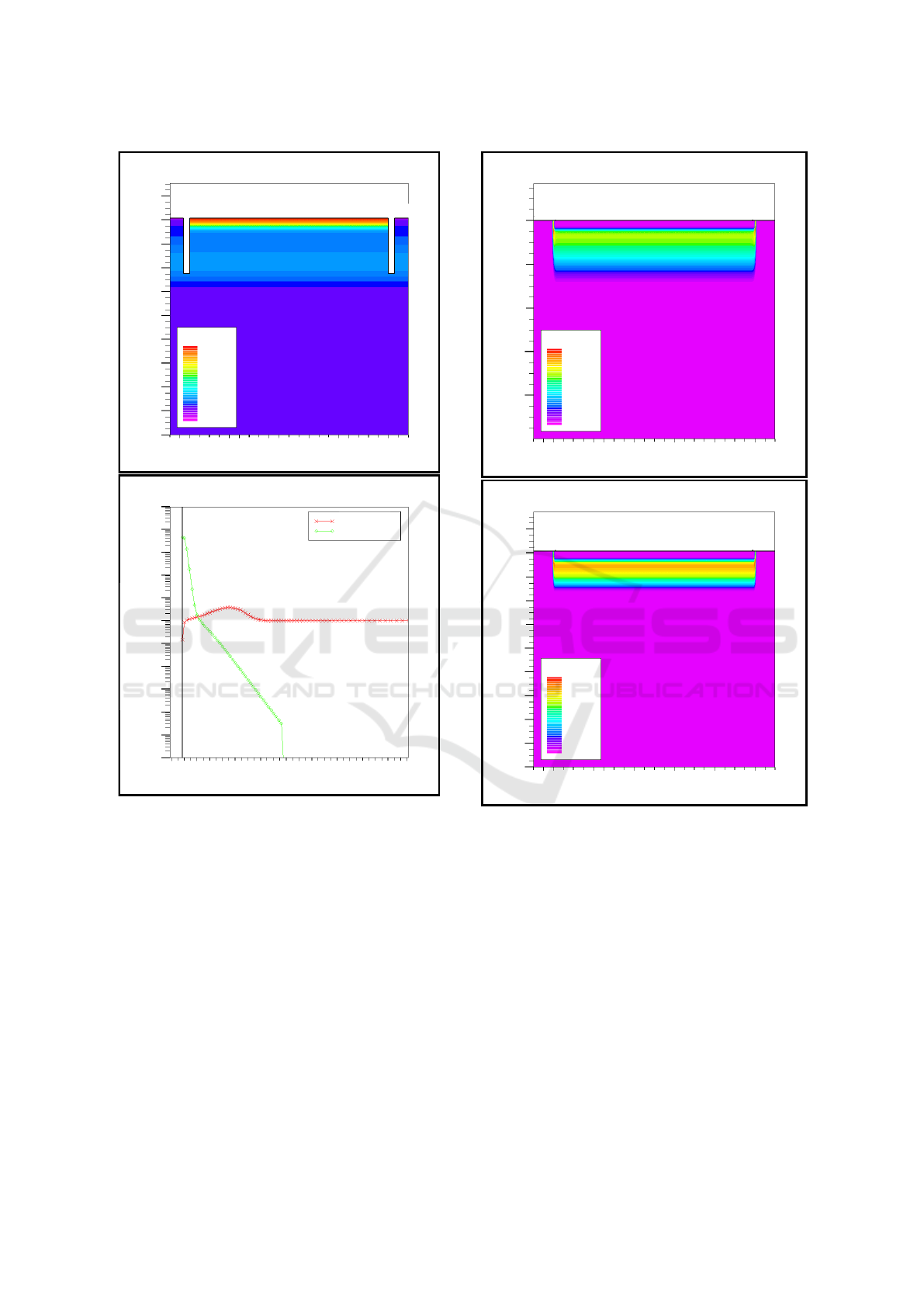
The introduction of the STI guard rings improves
the situation significantly. The cross sectional view
and the profile of the electric field across the junc-
tion at breakdown is shown in Fig. 5, 6 respectively
for the n
+
/psub and n
+
/pwell structures at their re-
spective breakdown voltage. The corner effect at the
edges of the junction disappears and the electric field
is uniform along the whole junction. The maximal
electric field obtained with the n+/psub structure is
about 5.5 × 10
5
V/cm at about 0.2 µm from the sur-
face, while the maximal electric field obtained with
the n+/pwell structure is about 6.4 × 10
5
V/cm at
Pixel Length [Micrometer]
0
10 20 30 40
50 60
Pixel Width [Micrometer]
2
1.6
1.2
0.8
0.4
0
0.2
0.6
1.0
1.4
1.8
Electric Field
6.04e4
2.43e5
4.33e5
6.04e5
Pixel Width [Micrometer]
0.2
0.4 0.6 0.8
1.0 1.2 1.4 1.6
1.8
0
0
1
2
3
4
5
6
7
8
9
10
Pixel Width [Micrometer]
Electric Field [V/cm]
Electric Field
Figure 6: Electric field strength of the simulated n
+
/pwell
structure. Transverse view (top panel) and cross sectional
view along the central line at length 30 µm (bottom panel).
about 0.1 µm from the surface.
From a comparison between Fig. 5 and Fig. 6 we
observe that, due to the lower doping concentration
of the n
+
/psub structure respect to the n
+
/pwell struc-
ture, the junction width of the first structure is wider
than the second one, being the widths respectively
about 0.5 µm and 0.3 µm.
The working principle of the SiPM is the pas-
sive quenching. The voltage drop through a quench-
ing resistor causes the bias on the diode to decrease
and stops the avalanche process occurring in the
junction. This is in opposition with the traditional
avalanche photodiodedes, which are operated in a
self-quenching mode, though statistical fluctuation of
PHOTOPTICS 2016 - 4th International Conference on Photonics, Optics and Laser Technology
218
Pixel Length [Micrometer]
0
10 20 30 40
50 60
Pixel Width [Micrometer]
2
1.6
1.2
0.8
0.4
0.2
Ionization C.
7.29e3
2.91e4
5.83e4
7.29e4
Pixel Length [Micrometer]
0
10 20 30 40
50 60
Pixel Width [Micrometer]
2
1.6
1.2
0.8
0.4
0.2
Ionization C.
3.05e3
1.22e4
2.44e4
3.05e4
Figure 7: Impact ionisation coefficient for electron (top)
and holes (bottom) in n
+
/psub structure.
the avalanche. In other words, the gain of a SiPM is
determined uniquely by the quenching resistor. It is
thus needed to operate the detector in a regime, where
both carriers contribute to the avalanche process, in
order to develop a self-sustaining avalanche. In other
words the ionisation coefficient of both electrons and
holes needs to be of the same order of magnitude for
a correct operation of the SiPM.
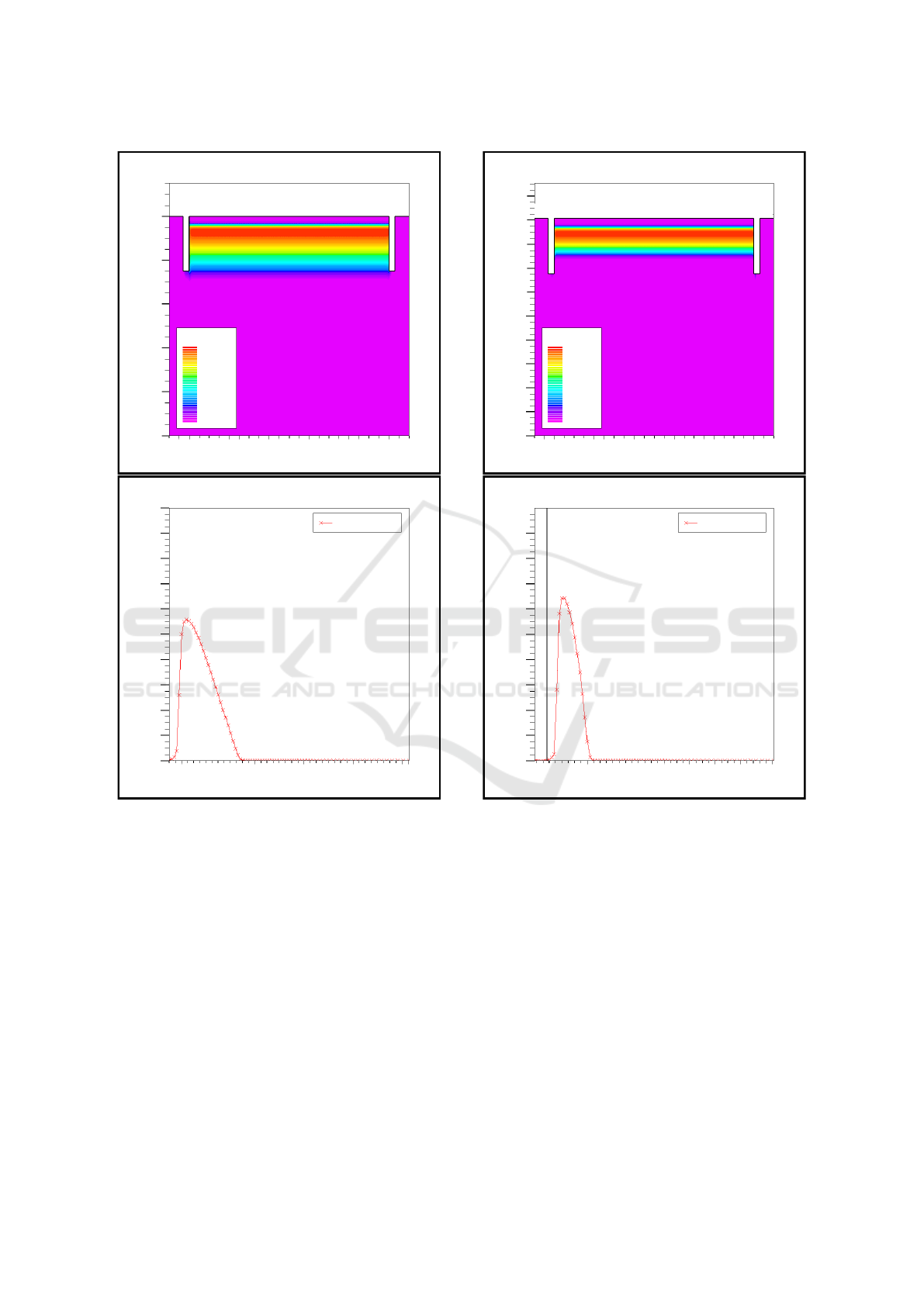
The ionisation coefficient for electron and holes is
calculated in the simulation and is shown on Fig. 7,
Fig 8 and Fig. 9 for respectively the n
+
/psub and
n
+
/pwell structures.
In correspondence with the electric field, the ion-
isation coefficient of electron and holes is uniform
Pixel Length [Micrometer]
0
10 20 30 40
50 60
Pixel Width [Micrometer]
2
1.6
1.2
0.8
0.4
0.2
Ionization C.
9.76e3
3.9e4
7.81e4
9.76e4
0
0.6
1.0
1.4
1.8
Pixel Length [Micrometer]
0 10 20 30
40 50 60
Pixel Width [Micrometer]
2
1.6
1.2
0.8
0.4
0.2
Ionization C.
4.55e3
1.82e4
3.18e4
4.55e4
0
0.6
1.0
1.4
1.8
Figure 8: Impact ionisation coefficient for electron (top)
and holes (bottom) in n
+
/pwell (bottom) structure.
along the junction for both structures. At the break-
down, the maximal value of the ionisation coefficient
of electron and holes in the n
+
/psub structure is re-
spectively about 7.8×10
5
and 3.2 × 10
5
, while in the
n
+
/pwell structure it reaches respectively 1.1×10
6
and 5 × 10
5
. The comparison between the two struc-
tures allows to conclude that at the breakdown the im-
pact ionisation of the n
+
/psub is slightly lower than
the impact ionisation for the he n
+
/pwell structure. In
fact the electric field strength is slightly lower in the
first case. Moreover, we observe that in both struc-
tures the electron and holes ionisation coefficient is
of the same order of magnitude, the holes ionisation
coefficient being smaller than the electrons one. Thus,
we suggest to optimise the stabilisation of the detec-
Design and Test of SiPM Structures in CMOS Technology
219
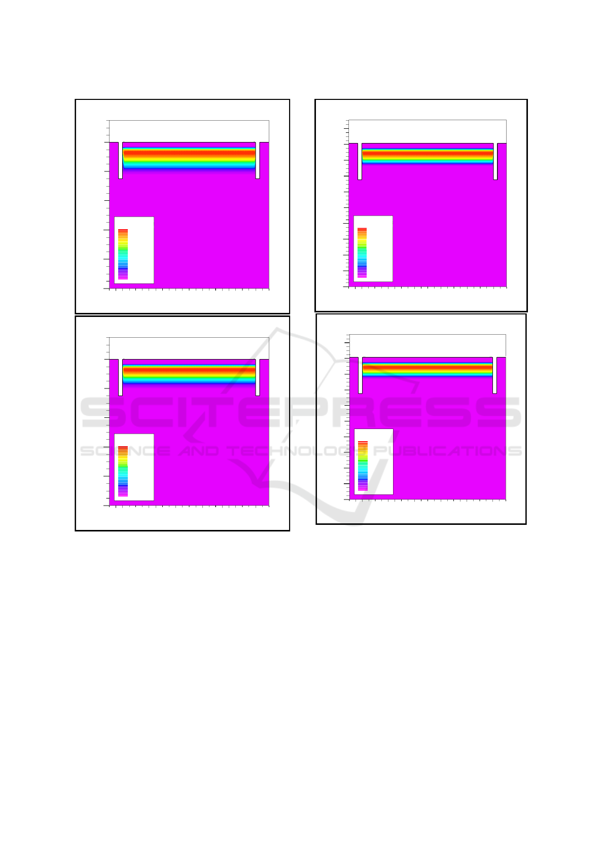
Pixel Width [Micrometer]
0 0.2 0.4 0.6
0.8 1.0 1.2
1.4 1.6 1.8
0
1
2
3
4
5
6
7
8
Ionization coefficient [/cm]
Electron
Holes
Pixel Width [Micrometer]
0.2 0.4
0.6 0.8 1.0
1.2 1.4 1.6 1.8
0
2
4
6
8
Ionization coefficient [/cm]
Electron
Holes
10
Figure 9: Impact ionisation coefficient for electron and
holes in n
+
/psub(top) and n
+
/pwell (bottom) structure.
tor operation in both structures at least 1 V above
the breakdown voltage, in order to further increase
the ionisation coefficient of the holes. Such region is
out of reach for the mathematical model implemented
here, and in the real application is achieved with a sta-
bilisation of the SiPM through the passive quenching
mechanism.
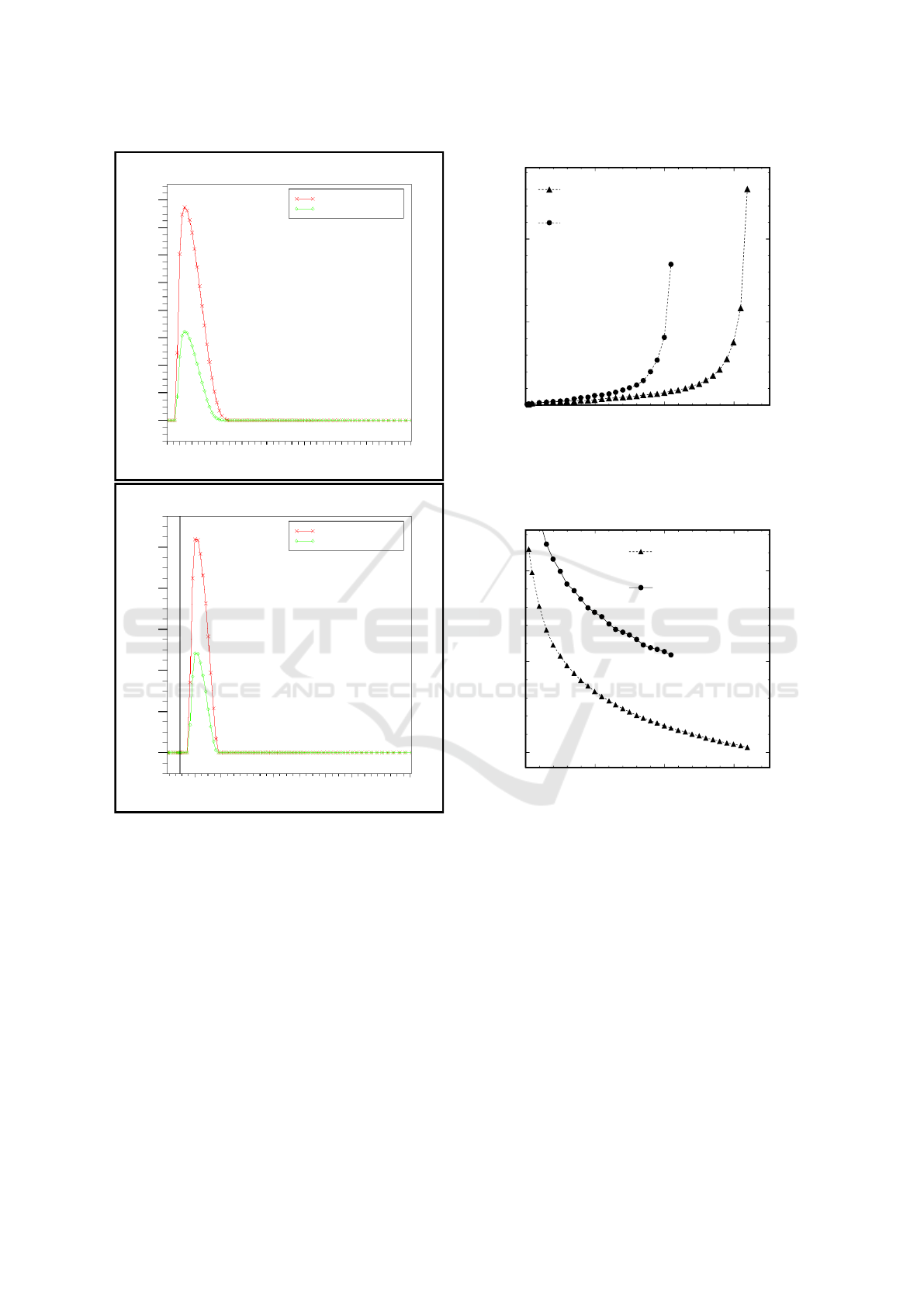
The IV characterization of the structure is shown
on Fig 10 for both structures under analysis. The
n
+
/psub structure exhibits a breakdown at around
15.5 V, while the the n
+
/psub structure exhibits a
breakdown at around 10.5 V. The higher breakdown
voltage of the n
+
/psub is due to the lower average
concentration of the p substrate in comparison with
Bias Voltage [V]
0 5 10 15
I [A]
0
10
20
-12
10×
/psub structure
+
n
/pwell structure
+
n
Figure 10: Mathematical modelling: IV characterisation of
the SiPM structures.
Bias Voltage [V]
0 5 10 15
C [F/mum]
10
20
30
-15
10×
/psub structure
+
n
/pwell structure
+
n
Figure 11: Mathematical modelling: CV characterisation of
the SiPM structures.
the well concentration.
Finally the CV characterisation of the structure is
shown on Fig. 11 for both structures under analysis.
The capacitance of the structures is calculated in an
ac analysis at 1 kHz until the breakdown voltage of
the structure is reached. We observe that the capaci-
tance of the n
+
/psub structures is lower than the ca-
pacitance of the n
+
/pwell structures of approximately
a factor 2 at the breakdown voltage. This corresponds
to the observation that the width of the junction is in
the n
+
/psub structure is approximately twice as larger
as in the n
+
/pwell structure.
PHOTOPTICS 2016 - 4th International Conference on Photonics, Optics and Laser Technology
220
3 EXPERIMENTAL RESULTS
SiPM detectors were designed and fabricated in a
standard 180 nm CMOS process on Multi Project
Wafer according to the detector structures shown in
the previous section. The obtained photodetectors
consist of a 1 mm
2
array of microcells. Each micro-
cell has a sensitive area of 50 µm. Two different sam-
ples on the basis of n
+
/psub and n
+
/pwell structures
were fabricated. DC and AC measurements were per-
formed on wafer after production in a controlled opti-
cal setup allowing for a characterisation in controlled
dark environment.
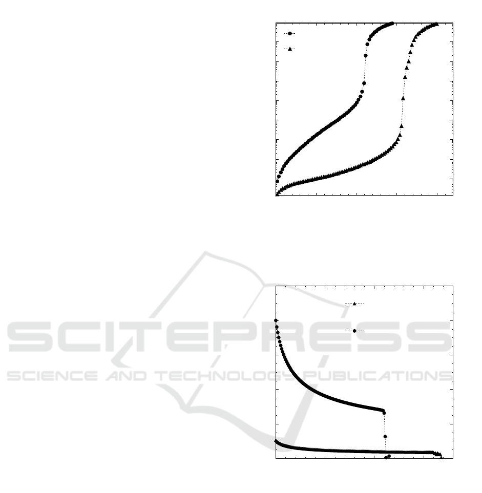
The IV curves measured in dark condition for the
n
+
/psub and n
+
/pwell SiPM are shown on Fig. 12.
We measure a breakdown voltage respectively of
15.5 V and 10.5 V, which confirms the prediction of
the mathematical model and simulation.
We observe that the n
+
/pwell structure exhibits
enhanced dark current than the n
+
/psub structure.
This is probably due to enhanced tunnelling effects
at the edges between the well and the STI. Further in-
vestigation is needed in order to understand these ad-
ditional components of the dark current in well struc-
tures. However, the dark current level is well below
the breakdown current. After the breakdown voltage,
the quenching resistor acts as a current limiter, af-
fecting the slope of the IV curve and stabilising the
SiPM response. The enhancement of the dark current
in n
+
/pwell structures could hence impact on the sin-
gle photon resolution only on a limited extent, causing
only an higher expected dark rate of the device.
The CV characterization of the photodetectors at
1 kHz is shown on Fig. 13. The capacitance at break-
down is measured respectively as 0.15 × 10
−9
F and
0.3 × 10
−9
F for the n
+
/psub and the n
+
/pwell struc-
tures. Although the absolute value of these num-
bers refer to the full array of microcells and can not
be compared with the simulation results, the rela-
tive strength of the capacitance in the two cases is in
agreement with the mathematical model expectation.
In fact we observe that the ration between the capac-
itance at breakdown for the two junctions is approx-
imately a factor 2, which agrees with the mathemati-
cal model estimation of the difference in the junction
width.
4 CONCLUSIONS
The work presented in this paper shows a step in the
implementation of Silicon Photomultiplier structures
in the standard CMOS technology. We show that both
Bias Voltage [V]
0 5 10 15 20
I [A]
-11
10
-9
10
-7
10
-5
10
/pwell
+
n
/psub
+
n
Figure 12: Experimental measurement: IV characterisation
of the SiPM structures.
Bias Voltage [V]
0 5 10 15
C [F]
0
0.2
0.4
0.6
0.8
1
-9
10×
/psub SiPM
+
n
/pwell SiPM
+
n
Figure 13: Experimental measurement: CV characterisa-
tion of the SiPM structures.
the n
+
/psub and n
+
/pwell structures with STI based
guard rings are both possible candidates for the de-
sign of a performant photodetector, in terms of geiger
mode avalanche breakdown operation.
A particular interesting result of this study is that
the production process and the results may be stud-
ied with solid mathematical modelling and simulation
developed and used in the standard CMOS technol-
ogy. Furthermore the development and design is per-
formed on the basis of CMOS Multi Project Wafer
(MPW). We find that the mathematical model predicts
Design and Test of SiPM Structures in CMOS Technology
221

very precisely the obtained experimental results and
can be used as a solid tool for the design and develop-
ment of the CMOS based SiPM.
The results of the experimental tests show the
progress of the implementation of the SiPM in stan-
dard CMOS technology and opens the way and op-
portunity of novel intelligent and optimised design of
this photodetector.
ACKNOWLEDGEMENTS
The authors acknowledge the support of the project
61210003 by the National Natural Science Founda-
tion of China, the international S&T cooperation pro-
gram of China and the national key scientific instru-
ment and equipment development project of China.
REFERENCES
Charbon, E. (2012). Single photon imaging in comple-
mentary metal oxide semiconductor processes. Phyl.
Trans. R. Soc. A, 372:20130100.
Charbon, E., Fishburn, M., Walker, R., Henderson, R., and
Niclass, C. (2013). SPAD-Based Sensors. In F. Re-
mondino and D. Stoppa (eds.) TOF Range Imaging
Cameras, Springer Verlag, 1st edition.
D’Ascenzo, N., Marrocchesi, P., Moon, C., Morsani, F.,
Ratti, L., Saveliev, V., Savoy-Navarro, A., and Xie,
Q. (2014). Silicon avalanche pixel sensors for high
precision tracking. JINST, 9:C03027.
D’Ascenzo, N. and Saveliev, V. (2012). The new pho-
todetectors for High Energy Physics and Nuclear
Medicine. In : Jin-Wei Shi (Ed.) Photodiodes-
Communications, Bio-Sensing, Measurements and
High Energy Physics, Intech, ISBN:978-953-307-
277-7, 1st edition.
D’Ascenzo, N., Saveliev, V., Xie, Q., and Wang, L.
(2015). The digital silicon photonultiplier. In: Ed.
S.L.Pyshkin and J. Ballato, Optoelectronics - Mate-
rials and Devices, Intech, ISBN: 978-953-51-2174-9,
1st edition.
Golovin, V. and Saveliev, V. (2004). Novel type of
avalanche photodetector with geiger mode operation.
Nuclear instruments and methods A, 518:560–564.
ITRS (2003). Process integration, devices and structure
summary. Technical report.
Izhaky, N., Morse, M., Koehl, S., Cohen, O., Rubin, D.,
Barkai, A., Savid, G., Corhen, R., and Paniccia, M.
(2006). Development of cmos-compatible integrated
silicon photonics devices. IEEE J. Sel. Topics Quan-
tum Electron., 12:1688–1698.
Lee, M., Rucker, H., and Choi, W. (2012). Effects
of guard-ring structures on the performance of sil-
icon avalanche photodetectors fabricated with stan-
dard cmos technology. IEEE Electron Devices Letters,
33:80–83.
Saveliev, V. (2010). Silicon Photomultipliers, new era of
photon detection. In: Ed. K.Y. Kim, Advances in Op-
tical and Photonic Devices, Intech, ISBN: 978-953-
7619-76-3, 1st edition.
Saveliev, V. and Golovin, V. (2000). Silicon avalanche pho-
todiodes in base metal resistor semiconductor (mrs)
structures. Nuclear instruments and methods A,
442:223–229.
Silvaco. http://www.silvaco.com.
Sze, S. and K.N., N. (2007). Physics of Semiconductor De-
vices. Wiley, 3st edition.
Zappa, F., Tisa, S., Tosi, A., and Cova, S. (2007). Principles
and features of single-photon avalanche diode arrays.
Sensors and acuators A - physical, 140:103–112.
PHOTOPTICS 2016 - 4th International Conference on Photonics, Optics and Laser Technology
222
