
Design of Amorphous Silicon Photonic Crystal-based M-Z Modulator
Operating at 1.55 µm
Sandro Rao
1
, Maurizio Casalino
2
, Giuseppe Coppola
2
, Rifat Kisacik
3
,
Tolga Tekin
3
and Francesco G. Della Corte
1,2
1
Università degli Studi “Mediterranea”, Dipartimento di Ingegneria dell'Informazione, delle Infrastrutture e dell'Energia
Sostenibile (DIIES), Via Graziella Feo di Vito, 89122, Reggio Calabria, Italy
2
Institute for Microelectronics and Microsystems – Consiglio Nazionale delle Ricerche (IMM-CNR)
Via Castellino, 111, 80132, Napoli, Italy
3
Fraunhofer Institute for Reliability and Microintegration (IZM), System Integration and Interconnection Technologies,
Gustav-Meyer-Allee 25, 13355, Berlin, Germany
Keywords: Photonic Crystal, Electro-optic Modulator, Amorphous Silicon.
Abstract: The design of an amorphous silicon-based Mach–Zehnder electro-optic modulator including two guiding p-
i-n structures integrated inside a two-dimensional (2-D) photonic crystal (PhC) working at 1.55 µm, is
reported. Electrically induced free carrier dispersion effect in this photonic material with a very cost-effective
technology, is investigated for modulation. Our numerical analysis, performed by a time-domain (FDTD)-
based software, proves that the voltage-length product can be remarkably reduced by taking advantage of both
the strong PhC confinement and the wide refractive index tunability of amorphous silicon.
1 INTRODUCTION
The incorporation of optical phase modulators into
slow wave structures can offer advantages in terms of
both reduced device length and low power
consumption. This is due to the interaction
enhancement between the refractive index variation
mechanism and the propagating optical mode (Vlasov
et al., 2005). The latter property is particularly
interesting to develop highly-compact photonic
devices based on the engineered change of the signal
optical phase within the waveguide. Among the
different devices, the Mach–Zehnder interferometer
(MZI) acquires a fundamental importance because it
can be used as a basic building block of more complex
photonic devices such as optical filters, wavelength
multiplexers, intensity modulators, switches and
optical gates (Reed et al., 2010).
The technology of low-absorption hydrogenated
amorphous silicon (a-Si:H) has been recently
demonstrated to be a promising low cost and CMOS
compatible platform for combining electronic
integrated circuits with active optical functions, that
could make feasible the three-dimensional (3D)
integration of complex photonic-electronic integrated
circuits (PEICs) (Della Corte and Rao,2013).
Recently, an a-Si:H based MZI electro-optic (EO)
modulator has been experimentally demonstrated
(Rao et al., 2012). In such device we exploited the
free carrier depletion approach, within a reverse
biased waveguide integrated p-i-n diode, in order to
reduce the transient characteristics with respect to the
field-induced accumulation-type devices (Zelikson et
al., 1992; Della Corte et al., 2008; Rao et al., 2010;
Rao et al., 2013). Electrons and holes are in fact
quickly swept from the “active” layer where light
propagates when a bias is applied across the device.
Such configuration allowed to reach for the first
time a modulation bandwidth larger than 150 Mbps in
as-deposited a-Si:H-based devices (Rao et al., 2014).
The Factor of Merit (FoM) V
π
×L has been
measured to be about 40 V×cm, although in an
optimized setup with a reduced thickness of the
waveguide core, i.e. down to 400 nm-thick, the
modulating pulse amplitude, V
π
, is expected to
decrease by a factor of ~10 (Della Corte et al., 2011).
On the other hand, in order to get a modulation
efficiency enhancement, for a given fixed geometry,
the relative overlap between the optical field
distribution within the waveguide core and the
164
Rao, S., Casalino, M., Coppola, G., Kisacik, R., Tekin, T. and Corte, F.
Design of Amorphous Silicon Photonic Crystal-based M-Z Modulator Operating at 1.55 µm.
DOI: 10.5220/0005745101620168
In Proceedings of the 4th International Conference on Photonics, Optics and Laser Technology (PHOTOPTICS 2016), pages 164-170
ISBN: 978-989-758-174-8
Copyright
c
2016 by SCITEPRESS – Science and Technology Publications, Lda. All rights reserved
depletion region might be maximized (Rao et al.,
2014).
It is well-known that an increase of the
confinement of the optical field inside a guiding
structure can be achieved by using photonic crystal
waveguides (PhCW) which prohibit the light
propagation for specific frequencies within a band-
gap, enabling therefore new ways to carry light to and
from components of a PEIC (Brimont et al., 2011;
Brimont et al. 2009). PhCW, moreover, exhibits near-
zero reflection, very low propagating losses through
sharp bends (Mekis et al., 1996) and reduced
radiation losses (Johnson et al., 1998).
In this paper, in order to take advantage from the
strong confinement provided by the PhC structures,
the performances of a novel MZI consisting of two
coupled p-i-n vertical integrated waveguides
surrounded by a two-dimensional (2D) PhC, are
performed by a finite-difference time-domain
(FDTD)-based software (RSoft).
In such design, we have taken full advantage of
the wide tunability of the a-Si:H refractive index,
achievable acting on the process parameters during
the Plasma Enhanced Chemical Vapour Deposition
(PECVD) (Cocorullo et al., 1996), a non-common
feature among materials used in photonics.
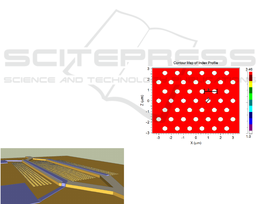
A schematic representation of the proposed device
is shown in Fig.1. The proposed MZI starts with a
single mode rib waveguide which splits into two
symmetric branches by means of an input splitter.
Hence, the two arms become parallels and are
surrounded by a proper PhC structure to increase the
propagating wave confinement in the waveguide
core. One arm acts as an optical phase shifter. To
achieve this, a transparent conductive oxide, e.g.
sputtered Al-doped ZnO (ZnO/Al) (Della Corte et al.,
2011; Rao, 2013), is deposited on the waveguide top
to apply a reverse bias to the integrated diode.
At the output, light beams interfere between each
other by means a directional coupler.
Figure 1: Schematic representation of the proposed device.
Dimensions are not in scale.
2 PHOTONIC CRYSTAL
WAVEG U ID ES DE SI G N
For the following analysis, a 2D PhC forming a
hexagonal lattice of air rods in an a-Si:H background
layer will be considered. It is known that the
hexagonal lattice pattern of a PhCW provides the
largest band gap among all PhCW geometries
allowing to obtain guiding structures which are single
mode (SM) and polarization independent (PI) at the
wavelength of 1.55 μm (Chen et al., 2009). Moreover,
a single-line defect waveguide (SLDW), created by
removing a full row of “cylinders”, leads to photonic
band gaps (PBGs) where the propagating
electromagnetic modes are forbidden inside the
structure. In order to obtain a PhC geometry with a
complete gap (Mekis et al., 1996) and PI (TE and
TM), the two materials, in this case air and a-Si:H,
should have a high refractive index contrast.
In Fig. 2 we report a generic schematic PhC
structure, with hexagonal lattice pattern, in which the
circular rods are filled with air. The bulk refractive
index was measured in our previous work and used
for the realization of a MZI EO modulator (Zelikson
et al., 1996; Della Corte 2011 et al.; Rao et al., 2013)
(n
a-Si:H
=3.46).
Figure 2: Schematic PhC structure, with hexagonal lattice
pattern, and corresponding refractive index colour bar.
In our geometry, the r and a indicate the rod radius
and lattice constant, respectively. The lattice constant
was set to 1 μm and subsequently the rod radius
varied from 0.1 μm to 0.6 μm in order to find out the
optimum value resulting in the widest band-gap for
both TE and TM modes. The results of parametric
simulation are shown in Fig. 3.
Design of Amorphous Silicon Photonic Crystal-based M-Z Modulator Operating at 1.55 µm
165
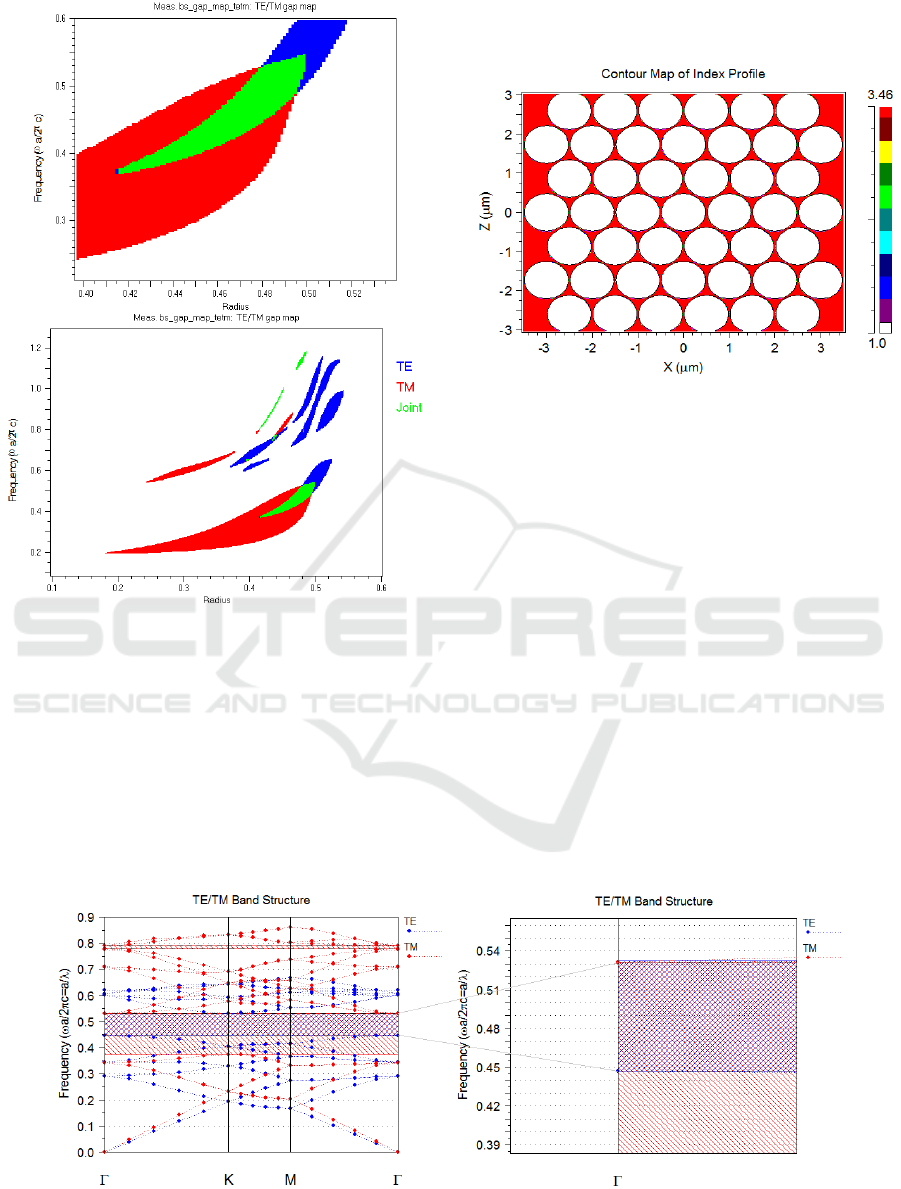
Figure 3: Gap map for the hexagonal lattice PhC.
The photonic bandgap map shown in Fig. 3
introduces red, blue and green marked areas where
the TE, TM and both of those modes are not allowed
to propagate, respectively. The rod radius values
forbidding the propagation of both TE and TM modes
(green area) can be seen in detail in the up side of
Fig.3.
A rod radius of 0.48 μm provides the widest band
gap for our structure presented in Fig.2.
In Fig. 4, the resulting PhC structure is reported
together with its refractive index.
Figure 4: PhC structure, with hexagonal lattice pattern, and
corresponding refractive index colour bar.
Subsequently, the PhC structure presented in
Fig.4 is simulated through BandSOLVE [17] tool in
order to obtain the a/λ ratio and, therefore, the
forbidden wavelength range for an optical signal
propagating through the PhC. The simulation output
is reported in Fig. 5.
Fig. 5 reveals that the simulated PhC structure
does not allow the propagation of both TE and TM
modes for the hashed area where the a/λ ratio lies
between 0.448 to 0.530.
The achieved a/λ ratio values have been also
verified through the Fullwave [17] tool by analyzing
the stop band range for both TE and TM modes, as
reported in Fig. 6, where the red circles highlight the
normalized frequency ranges at which both TE (up)
and TM (down) modes cannot propagate.
By considering the a/λ ratio varying between
0.448 and 0.53, the forbidden wavelength area is
Figure 5: Photonic band structure for both TE and TM modes.
PHOTOPTICS 2016 - 4th International Conference on Photonics, Optics and Laser Technology
166

Figure 6: Stop band ranges. The red circles highlight the
normalized frequency ranges for TE (up) and TM (down)
modes.
calculated by the product of a/λ and r/a (0.48). The
resulting forbidden wavelength area for both TE and
TM modes covers the wavelengths between 1886 nm
and 2232 nm, out of around 1550 nm.
However, for the designed geometry, as shown in
Fig. 7, a very thin diaphragm (Delta=40 nm) between
two adjacent rods has been obtained, implying
consequently a careful and expensive process for the
fabrication of the PhC-based active device.
Figure 7: Air rods. “Delta” is the distance between two
adjacent rods.
To fully exploit the advantage of the refractive
index tunability of a-Si:H by changing the PECVD
process parameters (Cocorullo et al., 1996; Rao et al.,
2012), parametric simulations have been performed
starting from different values of the a-Si:H refractive
index in order to investigate if more “relaxed”, low
cost structures, i.e., less dependent on the fabrication
tolerances and technological constraints, could be
realized. Moreover, the other goal of the parametric
simulations is to evaluate if the resulting structures
exhibit polarization dependency.
Polarization dependency and the corresponding
forbidden wavelength area of various structures are
listed in Table 1.
From Table 1, it can be seen that for an a-Si:H
with refractive index n=3.58 (already measured as
reported in Ref. (Rao et al., 2010; Rao et al., 2014;
Rao et al., 2010; Rao et al., 2010; Rao et al., 2010;
Rao et al. 2012; Rao et al., 2012)) the spacing Delta
is increased by a factor of five with respect to the
value considered in the first simulation. Due to its
simple fabrication process and calculated forbidden
wavelength area, the PhC structure - radius r=0.4 μm,
lattice constant a =1 μm – has been chosen to
integrate in the MZI structure. The photonic bands of
such structure are shown in Fig.8.
Table 1: Parametric simulation results for different refractive index values.
n a[µm] r[µm] Delta[nm] TE TM λ
min
[µm] λ
max[
µm]
3.46 1 0.48 40 Yes Yes 1886 2232
3.46 0.76 0.36 40 Yes Yes 1496 1715
3.46 0.59 0.25 90 Yes Yes 1512 1573
3.46 0.47 0.18 110 No Yes 1245 1993
3.52 1 0.39 220 Yes No 1511 1586
3.58 1 0.4 200 Yes Yes 1531 1565
Design of Amorphous Silicon Photonic Crystal-based M-Z Modulator Operating at 1.55 µm
167
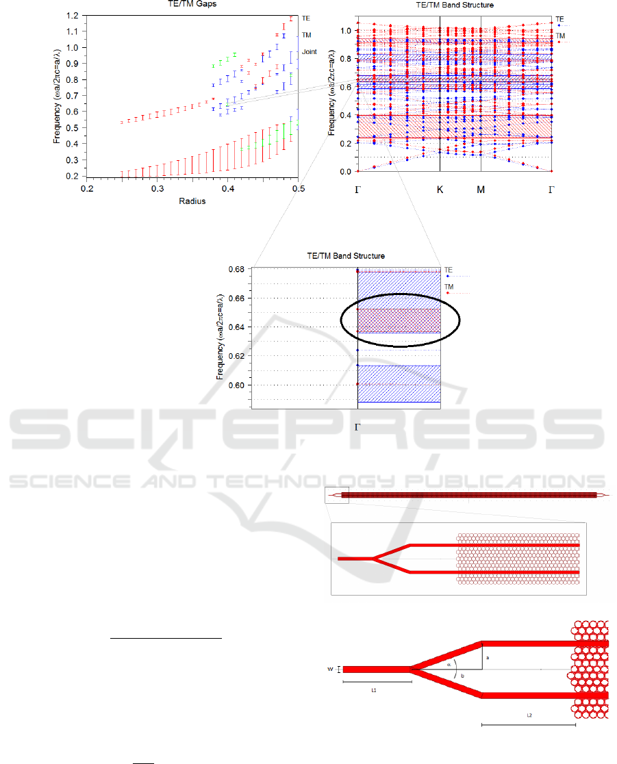
Figure 8: Photonic band structure for both TE and TM modes.
3 PHC MZI DESIGN
AND SIMULATION RESULTS
The designed PhCW has been integrated inside a MZI
in order to evaluate the phase shift, ΔΦ, induced in
the active arm by monitoring the output intensity,
which is given by (Chen et al., 2009):
where I
in
and I
out
are the MZI input and output
light beam intensities, respectively.
One can further derive the effective index change
Δneff of the waveguide mode using the equation:
where L is the active length of the phase shifter,
and λ is the wavelength in the free space. A schematic
of the PhCW structure, for Δn
eff
estimation, is
depicted in Fig. 9.
Figure 9: Schematic structure of the PhCW integrated
inside a MZI.
Parametric simulations were performed to
calculate the optimum values of the overall geometric
parameters reported in Fig. 9. In particular the
intersecting angle
α
for the input and output MZI
2
)cos(
φ
Δ⋅+
=
inin
out
II
I
Ln
eff
Δ=Δ
λ
π
φ
2
PHOTOPTICS 2016 - 4th International Conference on Photonics, Optics and Laser Technology
168
splitter has been determined in order to achieve a
trade-off between the need for a compact device and
low insertion losses. The device geometries have
been optimized in order to achieve birefringence-free,
SM propagation and acceptable coupling losses to
standard SM fibers with cleaved termination.
Simulation results are well summarized in the
following table:
Table 2: Parametric simulation results. The reported device
geometries have been optimized in order to achieve
birefringence-free, SM propagation and low coupling
losses.
W
[μm]
L1
[μm]
a [μm] b [μm]
α
[°]
L2
[μm]
1 100 4 573 0.8 100
Moreover, the impact of the refractive index
change induced in only one arm of the MZI
(surrounded by the PhC structure) was investigated
for different lengths. We designed, in fact, MZIs with
arm lengths of L=0.5 mm, 1 mm and 1.5 mm.
As already mentioned, the refractive index change
can be induced through the free carrier dispersion
effect and therefore it is controlled by the carrier
concentration profile. By reverse biasing the device,
we can induce a modulation of the space charge
volume that, in turn, modifies the refractive index
profile of the waveguide and therefore the optical
phase of the 1.55 μm wavelength light passing
through it (Zelikson, 1992).
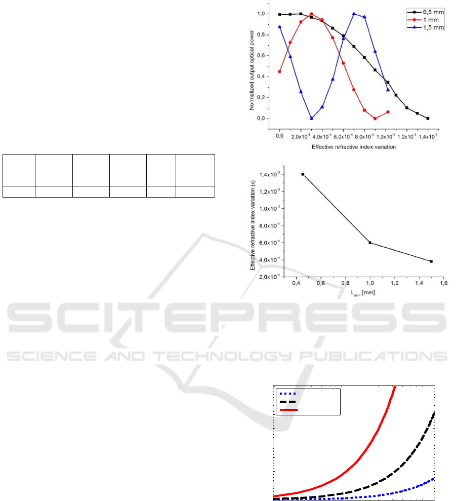
Fig. 10 (a) shows the normalized optical signal at
the MZI output as a function of the effective
refractive index change (Δn
eff
) induced in MZI arms
of different lengths, while Fig. 10 (b) reports the
effective refractive index variation required to induce
a phase shift of ΔΦ=π, between the two optical
beams, for arms of different lengths.
By using the same Δn/ΔV calculated and
experimentally measured for the a-Si:H MZI reported
in our previous work (Zelikson et al., 1992),
characterized by an arm length of 13 mm, we can
conclude that with the newly designed PhC-based
device we can obtain a full π-shift in a 1.5 mm-long
arm by applying the same driving signal (~30V), with
a consequent reduction of the V
π
×L FoM from 40
V×cm to 4.5 V×cm.
It should be finally considered that a thinning of
the waveguide core can allow a further reduction of
the driving signal amplitude necessary for a π-shift,
as the bias to drive in full depletion a p-i-n device
scales with a square law of the thickness of the
intrinsic region, as reported in Fig. 11.
(a)
(b)
Figure 10: (a) Normalized transmitted MZI optical power
vs. effective refractive index variation (Δneff) and (b)
effective refractive index variation (Δneff(π)) for inducing
a phase shift of ΔΦ=π for the three considered MZI arm-
lengths.
Figure 11: Calculated full depletion bias of a p-i-n
waveguide as a function the i-layer doping. The three
curves refer to different i-layer thicknesses (Della Corte et
al., 2011).
The proposed device, therefore, can even work
with lower driving voltage allowing a FoM as low as
of that observed in performing electro-optical
modulators in silicon (Reed et al., 2010).
10
12
10
13
10
14
0
5
10
15
20
25
30
35
40
a-Si doping concentration [cm-3]
Full-depletion bias [V]
t = 500 nm
t = 1000 nm
t = 2000 nm
Design of Amorphous Silicon Photonic Crystal-based M-Z Modulator Operating at 1.55 µm
169

4 CONCLUSIONS
In this work, numerical simulations of a PhC MZ
modulator based on a-Si:H and working at 1.55 µm,
are reported. Our FDTD numerical simulations show
that taking advantage from both the tunability
property of the a-Si:H physical parameters and the
strong optical beam confinement within a PhCW, a
more efficient phase shifting can be obtained in the
interferometric structure. Our results show that the
FoM is enhanced of an order of magnitude with
respect to our previously realized active device based
on the electrically induced free carrier dispersion
effect. In fact, by reverse biasing the vertical p-i-n
diode integrated into the PhCWs, 1.5 mm-long, we
achieved a reduction of the V
π
×L voltage-length from
40 to 4.5 V×cm and we predicted as much reduction
for sub-micron waveguide core thickness. Moreover,
the corresponding PhC fabrication process does not
require sophisticated technological facilities leading
therefore to a truly low cost technology.
REFERENCES
Vlasov, Y. et al., 2005. Active control of slow light on a
chip with photonic crystal waveguides. Nature,
438(7064), pp.65–69.
Reed, G. T. et al., 2010. Silicon optical modulators. Nature
Photonics 4 (8), pp.518 – 526.
Della Corte, F.G. & Rao, S., 2013. Use of amorphous
silicon for active photonic devices. IEEE Transactions
on Electron Devices, 60(5), pp.1495–1505.
Rao, S. et al., 2012. A 2.5 ns switching time Mach-Zehnder
modulator in as-deposited a-Si:H. Optics Express,
20(9), p.9351.
Zelikson, M. et al., 1992. Enhanced electro-optic effect in
amorphous hydrogenated silicon based waveguides.
Applied Physics Letters 61(14), pp.1664–6.
Zelikson, M. et al., 1996. Direct determination of the
quadratic electro-optic coefficient in an α-Si:H based
waveguide. J. Non-Cryst. Solids 198–200, pp.107–10.
Della Corte, F.G. et al. 2008. Electro-optically induced
absorption in a-Si:H/a-SiCN waveguiding multistacks.
Optics Express, 16(10), pp.7540-7550.
Rao, S. et al., 2010. Electrooptical Modulating Device
Based on a CMOS-Compatible a-Si:H/a- SiCN
Multistack Waveguide. IEEE Journal of Selected
Topics in Quantum Electronics, 16(1), pp.173–178.
Della, F.G. et al., Hydrogenated amorphous silicon multi-
SOI waveguide modulator with low voltage – length
product.
Rao, S. et al., 2014. Progress towards a high-performing a-
Si:H-based electro-optic modulator. Journal of Optics,
16(5), p.055501.
Della Corte, F.G. et al., 2011. Electro-optical modulation at
1550 nm in an as-deposited hydrogenated amorphous
silicon p-i-n waveguiding device. Optics express, 19(4),
pp.2941–2951.
Rao, S. & Della Corte, F.G., 2014. Numerical analysis of
electro-optical modulators based on the amorphous
silicon technology. Journal of Lightwave Technology,
32(13), pp.2399–2407.
Brimont, A. et al., 2011. High speed silicon electro-optical
modulators enhanced via slow light propagation. ,
19(21), pp.21986–21991.
Brimont, A. et al., 2009. Strong electro-optical modulation
enhancement in a slow wave corrugated waveguide.
Optics express, 17(11), pp.9204–9211.
Mekis, A. et al., 1996. High Transmission through Sharp
Bends in Photonic Crystal Waveguides. Physical
Review Letters, 77(18), pp.3787–3790.
Johnson, S.G. et al., 1998. Elimination of cross talk in
waveguide intersections. Opt. Lett. 23, pp.1855-1857.
RSoft Photonics CAD Layout User Guide, Rsoft Design
Group, Inc. Physical Layer Division, 200 Executive
Blvd. Ossining, NY 10562.
Cocorullo, G. et al., 1996. Amorphous silicon waveguides
and light modulators for integrated photonics realised
by low-temperature plasma enhanced chemical vapour
deposition. Optics Letters, 21(24), pp.2002-2004.
Rao, S., 2013. Hydrogenated amorphous silicon phase-
change device based on a p–i–p waveguiding
configuration. Optics & Laser Technology 53, pp.17-21.
Chen, X. et al., 2009. Electrooptically-active slow-light-
enhanced silicon slot photonic crystal waveguides.
IEEE Journal on Selected Topics in Quantum
Electronics, 15(5), pp.1506–1508.
Rao, S. et al., 2013. Electro-optical effect in hydrogenated
amorphous silicon-based waveguide-integrated p-i-p
and p-i-n configurations. Optical Engineering, 52(8),
p.087110.
Rao, S. & Della Corte, F.G., 2012. 1.55 m Silicon-Based
Reflection-Type Waveguide-Integrated Thermo-Optic
2×2 Switch. Optik - International Journal for Light and
Electron Optics, 123(5), pp.467–469.
Rao, S. et al., 2010. Electro-optically induced absorption in
α-Si:H/α-SiCN waveguiding multistacks. Journal of the
European Optical Society, 5, pp.10002.
Rao, S., &Della Corte, F.G., 2010. Electro-optical
modulating multistack device based on the CMOS-
compatible technology of amorphous silicon”, Journal
of the European Optical Society, 5, pp.10040.
Rao, S. et al., 2010. Low-loss amorphous silicon
waveguides grown by PECVD on indium tin oxide.
Journal of the European Optical Society, 5, pp.10039.
Rao, S., Della Corte, F.G. & Summonte, C., 2012.
Amorphous silicon waveguides grown by PECVD on
an Indium Tin Oxide buried contact. Optics
Communications, 285(13-14), pp.3088–3092.
Rao, S. et al., 2012. All-optical modulation in a CMOS-
compatible amorphous silicon-based device. Journal of
the European Optical Society, 7, pp.12023.
PHOTOPTICS 2016 - 4th International Conference on Photonics, Optics and Laser Technology
170
