
Laser-based Soldering Technique for Hermetical Sealing of the
Calibration Target for the Exomars’ Raman Instrument
Thomas Burkhardt
1
, Michael Seifert
1
, Pol Ribes
1,2
, Nicolas Lange
1
, Guillermo Lopez-Reyes
3
,
Andoni Moral-Inza
4
and Antonio Sansano
3
1
Fraunhofer Institute for Applied Optics and Precision Engineering IOF, Albert-Einstein-Str. 7, 07745 Jena, Germany
2
Institute of Applied Physics IAP, Friedrich-Schiller University Jena, Max-Wien-Platz 1, 07743 Jena, Germany
3
Unidad Asociada UVA-CSIC-CAB, Universidad de Valladolid, Parque Tecnológico Boecillo, 47151 Valladolid, Spain
4
Instituto Nacional del Tecnica Aerospacial INTA, Ctra Ajalvir Km4, 28850 Torrejón de Ardoz, Spain
Keywords: ExoMars Raman Laser Spectrometer, Calibration Target, Laser-based Soldering, Solderjet Bumping,
Hermetical Sealing.
Abstract: We propose the laser-based Solderjet Bumping as a full inorganic joining technique for the hermetical
sealing of a possible calibration target container for the ExoMars Raman Laser Spectrometer. This
technique allows the adhesive free bonding in a flux free and localized soldering process. We show a finite
elements analysis based optimization of a soldering adapted design for the calibration target container.
Current experimental results document hermetical sealing of a stainless steel tube with BK7 and D263
windows with a helium leakage rate down to 5·10
-6
mbar·l·s
-1
.
1 INTRODUCTION
1.1 Motivation
In 2018 ESA/Roscosmos will launch the ExoMars
Rover mission. The main target of this mission is to
study the Martian environment and to test new
technologies paving the way for a possible Mars
return mission in the 2020s. Raman spectroscopy is
a tool for the chemical and structural identification
of (sub-)surface materials and organic analysis to
address the scientific objective of the Pasteur
payload to search for evidence of past and present
life on Mars (Rull Pérez and Martinez-Frias, 2006;
Escudero et al., 2008). The Raman Laser
Spectrometer (RLS) is together with the MicrOmega
(IR spectrometer) and the Mars Organic Molecule
Analyzer (MOMA) part of the rover’s analytical
laboratory drawer (ALD). They are key exobiology
experiments on the ExoMars rover mission to
examine the chemical composition of geological
samples acquired from depths of up to two meters,
where possible organic molecules may be protected
from destructive cosmic radiation and/or oxidative
chemical reactions (Arevalo et al., 2015). For
calibration of the RLS on board the rover, a
calibration target (CT) will be included. This allows
periodic calibration of the instrument for high
precision and to evaluate the health of the system
during the mission (Sansano et al., 2014). During
each analysis (several hours), at least 20 spectra at
different points of the sample will be acquired.
Before each experiment cycle, the CT will be used
to assess the calibration status of the whole
instrument in an end-to-end calibration, including
the laser optical head, harness, spectrometer, and
electronics. There will be at least 22 experimental
cycles, each of them with a different sample.
As the CT will be located in the ultra clean zone
(UCZ) of the ALD, the CT container is to be
suitably sealed. It needs to comply with planetary
protection requirements to prevent biological
contamination of Mars to preserve its pristine nature
and also to prevent the corruption of the mission’s
experiments. To achieve this ambitious protection
and contamination control COSPAR Cat IVb
classification measures are implemented to avoid the
terrestrial contamination of the analyzed samples.
According to Richter et al. (2015) this addresses the
whole Sample Processing and Distribution
Subsystem (SPDS) and includes the pressurized
UCZ (pressurized during launch, transfer, and
landing), sterilization of the ALD sample chain, ultra
Burkhardt, T., Seifert, M., Ribes, P., Lange, N., Lopez-Reyes, G., Moral-Inza, A. and Sansano, A.
Laser-based Soldering Technique for Hermetical Sealing of the Calibration Target for the Exomars’ Raman Instrument.
DOI: 10.5220/0005653200550061
In Proceedings of the 4th International Conference on Photonics, Optics and Laser Technology (PHOTOPTICS 2016), pages 57-63
ISBN: 978-989-758-174-8
Copyright
c
2016 by SCITEPRESS – Science and Technology Publications, Lda. All rights reserved
57
cleaning of the ALD sample chain components, and
integration of the hardware in a high cleanliness
environment.
1.2 Solderjet Bumping Technique
We propose the laser-based Solderjet Bumping as a
full inorganic joining technique for the hermetical
sealing of a possible CT container candidate. It
allows the adhesive free bonding of heterogeneous
materials, e.g. metals with glass, in a flux free
process. The soldered assembly is therefore
completely free of undesired organic compounds.
Furthermore the solder joints are able to withstand
high thermal loads during sterilization and high
energetic radiation, e.g. cosmic radiation during
transfer of the lander to and its mission on Mars.
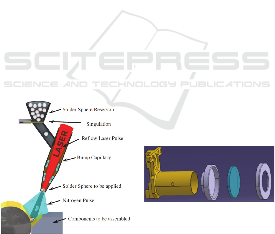
Solderjet Bumping (Figure 1) is a laser-based
soldering process that is especially well suited for
the joining of optical components made of fragile
and/or brittle materials like glasses or ceramics.
Spherical solder preforms that consist of soft solders
alloys, e.g. tin-based lead-free solders or eutectic
gold-tin, are used in a diameter range of 60 µm to
760 µm. These spheres are transferred from a
reservoir to a placement capillary next to the joining
geometry of the components to be bonded together.
After positioning, the material is molten by a fiber-
coupled, infrared laser pulse and jetted out of the
capillary. Nitrogen is used as an inert gas flow. The
liquid solder droplets account for a very good
thermal contact of the alloy with the components.
Figure 1: Solderjet Bumping operation principle (Beckert
et al., 2010).
We have demonstrated the versatility of this
technique for the high accuracy packaging of
photonic micro-systems (Beckert et al., 2010).
Hermetical sealing of biomedical devices (Beckert et
al., 2011) and the vacuum compatibility of soldered
assemblies for the use in electron beam lithography
(Burkhardt et al., 2011) have been proven. We
presented Solderjet Bumping for optical
instrumentation in aerospace applications (Burkhardt
et al., 2015). The technique has been used for the
manufacturing of a compact and robust, solid-state
laser for the ExoMars mission and was tested at
thermal and radiation (proton and gamma) loads
(Ribes et al., 2015).
2 DESIGN AND OPTIMIZATION
2.1 Requirements
The CT consists of a cylindrical, stainless steel
container of 5..6 mm diameter. A cavity in the
container will be covered by a thin glass window,
fused silica and BK7 will be discussed as candidates.
The window will contain the calibration sample and
needs therefore to be hermetically sealed to prevent
organic molecular contamination of the UCZ. A
mixture of powdered standard compounds (both
organic and inorganic) with a known spectral Raman
response covering the entire spectral range will be
filled in this sealed envelope (Sansano et al., 2014).
Regarding the calibration sample both an
encapsulated mixture – a pill with diameter 4 mm
and thickness 3 mm – and non-encapsulated powder
are discussed. The main laser characteristics during
calibration are continuous operation at 532 nm, with
50 mW optical output power that is focused on
50 µm diameter spot on the sample.
Figure 2: Design proposal of CT holder elements (Sansano
et al., 2014).
BK7 is selected over its radiation resistant
counterparts (e.g. BK7G18) for multiple reasons.
These include availability as thin glass sheets and
manufacturability to the designed shape, its
PHOTOPTICS 2016 - 4th International Conference on Photonics, Optics and Laser Technology
58
thermomechanical properties with respect to the
stainless steel receptacle. A trade-off in BK7’s
preferability for space applications in terms of
radiation damage is accepted as radiation
obscuration is well characterised for ionising and
non-ionising doses is accepted for a known Raman
signature of the material. Given that the window of
the CT container would be placed very deep inside
the ALD of the rover the expected radiation levels
should not to be a major concern for the obscuration
of the window.
Due to obvious weight restrictions the maximum
required weight is 9 g with a further decrease to 4 g
during STM (structural and thermal model) design.
Figure 2 shows the design proposal of a CT and
holder elements as a basis for the design
considerations of a CT suitable for Solderjet
Bumping. The required envelope, including the
support, is the one contained in a parallelepiped of
13×26.3× 10.9 mm³.
The thickness of the glass window is required to
be 100 µm maximum. A maximum height difference
between the top surface of the window and the
solder joint of 50 µm is permitted. This is necessary
for the CT to be within the agreed envelope for
avoiding any interference with the rover’s carrousel
powdered sample flattener.
2.2 Design and FEA Results
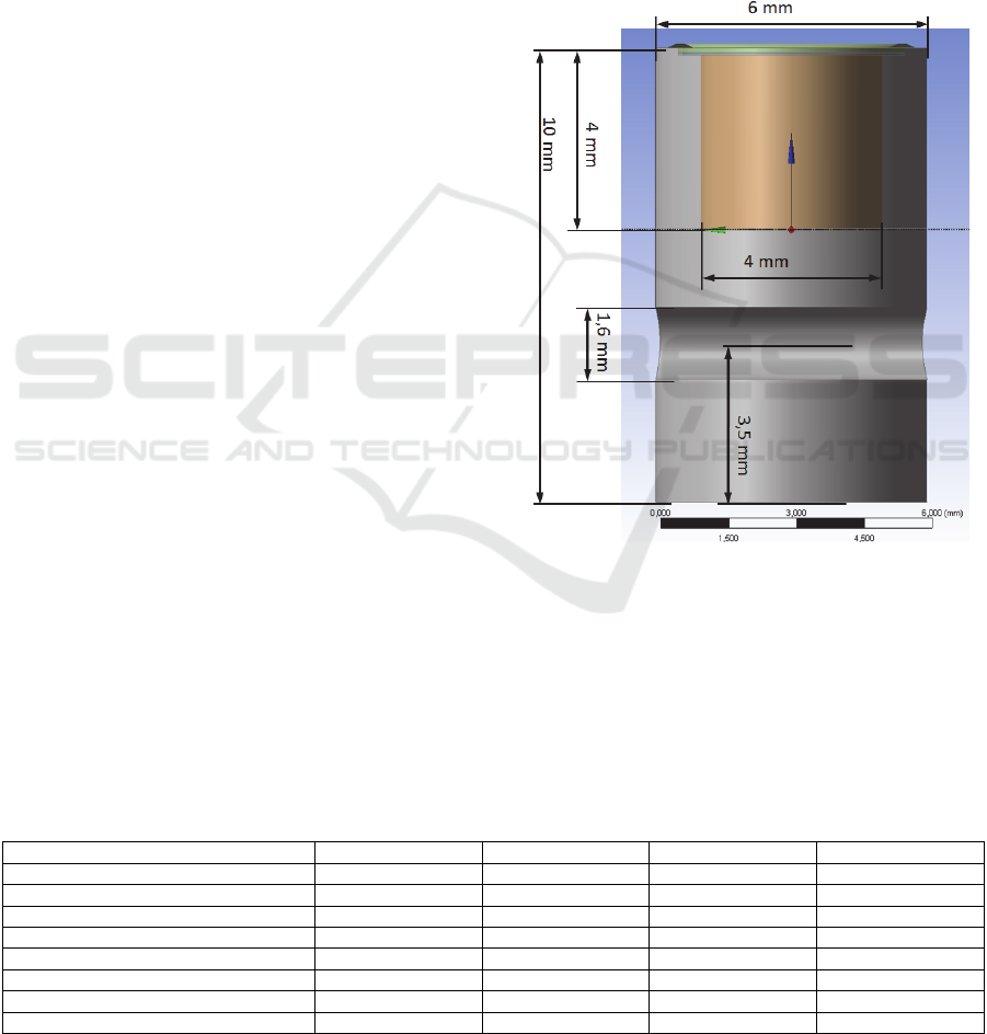
Based on the requirements of the CT a model of the
receptacle is developed to simulate and evaluate
thermomechanical, shock, acceleration, and
vibrational loads. Different solder joint geometries
are investigated and optimized according to the
results of the finite elements analysis (FEA).
Figure shows the model and initial dimensions
used in FEA simulations and optimization. The
simplified model omits the enclosed powder sample
as thermomechanical simulations will not be
affected as there is no transfer of forces or momenta.
In dynamic simulations the powder would act as an
additional mass, dampening the response behavior of
the whole receptacle thus the simulated empty
system shows the worst case results.
Details of the solder joint showing the receptacle,
the window, and the solder itself are depicted in
Figure 4. A gap of 100 µm between receptacle and
window is assumed to accommodate for
manufacturing tolerances. Initial simulations
assumed the shown 600 µm width and 100 µm
height of the solder joint to bridge this gap. These
values could be achieved using a solder sphere
diameter of 400 µm, overlapping placement, and
typical, experimentally validated wetting behavior.
Figure 3: Simulated receptacle with dimensions.
Material parameters used for the simulations for
the stainless steel, the window (both fused silica and
BK7), and the solder alloy (SAC305 = Sn3Ag0.5Cu)
are listed in Table 1. The equivalent Von-Mises
stresses as well as the total deformation are
evaluated in all three individual parts: receptacle,
glass window, and solder ring.
Table 1: Material parameters used for FEA simulations.
Stainless Steel Fused Silica BK7 SAC305
Young’s Modulus / GPa 193 73.2 82 44
Poisson’s Ratio 0.31 0.17 0.21 0.36
Density 7.75 2.02 2.2 7.4
CTE / 10
-6
·K
-1
17 0.56 7.1 22.4
Thermal Conductivity / W·m
-1
·K
-1
15.1 1.4 1.1 56.3
Specific Heat / J·kg
-1
·K
-1
480 750 858 283
Yield Strength / MPa 207 N/A N/A N/A
Ultimate Tensile Strength / MPa 586 50 63.5 45
Laser-based Soldering Technique for Hermetical Sealing of the Calibration Target for the Exomars’ Raman Instrument
59
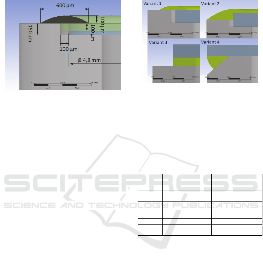
Figure 4: Detail of the solder joint of the receptacle with
initial design values.
2.3 Design Optimization
2.3.1 First Iteration
First thermomechanical simulations according to the
model presented in Figure 3 and Figure 4 and a
temperature range from -60 °C to +130 °C show
maximum stresses in the solder of 229 MPa and in
the window (fused silica) of 133 MPa. Both
significantly exceed the ultimate tensile strength
(UTS) of these materials (see Table 1) which is
mainly caused by the large mismatch of the
coefficient of thermal expansion. Static structural
acceleration, transient structural shock, harmonic
load, and random vibration simulation all show
acceptable stress levels with a minimum safety
factor of 8.5. The results are not presented here as
the model had to be refined to improve the thermal
behavior.
To avoid damage to the solder and window a
design optimization is investigated. Besides a
reduction in differential thermal expansion (DTE) a
few concepts are followed and simulated
accordingly. A promising approach is a changed gap
between the components, a thicker glass material, a
cylindrical geometry with reduced stiffness at the
top of the receptacle, and a change in geometry of
the solder joint.
A refined geometry with reduced stiffness at the
top of the receptacle minimizing DTE to relief stress
uses a reduced wall thickness of the cylinder of
0.5 mm compared to initial 1 mm. The gap between
cylinder wall and window is decreased – a measure
that requires tighter tolerances for the experimental
samples. Furthermore the solder joint size is
decreased both in width and thickness, which will
experimentally be realized by using smaller solder
spheres (diameter 100 µm or 150 µm).
Figure 5: Refined geometries of iteration 1.
In addition to the changed geometry the
simulations were done with Fused Silica as well as
BK7 as glass material. The advantage is the
significantly increased CTE of BK7, lowering the
DTE with respect to the steel tube, and the increased
UTS compared to Fused Silica (see Table 1). Four
geometries are investigated as shown in
Figure.
Table 2: Maximum Von-Mises stresses in solder joint and
glass window for thermal load of 130 °C and calculated
minimum safety factors (FS denotes Fused Silica).
Type
Solder
Stress /
MPa
Solder
Safety
Factor
Window
Stress /
MPa
Window
Safety
Factor
V1, FS 378 0.12 240 0.21
V1, BK7 232 0.19 162 0.39
V2, FS 381 0.12 155 0.32
V2, BK7 258 0.18 109 0.58
V3, FS 209 0.22 158 0.32
V3, BK7 138 0.33 109 0.58
V4, FS 1380 0.03 269 0.19
V4, BK7 881 0.05 183 0.35
Table 2 lists the resulting maximum Von-Mises
stresses for a thermal load of 130 °C and the
respective minimum safety factors using UTS values
as listed in Table 1. While the stresses in the solder
and the glass window still significantly exceed the
materials UTS an improvement due to the use of
BK7 can be observed. This is traced back to the CTE
which is 12 times higher for BK7 than for Fused
Silica and the 13.5 MPa higher UTS. Variants 1, 2,
and 4 show stress distributions with very localized
peaking that indicate a potential improvement by
refining the geometry.
2.3.2 Second Iteration
Based on the results for the four variants discussed
in the previous sub subsection, the geometries for
three variants are further refined and simulated again
under the same conditions. Due to overall low
PHOTOPTICS 2016 - 4th International Conference on Photonics, Optics and Laser Technology
60
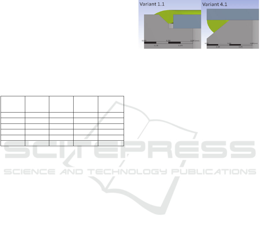
stresses variant 2 will not be refined further.
Variants 1, 3 and 4 on the other hand are showing
potential for further improvements and are therefore
further investigated. In addition plasticity of the
solder alloy is added to the model to create a more
realistic representation. Figure 6 shows the improved
geometries 1.1 and 4.1 with rounded edges to
minimize stress. Variant 3.1 is similar to variant 3 as
depicted in Figure 5 with a decreased solder layer
thickness of 50 µm. Table 3 lists the maximum Von-
Mises stresses for a thermal load of 130 °C
respective minimum safety factors using UTS values
as listed in Table 1 for the improved designs both for
elastic and plastic modelling of the solder.
Table 3: Maximum Von-Mises stresses in solder joint and
glass window for thermal load of 130 °C and calculated
minimum safety factors for second design iteration.
Calculations using plasticity are marked with an asterisk.
Type
Solder
Stress /
MPa
Solder
Safety
Factor
Window
Stress /
MPa
Window
Safety
Factor
V1.1 238 0.2 101 0.6
V1.1 * 51 0.9 75 0.8
V3.1 163 0.3 110 0.6
V3.1 * 48 0.9 85 0.8
V4.1 259 0.2 167 0.4
V4.1 * 52 0.9 113 0.6
The plasticity allows the solder alloy to balance
and even out the occurring stresses in the
components, thus increasing the minimum stresses
but decreasing the maximum stresses. As a result the
minimum safety factors increase and the maximum
safety factors decrease (note that only minimum
safety factors are listed in Table 3). Considering
these changed stress and safety factor conditions,
variant 1.1 (as calculated with plasticity) shows the
optimal compromise of a sufficiently high minimum
and maximum safety factor in all three components.
In addition variant 1.1 has the best prerequisites for
the technological realization in contrast to the more
complicated solder process required for variant 3.1
and 4.1. With refining the geometries of the three
chosen variants the occurring stresses could be
further reduced. By introducing the plasticity to
material formulation of the solder alloy said stresses
were successfully smoothed and balanced in all three
components, reducing the extreme values.
All evaluations were done with the absolute
maximum stress values that occur at each
component representing the worst case. The average
stress in each component is expected to be
significantly lower and indicates the possible use of
soldering the proposed assemblies. Transient and
dynamic mechanical load cases were simulated for
the optimized models and show minimum safety
factors of 14.5 and a first Eigenfrequency of 50 kHz.
Considering these mechanical loads an assembly of
the CT using Solderjet Bumping seems feasible.
Figure 6: Refined geometries of iteration 2.
3 EXPERIMENTAL RESULTS
As suggested by the results variants 1 and 1.1 are the
most promising candidates for successful soldering.
Furthermore variants 3.x and 4.x require
significantly more elaborate handling equipment.
Experimental verification as reported in this paper is
therefore using samples made according to design
variants 1 and 1.1.
Due to commercial availability one batch of
experiments was conducted using D263 glass which
shows similar thermomechanical properties as BK7
especially an equivalent CTE but is available as thin
sheet glass (thickness 145 µm). These samples were
prepared at IOF from sheets. The second batch of
experiments was done using BK7 windows with a
thickness of 175 µm. These samples were also
prepared at IOF from sheets. A third batch of BK7
samples was procured from Laser Optex, China,
with a thickness of 150 µm ± 2 µm.
Both the windows and the stainless steel cylinder
are covered by a solderable thin film metallization. It
is provided by physical vapor deposition and
consists of three layers: titanium, platinum, and
gold. The metallization system has an overall
thickness of approx. 500 nm. Titanium acts as
adhesion promoter, platinum as diffusion barrier,
and the wettable, non-oxidizing gold finish supports
the required flux-free processing to achieve a clean
solder joint. (Banse et al., 2005) reported this system
among others as a suitable and well adhering
metallization for glass materials.
3.1 Soldering and Optical Inspection
Soldering is conducted using a solder sphere
diameter of 100 µm and 150 µm according to the
optimized design of the solder joints. Relevant
Laser-based Soldering Technique for Hermetical Sealing of the Calibration Target for the Exomars’ Raman Instrument
61
parameters for the laser-based Solderjet Bumping
are the reflow energy governed by laser pulse width
and laser current. Using glass slides these parameter
sets are evaluated to find proper wetting of the
solder in the substrate while preventing damage to
the glass. The latter is especially an issue with
soldering as thermal shock can cause cracks to form
and propagate in the glass leading to failures of the
bond. We found suitable parameters as listed in
Table 4. The increased necessary energy
corresponds well to increased solder volume and
mass (approx. factor 3.4). These investigations show
the limited parameter space for soldering thin sheet
glass and the possible issues with soldering near the
edges of said glass sheets.
Table 4: Laser reflow parameter sets.
Solder
Sphere
Diameter /
µm
Laser
Current /
mA
Laser Pulse
Width /
ms
Puls Energy
/
mJ
100 1500 1 7.4
150 1700 2.4 22.5
Glass windows are inserted in the stainless steel
tube, adjusted for an even and symmetrical
distribution of the gap around the circumference,
and kept in place by application of vacuum. A bond
height – the distance of the Solderjet’s placement
capillary to the soldered components – of 350 µm
for 100 µm solder spheres and 550 µm for 150 µm is
used. These distances are selected to provide
undisturbed application of the liquid solder droplet
with minimized deviation of placement accuracy.
Soldering is a sequential process to subsequently
place multiple overlapping bumps. We investigated
different placement strategies, e.g. an interlaced
placement scheme and multiple turns to
accommodate for a larger gap between window and
tube due to issues with tolerances. We did not find a
significant influence of the placement scheme on
leakage rate as long as a completely closed solder
joint is achieved and no holes are observable by
visual inspection. Placement of solder droplets is
done in an automated system using a vision system
and a circular fit to adjust the machine’s tool path
with the outline of the sample. A total of 288 bumps
per turn are placed at a solder sphere diameter of
100 µm and 232 bumps per turn for 150 µm preform
diameter, respectively.
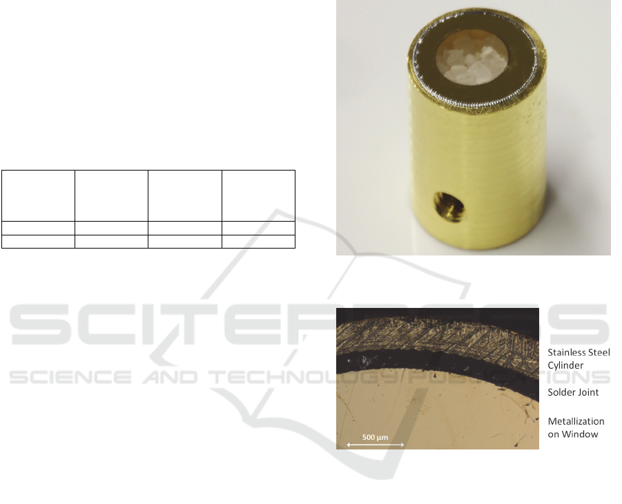
Figure 7 shows a sealed CT filled with mock-up
sample compound. The total weight of the sample is
less than 2 g within the STM design limit. A total
height of the solder joint of less than 50 µm is
achieved using solder droplet diameters of 100 µm.
Figure 8 shows a top view photomicrograph of the
sample and the solder joint. It illustrates clearly the
regular and clean overlapping placement of multiple
solder droplets in the bond zone to provide proper
mechanical fixation of the window as well as
hermetical sealing.
Figure 7: Sealed calibration target filled with mock-up
sample compounds and BK7 window.
Figure 8: Photomicrograph of solder joint.
3.2 Helium Leakage Testing
For measuring the leakage rate a Leybold Inficon
UL200 was used. Minimum detectable leakage rate
in vacuum mode is 5·10
-11
mbar·l·s
-1
. For testing, the
cylinders were fixed with an adapter to the leak
tester and evacuated. The soldered windows were
then sprayed with Helium and the leakage rate was
measured.
For batch one using D263 glass, thickness
145 µm, out of seven samples we found one sample
exceeding 5·10
-6
mbar·l·s
-1
, three samples exceeding
10
-4
mbar·l·s
-1
, and one sample exceeding 10
-2
mbar·l·s
-1
.
With BK7 glass, thicknesses of 175 µm and
150 µm, out of eight samples we found two samples
exceeding 10
-4
mbar·l·s
-1
, two samples exceeding
PHOTOPTICS 2016 - 4th International Conference on Photonics, Optics and Laser Technology
62

10
-3
mbar·l·s
-1
, and three sample exceeding 10
-2
mbar·l·s
-1
. A major issue is the surface quality of the
window’s edges. We observe the formation of
micro-cracks during soldering which in turn
significantly increase leakage rate. While the
procured windows show a very narrow thickness
tolerance, the edges are not polished and therefore
susceptible to crack induced by thermal shock.
4 CONCLUSIONS
We have shown the hermetical sealing of a multi-
material assembly for the possible use as a
calibration target container for the ExoMars Raman
Laser Spectrometer. Proof-of-concept samples made
of stainless steel and D263 achieved leakage rates of
5·10
-6
mbar·l·s
-1
. The bonding is completely
inorganic and therefore suitable for high cleanliness
and contamination free applications, e.g. under
COSPAR planetary protection requirements.
A FEA tool chain and models were set up for
optimization of joint geometries and were used to
provide appropriate design recommendations for
minimized stresses. Mechanical and
thermomechanical load cases were investigated by
numerical simulations. A minimized differential
thermal expansion is found to be necessary to
achieve acceptable stress levels in the solder joint.
Although the presented design of the container
and therefore the proposed bonding will not be used
for the RLS CT the results show the adequacy of
Solderjet Bumping for hermetical sealing and
aerospace applications. The development activities
continue and the technology is kept as a backup plan
for the ExoMars RLS CT.
Further improvements of leakage rate and
reduced failures during bonding are expected with
optimized sample geometries, improved surface
quality of the windows’ circumferential side faces,
and adapted tolerances between receptacle and
window. A goal would be to achieve a helium
leakage rate better than 10
-8
mbar·l·s
-1
. Experimental
qualifications based the mechanical and thermal load
cases considered for the numerical optimizations
have to be conducted with further samples.
ACKNOWLEDGEMENTS
The authors gratefully acknowledge funding from
MINECO, Spain, through project ESP2013-48427-
C3-2-R.
REFERENCES
Arevalo, R., Brinckerhoff, W., van Amerom, F., Danell,
R., Pinnick, V., Xiang Li, Getty, S., Hovmand, L.,
Grubisic, A., Mahaffy, P., Goesmann, F., Steininger,
H., 2015, Design and demonstration of the Mars
Organic Molecule Analyzer (MOMA) on the ExoMars
2018 rover, in: Aerospace Conference, 2015 IEEE.
Banse, H., Beckert, E., Eberhardt, R., Stöckl, W., Vogel,
J., Laserbeam soldering– a new assembly technology
for micro optical systems, Microsyst. Technol. 11,
186–193 (2005).
Beckert, E., Burkhardt, T., Hornaff, M., Kamm, A.,
Scheidig, I., Stiehl, C., Eberhardt, R., Tünnermann, A.,
2010, Submicron accuracy optimization for laser beam
soldering processes, Proc. SPIE 7585, 758505.
Beckert, E., Wippermann, F., Walther, S., Burkhardt, T.,
Messerschmidt, B., Bartnitzek, T., Vahrenkamp, T.,
Eberhardt, R., Gäbler, D., Tünnermann, A., 2011,
Autoclaveable miniaturized video endoscopes with
simplified flip-chip assembly, Proc. SPIE 7893,
78930B.
Burkhardt, T., Mohaupt, M., Hornaff, M., Zaage, B.,
Beckert, E., Döring, H.-J., Slodowski, M., Reimer, K.,
Witt, M., Eberhardt, R., Tünnermann, A., 2011,
Packaging Technology of Multi Deflection Arrays for
Multi-Shaped Beam Lithography, Proc. of IMAPS 44
th
International Symposium on Microelectronics.
Burkhardt, T., Hornaff, M., Kamm, A., Burkhardt, D.,
Schmidt, E., Beckert, E., Eberhardt, R., Tünnermann,
A., 2015, Low-strain laser-based solder joining of
mounted lenses, Proc. SPIE 9574, 9574-21.
Escudero-Sanz, I., Ahlers, B., Bazalgette Courrèges-
Lacoste, G., 2008, Optical design of a combined
raman–laser-induced-breakdown-spectroscopy
instrument for the european space agency exomars
mission, Opt. Eng., vol. 47, no. 3, pp. 033001-1–
03301-11 .
Ribes, P., Burkhardt, T., Hornaff, M., Kousar, S.,
Burkhardt, D., Beckert, E., Gilaberte, M., Guilhot, D.,
Montes, D., Galan, M., Ferrando, S., Laudisio, M.,
Belenguer, T., Ibarmia, S., Gallego, P., Rodriguez, J.
A., Eberhardt, R., Tünnermann, A., 2015, Solderjet
bumping technique used to manufacture a compact
and robust green solid-state laser, Proc. SPIE 9520,
952009.
Richter, L., Carianni, P., Durrant, S., Hofmann, P.,
Mühlbauer, Q., Musso, F., Paul, R., Redlich, D., 2015,
Progress Report on Development of the Exomars 2018
Sample Processing and Distribution Subsystem
(SPDS) and related OHB Sample Handling Studies,
Astra 2015 ESTEC.
Rull Pérez, F., Martinez-Frias, J., 2006, Raman
spectroscopy goes to Mars, Spectroscopy Europe, vol.
18, pp. 18–21.
Sansano, A., Navarro, R, Lopez-Reyes, G., Rull, F., 2014,
Development of the Calibration Target for ExoMars’
Raman Instrument (RLS), 45
th
Lunar and Planetary
Science Conference.
Laser-based Soldering Technique for Hermetical Sealing of the Calibration Target for the Exomars’ Raman Instrument
63
