
DPA Resistance Enhancement through a Self-healing PLL based
Power Mask
Fleura Hajilou, Ehsan Mazidi and Shahab Ardalan
Center for Analog and Mixed Signal, San Jose State University, 1 Washington Sq, San Jose, CA, U.S.A.
Keywords: Side Channel Attack, DPA, Masking, Power Masking.
Abstract: Attackers can benefit from different side-channel properties such as timing information, electromagnetic
leaks and power consumption to achieve private key of a crypto-processor. Among side channel attacks,
Differential Power Analysis (DPA) is widely used by hackers. In this paper a new approach is presented to
make a system more immune to DPA. The proposed technique employs a low power Phase Locked Loop
(PLL) to isolate supply voltage from crypto processor. The proposed method is implemented in 45nm
CMOS technology.
1 INTRODUCTION
Today smart cards play an important role in
everyday life. Hundreds of millions of smart cards
are used today in variety of applications which
contain sensitive data and private information. Since
exposure of information on device could have
serious consequences, privacy and protection of the
data is a crucial task. Different encryption
techniques are introduced to keep the data out of the
hands of hackers. Since all attacks take the
advantage of change in processing behavior, the
primary approach for securing data is to mask these
changes from hackers. Among all side channel
attacks, power analysis is more popular to use
because it is easy to implement and hard to avoid
(Shamir, 2000). This technique noninvasively
extracts information from power consumption of a
cryptographic hardware device. There are two
categories of power analysis for side channel
attacks: Simple Power Analysis (SPA) and
Differential Power Analysis (DPA). There are
several reported studies to make a system more
immune to power analysis attacks (Tiri et al., 2002),
(Li et al., 2007), (Zadeh et al., 2011) and (Toprak
and Leblebici, 2005) which are discussed briefly in
this paper. The organization of the paper is as
follows:
In section 2 a brief introduction to SPA and DPA
and different approaches of countermeasure is
presented. Section 3 discusses about PLL operation
and the way it de-correlates the crypto-processor
from monitored power line. In section 4 design
considerations of PLL based technique is explained.
Simulation results are shown in section 5.
Conclusion is presented in section 6.
2 SPA, DPA AND DIFFERENT
APPROACHES OF
COUNTERMEASURE
Integrated circuits are built out of individual
transistors which act as voltage controlled switches.
Current flows across transistor substrate when
charge is applied to (or removed from) the gate. This
current then delivers charge to the gates of other
transistors, inter connect wires and other circuit
loads. The motion of electric charge consumes
power and produces electromagnetic radiation, both
of which are externally detectable. The first step in
power analysis process is to collect one or more
traces from the target device. A trace is a sequence
of measurements taken across a cryptographic
operation or sequence of operations (Cocher et al.,
1999). Simple Power Analysis (SPA) is a method
that directly monitors power consumption of the
hardware in order to detect individual bits of public
key. SPA is only effective if operations are
dependent on key bits. On the other hand
Differential Power Analysis (DPA) is based on
statistical analysis of power consumption during a
certain amount of time. DPA attacks measure power
levels at different parts of the chip and apply
267
Hajilou F., Mazidi E. and Ardalan S..
DPA Resistance Enhancement through a Self-healing PLL based Power Mask.
DOI: 10.5220/0005547302670272
In Proceedings of the 12th International Conference on Security and Cryptography (SECRYPT-2015), pages 267-272
ISBN: 978-989-758-117-5
Copyright
c
2015 SCITEPRESS (Science and Technology Publications, Lda.)
statistical analysis to overcome countermeasures
such as noise. Evaluating power consumption
reveals the type of operation that is being done. An
analysis performed by hacker specifies bits of the
crypto key. The process is repeated to eventually
produce the entire key. The DPA attack is more
effective than SPA and is useful when individual
bits of secret key cannot be detected due to error and
environmental noise.
To countermeasure DPA there are both software
and hardware solutions. Reducing signal sizes and
attenuating noise to make reduced signal sizes easier
to detect (Messerges et al., 2002) are some of the
early works done to countermeasure DPA. Today to
resist DPA attacks, hiding and masking methods are
commonly used. With the power masking
correlation becomes very weak because this allows
the power consumption of the IC to be independent
from the algorithm operation. To make a system
more immune to DPA attacks one solution is to
implement items in a logic family that combines
differential and dynamic logic. Sense Amplifier
Based Logic (SABL) (Tiri et al., 2002), Dynamic
Current Mode Logic (DCML) (Li et al., 2007),
Current-Balanced Logic (CBL) (Zadeh et al., 2011)
and current mode circuits (Toprak and Leblebici,
2005) are examples of this method. However these
modified logics usually result in high area overhead
and cost.
Another approach attempts to isolate power
supply from the crypto-processor block. Employing
some kind of hardware methods (Corsonello et al.,
2006), switch capacitor current equalizers
(Tokunaga and Blaauw, 2010) and switched
capacitor techniques (Shamir, 2000) are examples of
such an approach. This paper presents a novel power
supply isolation technique by employing a phase
locked loop to de-correlate power supply from the
crypto-processor block.
3 PHASE LOCKED LOOP AND
POWER SUPPLY ISOLATION
A PLL is a feedback system that generates an output
signal whose phase is proportional to the phase of
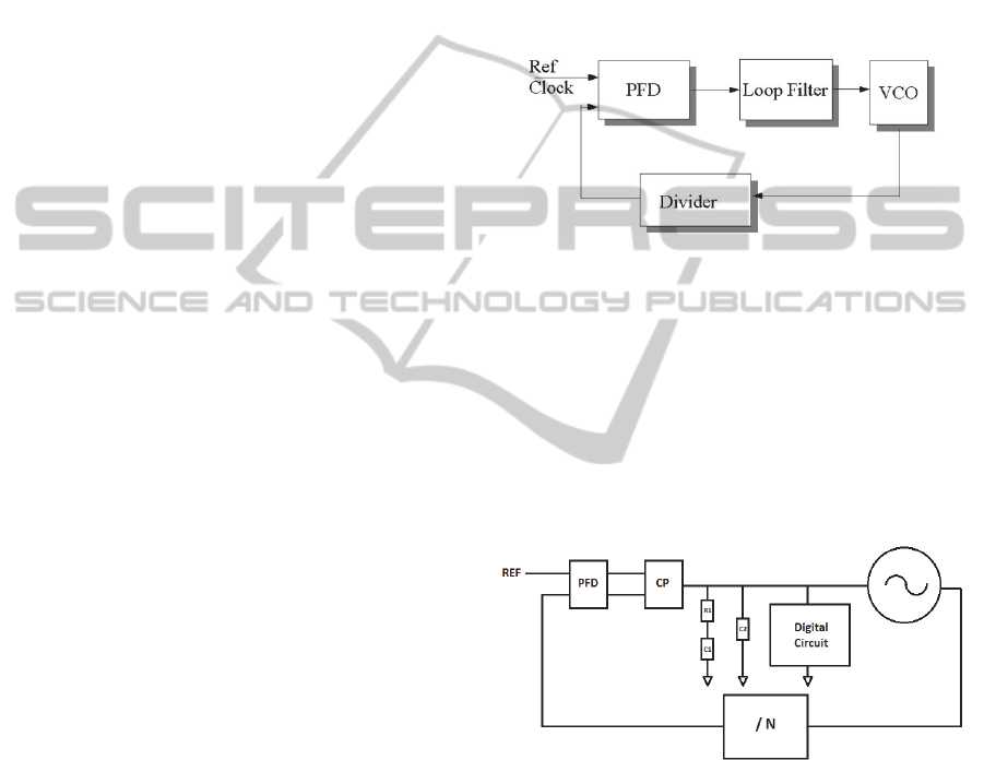
the reference signal applied to the input (Figure1).
PLLs are widely used in wireless/wireline
communication as well as clock generators in
processors. There are four basic blocks in a PLL:
1. PFD: Phase Frequency Detector is a circuit that
detects both frequency and phase mismatch
between the reference and the feedback signals.
Depending on the type of the PFD, it can be a
pulse of current or voltage.
2. LF: Loop Filter makes the system stable and
removes high frequency components of the PFD
output. In locked condition, the output of LF is a
constant dc voltage.
3. VCO: Voltage Controlled Oscillator generates a
periodic output whose frequency is proportional
to the input dc voltage.
4. Divider: It divides the output phase and enables
us to have different output frequencies.
Figure 1: PLL Building Blocks.
The control voltage of VCO determines the
instantaneous frequency of oscillation and as a
result, if VCO’s oscillation frequency is kept
constant, the voltage that is applied to its input will
stay unchanged as well. This constant voltage makes
a preferable source for the crypto-processor block
which should be isolated from the chip power
supply. The top level configuration can be seen
through Figure 2.
Figure 2: Top level configuration of the proposed
structure.
This architecture has lack of capability of setting
desired value for the control voltage. By changing
the VCO operating frequency, Vctrl value can be
manipulated. By adding a divider in the PLL
feedback path, the VCO frequency could be changed
easily since different divide values forces the VCO
to function at different clock frequency. The divide
value itself could be adjusted either manually or
through a control voltage monitoring circuit.
As it's shown in Figure 3, this idea could be
implemented by comparing the control voltage with
SECRYPT2015-InternationalConferenceonSecurityandCryptography
268
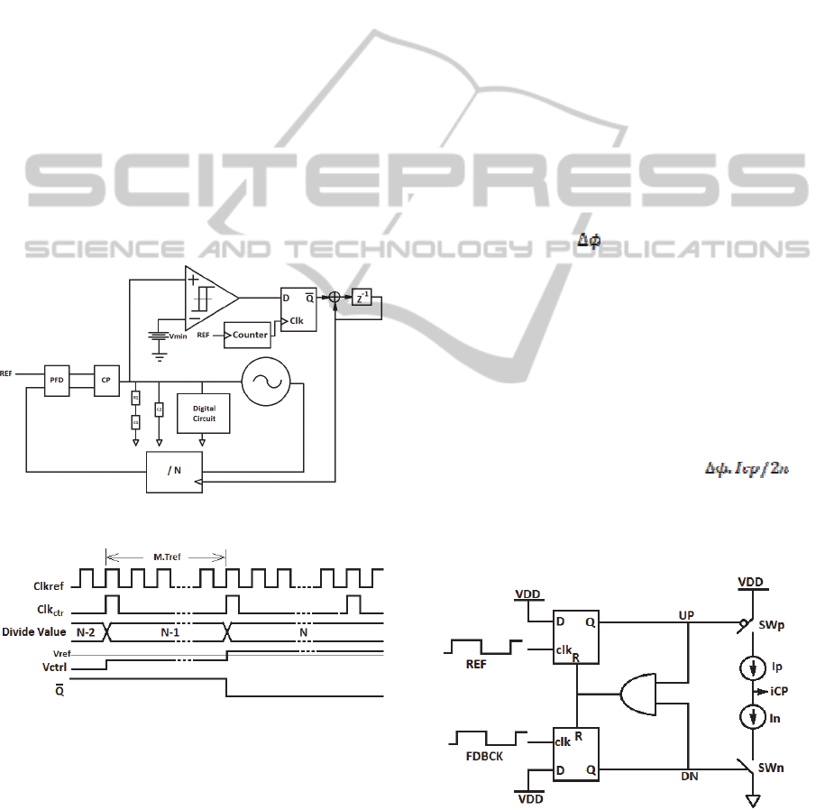
our desired voltage that is minimum acceptable Vctrl
and feeding the result to a digital circuit which sets
the divide value. The comparator should have
hysteresis to avoid feeding wrong data to the next
stage in case of noisy control voltage.
The comparator output is fed to a DFF that is
clocked by a counter. The counter is needed because
after changing the divide value, we should wait
enough to let the loop to settle to its new value and
then do the comparison. This timing can be done by
waiting M cycles of the reference clock. M depends
on the reference clock frequency and PLL
bandwidth. Once the DFF clock input goes high, it
passes the comparator state to its output. If control
voltage is below Vref, the DFF output is one and
causes the divide value to increase by one. Then we
wait for M cycles of the reference clock and sample
the Vctrl again. This procedure continues by the
time that Vctrl goes above Vref and after that the
divide value doesn't change since the DFF output is
always zero. Timing diagram of such architecture
can be seen through Figure 4.
Figure 3: Proposed architecture for control voltage setting.
Figure 4: Timing diagram of the proposed architecture to
set control voltage.
4 DESIGN CONSIDERATIONS OF
PLL BASED TECHNIQUE FOR
POWER SUPPLY ISOLATION
OF THE CRYPTO-PROCESSOR
A low power phase locked loop (PLL) is designed in
order to supply the crypto-processor through its
control voltage line. This PLL consists of a low
power current-starved ring oscillator VCO which
operates at low frequency, a charge pump based
PFD and a second-order loop filter. In the rest of this
section, circuit details are briefly explained.
4.1 PFD
Phase frequency detector (PFD) architecture is
shown in Figure 5. It is composed of two DFFs and
a charge pump that acts as the comparator between
the phase of the reference and output signals.
Assume the output signal is lag respect to the
reference signal by
. Once the reference signal
comes in, the output of the top DFF goes high.
Feedback signal triggers the bottom DFF at its rising
edge which leads to both DFFs get reset through the
AND gate since both UP and DN signals are high.
Therefore, by using this circuit, we could generate a
pulse whose pulse width is proportional to the initial
phase difference between two clocks. When UP goes
high, it turns ON the top current source in the CP
and DN signal, disables that. As a result, by
employing a charge pump, a current pulse with
amplitude of Icp and pulse width of
is
generated and passed to the next block that is loop
filter. The value of the charge pump current is
chosen based on the required PLL bandwidth and its
phase margin.
Figure 5: PFD along with charge pump configuration.
Transistor level implementation of the charge
pump can be seen through Figure 6. MP1 and MN1
are the top and bottom current sources which are
DPAResistanceEnhancementthroughaSelf-healingPLLbasedPowerMask
269
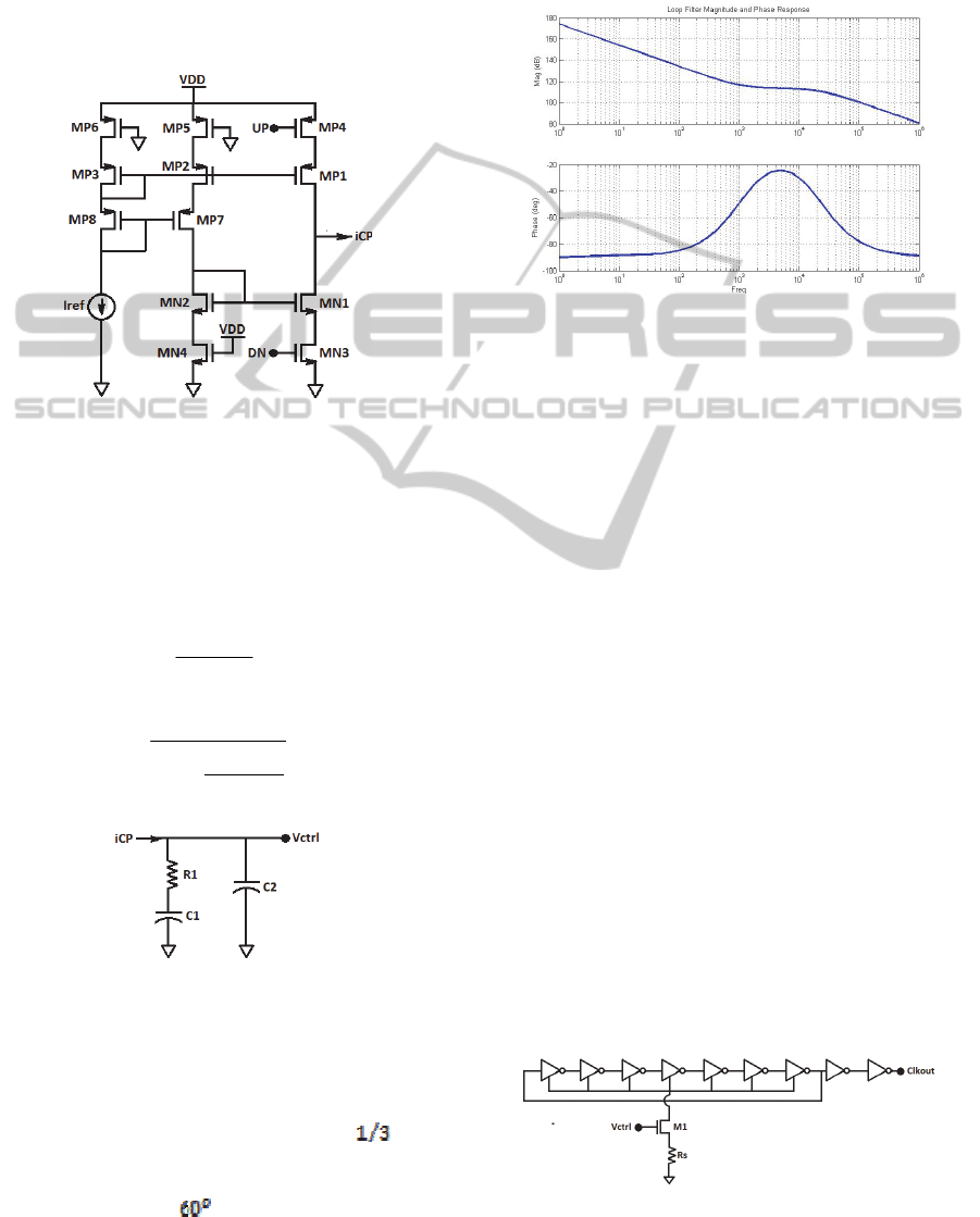
gated by MP4 and MN3 and they are carrying 10nA
current during ON time. That current is mirrored
from Iref through MP3 and MP2 into the CP core.
MP5-6 are added to replicate MP4 for maximum
matching between all the branches. MP7-8 are
making the drain voltages of MP2-3 close enough in
order to have identical currents flowing at the left
two branches.
Figure 6: Transistor level implementation of charge pump.
4.2 Loop Filter
Loop filter structure can be seen through Figure 7. It
has two capacitors and one resistor. Therefore it
gives us a transfer function that has one zero and one
pole at the following frequencies:
2
1
11
CR
f
z
(1)
21
21
1
2
1
CC
CC
R
f
p
(2)
Figure 7: Loop filter employed in the PLL structure.
The loop filter capacitor should be big since it is
direct power source of the digital circuit. This leads
us toward designing a low-bandwidth PLL. In this
design loop bandwidth is supposed to be about
3kHz, the zero is placed at 1kHz which is
of the
UGB of the PLL open loop transfer function. The
pole location is chosen based on the required phase
margin that is about
and it results in the pole
frequency of about 20kHz. The resistor value is low
enough to have minimal reference feed through
while keeping the capacitors sized reasonably high.
The loop filter magnitude and phase is shown in
Figure 8.
Figure 8: Phase and frequency of loop filter.
4.3 VCO
A low power oscillator that operates at low
frequencies is required for this design. Ring
oscillator and LC-Oscillator are the two types of
oscillators which are commonly used in PLL design.
LC-Oscillator is the preferred architecture whenever
the phase noise requirement is tight and this comes
at the cost of higher area due to having inductor and
capacitor tank and usually less frequency coverage
range. Also, it burns more power since it has
negative-gm circuit. On the other hand, ring
oscillator is a better option for applications in which
phase noise number is not that tight but power and
area is a constraint. Our design falls in the second
category since we are not using the VCO output
signal anywhere; hence phase noise performance is
not important. Also operating at very low power
mode is mandated as the main purpose of having the
PLL is just to supply the digital circuit and definitely
it should consume as low power as possible.
Figure 9 illustrates the VCO architecture in this
project. It’s a current-starved ring oscillator with
seven stages in the loop.
The VCO core signal is buffered and sent out to
be used in the feedback path. The V-to-I branch is a
NMOS device which is degenerated by resistor Rs.
Figure 9: Seven-stage ring oscillator.
SECRYPT2015-InternationalConferenceonSecurityandCryptography
270
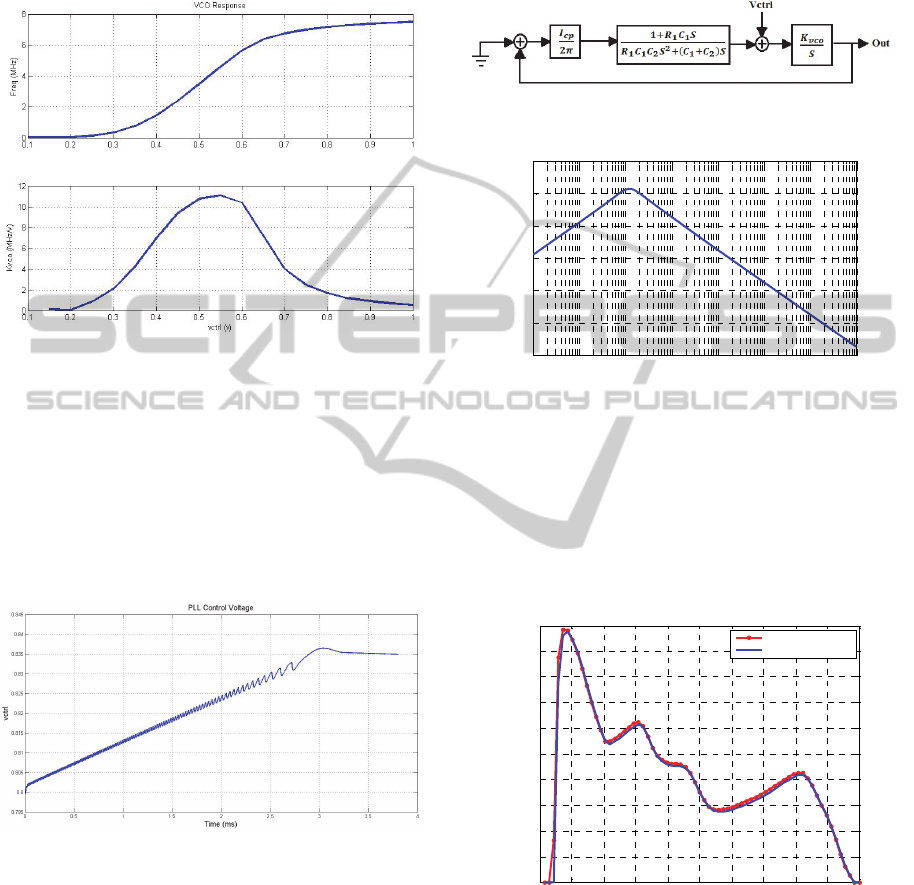
The VCO is designed in a way to get a
reasonable Kvco at a center frequency equal to
8MHz. Figure 10 shows VCO frequency and Kvco
vs control voltage.
Figure 10: VCO frequency and Kvco vs control voltage.
5 SIMULATION RESULTS
As mentioned before when the loop is locked,
control voltage stays constant to a value which
forces the oscillator to generate a signal whose
frequency is equal to the reference frequency. PLL
control voltage can be seen through Figure 11.
Figure 11: PLL control voltage.
The minimum acceptable supply voltage for
crypto-processor is 0.75V and since PLL settled at
0.83V no change is needed in divider value.
In most of the existing masking techniques, the
activity of the crypto-processor block can be leaked
through capacitor coupling to the other part of the
circuit. However, in the proposed PLL based
technique, all the high frequency activities will get
filtered due to band-pass characteristic of output to
control voltage. This guarantees complete masking
of the crypto-processor from the possible capacitor
coupling between input/output of the VCO block.
PLL block diagram when the input is grounded and
PLL output to control voltage transfer function are
shown respectively in Figure 12 and Figure 13.
Figure 12: PLL block diagram.
10
1
10
2
10
3
10
4
10
5
10
6
10
7
10
8
-40
-20
0
20
40
60
80
Freq (Hz)
Gain (dB)
PLL Output to Vctrl Transfer Function
Figure 13: PLL output to Vctrl transfer function.
Our final goal in designing such architecture is
de-correlating power consumption from supply
voltage so the last step is observing the current
which is driven from the supply voltage when clock
is applied to the crypto-processor. Figure 14 shows
one current pulse which is taken from supply voltage
before and after adding the crypto-processor.
0 0.2 0.4 0.6 0.8 1 1.2 1.4 1.6 1.8 2
0
0.2
0.4
0.6
0.8
1
1.2
1.4
1.6
1.8
2
time[ps]
current[mA]
PLL+Crypto Processor
PLL Only
Figure 14: PLL supply current before and after adding the
crypto-processor.
As can be seen through Figure 14, the current
driven from supply before and after adding the
crypto-processor stays almost constant because the
encryption circuit is completely isolated from the
power supply that might be visible to the attacker.
Moreover since the PLL designed for this
DPAResistanceEnhancementthroughaSelf-healingPLLbasedPowerMask
271

architecture is low bandwidth, high frequency
components of crypto-processor current will not
appear at the output of the VCO.
It’s also important to mention that the total charge
taken from supply voltage by the PLL circuit with
the crypto-processor is equal to the charge that the
PLL and crypto-processor take from supply voltage
separately however their current profile is different.
The crypto-processor applied to the PLL in this
design is a 4 bit SBOX implemented with dual rail
current mode differential logic. This PLL based
architecture burns 10.69 μW power at 1 volt supply
voltage.
6 CONCLUSION
This paper presents a new design for smart cards
security realizations. The proposed structure is based
on a low bandwidth phase locked loop to make
power consumption of a cryptographic system
independent from algorithm operation. Simulation
results confirm that by employing this technique
while securing the secret key, total cost and area do
not increase significantly.
REFERENCES
Shamir, A., 2000, ‘Protecting smart cards from passive
power analysis with detached power supplies’, proc.
2
nd
Int. Workshop on Cryptographic Hardware and
Embedded Systems, pp. 7177.
Tiri, K., Akmal, M., Verbauwhede, I., 2002, ‘A Dynamic
and Differential CMOS Logic with Signal
Independent power consumption to withstand
differential power analysis on smart cards’, Proc. 28
th
European solid state Circuits Conf, pp. 403-406.
Li, H., Ma, G., Li, G., Wang, G., Zhou, T., 2007, ‘A New
Protect Cryptographic Circuit Approach Using
Dynamic Current Model Logic Circuit’, International
conference on mechatronics and automation ICMA,
pp. 2221-2225.
Zadeh, A. K., Gebotys, C., Ardalan, S., 2011,
‘Counteracting power analysis attack using Static
Single-ended Logic’, IEEE International Symposium
on Circuits and Systems ISCAS, pp.721-724.
Toprak, Z., Leblebici, Y., 2005, ‘Low-power current mode
logic for improved DPA-resistance in embedded
systems’, IEEE International Symposium on Circuits
and Systems ISCAS, pp. 1059-1062.
Cocher, P., Jaff, J., Jun, B., 1999, ‘Introduction to
differential power analysis’, Proc. 19
th
Ann. Intl
Cryptography Conference, pp. 388-397.
Messerges, T., Dabbish, E., Sloan, R., 2002, ‘Examining
Smart Card Security under the treat of power analysis
attacks’, IEEE Trans. Computers, vol.51, No.5, pp.
541-552.
Corsonello, P., Perri, S., Margala, M., 2006, ‘An
integrated countermeasure against differential power
analysis for secure smart-cards’, IEEE International
Symposium on Circuits and Systems ISCAS, pp. 21-24.
Tokunaga, C., Blaauw, D., 2010, ‘Securing Encryption
Systems With a Switched Capacitor Current
Equalizer’, IEEE Journal of Solid-State Circuits,
vol.45, no.1, pp.23-31.
SECRYPT2015-InternationalConferenceonSecurityandCryptography
272
