
Tunable Mirror and Multi-channel Filter Based on One-dimensional
Exponentially Graded Photonic Crystals
Bipin Kumar Singh and Praveen Chandra Pandey
Department of Physics, Indian Institute of Technology (Banaras Hindu University), Varanasi, 221005, India
Keywords: Graded Photonic Crystals, Photonic Band Gap, Omni-directional Band Gap, Exponential Graded Materials.
Abstract: A study on the tunability of photonic and Omni-directional band gaps has been demonstrated theoretically
in one-dimensional (1-D) photonic crystals having one of the layers as exponential graded index materials
and other layers of constant refractive index materials. Using numerical simulations, we have investigated
the effect of relative parameters of exponential graded layers on the photonic and Omni-directional band
gaps in 1-D graded photonic crystals (GPCs). We observe that the number of photonic band gaps increases
with increase of the layer thicknesses and their bandwidths can be controlled by the contrast between initial
and final refractive index of the graded layers. Moreover, we have studied the Omni-directional band gaps
in quarter-wave and latent type layer stacking arrangements. Further, we obtained the range of refractive
indices and thicknesses of constituted layers at which omnidirectional band gaps occurs. Accordingly, we
find that the photonic as well as Omni-directional band gaps of desired bandwidths can be obtained by
selecting appropriate parameters in GPCs. Our work will be useful in design of mirrors, channel filters,
Optical sensors, Omni-directional reflectors etc. and provide more design freedom for alternative photonic
devices.
1 INTRODUCTION
The propagation of light through a periodic medium
has been widely researched since the appearance of
photonic crystal (PC) materials (Yablonovitch,
1987). PCs are structures composed of two or more
materials with different refractive index and
arranged in a periodic configuration that forbids the
propagation of electromagnetic waves in certain
frequency ranges. This leads to a range of frequency
where no electromagnetic mode exists within the
PCs, is called photonic band gap, which is analogous
to the electronic band gap in conventional
semiconductors (Joannopoulos, 1997). This property
can be used to confine, manipulate and control
photons in PCs, and expected to be a key technology
for all integrated optical devices (Lipson, 2009).
Over the past several years, 1-D PCs have been
intensively investigated with different materials such
as dielectric, anisotropic, negative refractive index,
magneto materials etc. in periodic or non-periodic
arrangements (Tolmachev, 2008, Negro, 2005,
Alagappan, 2006, Zharov, 2008, Vasconcelos, 2007,
Yu, 2007 and Macia, 2012). These have many
potential applications in optical communication and
optoelectronics such as reflecting mirrors,
waveguides, optical switches, filters, detectors,
limiters, light emitting diode etc. Moreover, one of
the major interesting application of the PCs is the
property of Omni-directional reflection by which
light with some frequency region from all of the
incident angle is totally reflected for both of the TE
(Transverse electric) and TM (Transverse magnetic)
polarization. The absolute Omni-directional
photonic band gap has been demonstrated
theoretically and experimentally in 1-D PC
structures (Fink, 1998, Yablonovitch, 1998, Seeser,
1999, Xiang, 2010). The Omni-directional band gap
has potential applications in reflectors, filters and
optical fibers etc.
Recently several other researchers have been
proposed the 1-D multilayer structures, in which
refractive index or width of layers varies in the form
of gradual fashion along the direction perpendicular
to the surface of layer (Rauh, 2010, Sang, 2006,
Pandey, 2008, Rauh, 2012, Singh, 2013). Such type
structures are called graded photonic crystals
(GPCs). Gradual variation of relative parameters in
GPCs makes them very different in the behaviour
from the conventional PCs and enhances the ability
to mold and control of the light wave propagation.
22
Singh B. and Pandey P..
Tunable Mirror and Multi-channel Filter Based on One-dimensional Exponentially Graded Photonic Crystals.
DOI: 10.5220/0005333600220033
In Proceedings of the 3rd International Conference on Photonics, Optics and Laser Technology (PHOTOPTICS-2015), pages 22-33
ISBN: 978-989-758-093-2
Copyright
c
2015 SCITEPRESS (Science and Technology Publications, Lda.)
Graded index materials in one dimensional quasi-
periodic photonic crystal have great influence on the
optical reflectance and localization modes (Singh,
2014, Singh, 2014).
Motivated by the ability to mold, confine and
control of the electromagnetic waves by different
types of GPCs. Herein, we study the photonic and
Omni-directional band gap characteristics in 1-D
GPCs constituted with exponentially graded
dielectric layer. Refractive index in exponentially
graded layers varies in the form of exponential
fashion as a function of the depth of graded layer.
This paper is arranged as follows: In Sec. II, the
theory and calculation of the reflectance and band
structure of 1-D GPC structures is provided. In Sec.
III, we investigate the influence of exponentially
graded layers on the photonic and Omni-directional
band gap properties of 1-D GPC structures. In this
Section, our study has been carried out in three
steps. First, we present the reflection spectra and
band structure of 1-D GPC structures for different
layer thicknesses and various refractive index of the
constituted normal layer. Second, we investigate the
properties of Omni-directional band gap for quarter-
wave and latent type layer stacking arrangements.
Next, we study the effect of the contrast of initial
and final refractive index of the exponential graded
layer on the photonic band gap of 1-D GPC
structures. Finally, in section IV we have briefly
summarized the results.
2 THEORETICAL DESCRIPTION
Here, we present the 1-D GPC multilayer structures
as shown in Fig. 1. The GPCs considered in our
investigation are composed of two types of dielectric
layers. One is the graded layer (A or Aʹ) with
exponential varying refractive index as a function of
depth of layer and other is homogeneous layer (B)
with space independent refractive index. Refractive
index profile in the considered exponential graded
layers varies in two ways with depth of layer. First,
index of refraction increases exponentially from
initial to end boundary of the graded layer and is
represented as;
(
)
=
exp
ln
(1)
Second, when refractive index decreases
exponentially from initial to final boundary of the
graded layer, it can be expressed as;
(
)
=
exp
ln
(2)
Where
and
is the lower and higher index of
refraction, respectively and
is the layer thickness.
In our proposed structures, first case is considered in
layer ‘A’ and second case in layer ‘Aʹ’. The two
representative structures of 1-D GPCs are a
multilayer structure composed with layer A and Aʹ,
and their schematic diagram are illustrated in Fig.
1(a) and 1(b), respectively. Refractive index
variation in relative proposed structures is also
shown in Fig. 1.
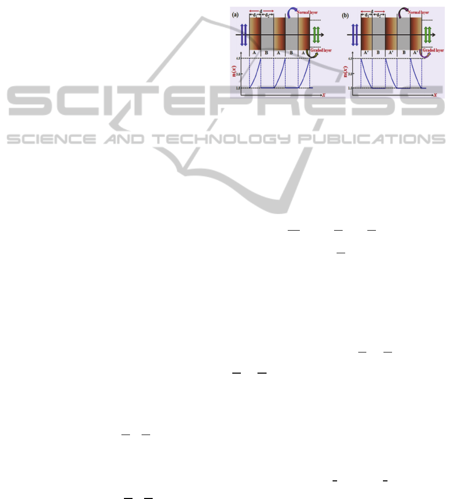
Figure 1: The schematic representation of 1-D graded
photonic crystals with exponentially (a) increasing and (b)
decreasing refractive index along the thickness of
exponential graded layer.
The wave equation for light wave propagation in
graded layer, which has exponentially varying
refractive index along the plane perpendicular to the
surface of layer (suppose x-direction) can be written
as
+
+
= 0 (3)
Where, =
(
)
is the wave
propagation vector for exponential graded layers at
normal angle of incidence. Refractive index
(
)
taken according the exponential graded layers with
increasing and decreasing refractive index defined as
above equations (1) and (2), respectively and λ is the
wavelength of light. Grading profile parameter for
exponentially increasing and decreasing refractive
index layers to be =
ln
andʹ =
ln
, respectively. Therefore, we can represent
the equation (1) and (2) for the variation of
refractive index in the exponential graded layers (A
and Aʹ) as
(
)
=
or
ʹ
for increasing or
decreasing order, respectively. (Yeh, 1988)
The solution of equation (3) can be expressed for
increasing refractive index in the exponential graded
layers as
()=
+
(4)
Where
and
are arbitrary
TunableMirrorandMulti-channelFilterBasedonOne-dimensionalExponentiallyGradedPhotonicCrystals
23

constants for graded layers,
and
are first and
second kind of the zero-order Bessel function,
respectively. Subscript G represents a graded layer.
Similarly,the solution for exponential graded
layers with decreasing refractive index to be similar
as equation (4) only propagation wave vector and
grading profile parameter changes according to this
layer.
The electric field distribution for a homogeneous
layer along x-axis can be written as
=
exp
(
−
)
+
exp
(
)
(5)
Where, A
H
and B
H
are the arbitrary constants,
is the wave vector and at normal angle of incidence
=
. Subscript H represents a homogeneous
layer.
To investigate the propagation properties of the
electromagnetic wave in the periodic structures
(AB)
N
and (AʹB)
N
, where N is the number of
periods. We embrace the transfer matrix method to
calculate the reflectance and band gap spectra. After
applying the transfer matrix approach on the
considered structures, if refractive index increases
exponentially with depth of graded layers, the
electromagnetic wave propagate through the whole
structures can be expressed by multiplying the
characteristic matrices of the constituent layers as
=
.
(
.
)
.
0
(6)
Similarly, for the second case if refractive index
decreases exponentially with depth of graded layers
=
.
(
ʹ
.
)
.
0
(7)
Where N is the number of the period, A
0
, B
0
and
A
N+1
are the arbitrary constant for incident (0
th
)
media and outgoing (N+1)
th
media, respectively.
Matrix
and ʹ
are the characteristics matrix of
exponentially increases and decreases refractive
index with depth of graded layers, respectively.
Matrix
and M
0
is the characteristics matrix of
homogeneous layers and air media, respectively.
The reflection and transmittance coefficient of
the structures, respectively can be written as
=
and =
(8)
Naturally, due to our consideration of lossless
dielectric material, the transmittance here is just the
reflectance’s complement.
A periodic layer structure is equivalent to a one-
dimensional lattice that is invariant under the lattice
translation. Here, refractive indices of layers are
unchanged by the translation of the wave vector by a
lattice constant d, where d is the total thickness of
the periodic system. Using the Floquet’s theorem,
the solution of the wave equation of a period of the
electric field for a periodic layer system can be
written as
(
,
)
=
(
)
.
..–..
, where
is periodic with period d, i.e.
(
+
)
=
(
)
and constant K is known as the Bloch wave
number. Hence the dispersion relation for a periodic
layer medium can be written as
(
,
)
=
.cos
(
+
)
(9)
Where d is the total thickness of a period of the
periodic system, M
and M
is the elements of the
optical transfer matrix
(, = 1,2). Here, Optical
transfer matrix (
) of a period equal to
.
and ʹ
.
for considered structures with
exponentially increasing and decreasing of the
refractive index between the boundaries of the
exponential graded layer, respectively.
The dispersion relation exhibits multiple spectral
bands classified into two regimes: First, where
|(
+
)
/2
|
≤1 corresponds to real K and
thus to propagating Bloch waves. Second, spectral
bands within which K is complex correspond to
evanescent waves that are rapidly attenuated.
Defined by the condition
|(
+
)
/2
|
>1,
these bands correspond to the stop bands also called
photonic band gaps/forbidden gaps since
propagating modes do not exist for the systems.
[Yeh, 1988].
3 NUMERICAL RESULTS AND
DISCUSSION
In this section, we present some numerical results to
characterise the optical reflection, band structures,
phase shift and Omni-directional band due to the
relevant structural parameters of considered 1-D
GPC structures. We consider the medium B as
homogeneous layer with variable refractive index
equal to 1.0, 1.5 and 2.0, while for medium A or A'
(Graded layer), we have exponentially varying
refractive index with depth of layer in increasing
(for layer A) and decreasing (for layer A') fashion
between lower refractive index,
=1.5and higher
refractive index,
= 4.5,as expressed by equation
(1) and (2), respectively. In this study, we assume
that light incident through the air medium and
materials are lossless dielectric. Our results
observation for the considered 1-D GPC structures
constituting exponentially graded index layers has
been carried out in three parts.
PHOTOPTICS2015-InternationalConferenceonPhotonics,OpticsandLaserTechnology
24
3.1 Effect of Layer Thickness on
Photonic Band Gaps in 1-D GPC
Structures
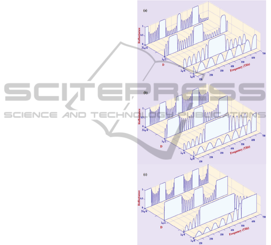
We first present the reflection spectra of 1-D GPC
structures at different layer thickness for some
selected refractive index of homogeneous layer B
under normal incident angle. Thicknesses of the
homogeneous and graded layers are chosen as to
give,
=
=, where
and
are the
thickness of the graded and homogeneous layer,
respectively and
is the mean value of the initial
and final refractive index of the graded layer. For
various layer thicknesses, we choose D as λ
0
/8, λ
0
/4,
λ
0
/2 and 3λ
0
/4, where λ
0
is the optical wavelength
and equal to wavelength for the mean value (450
THz) of the considered frequency region (150-750
THz). If layer thicknesses with relative refractive
index in structures follow the condition that the layer
has an optical thickness one–quarter of the optical
wavelength of light, is called quarter-wave layer
stacking structures. Similarly, if layer thicknesses
with relative refractive index in structures follow the
condition that the layer has an optical thickness half
of the optical wavelength of light, is known as latent
type layer stacking structures. Both type of stacking
structures are very useful and suitable for designing
various photonic devices. As is evident from the
results shown in Fig. 2, there exist a number of
photonic bands, where electromagnetic waves
cannot be transmitted. The number of photonic
bands increases with increasing the thickness of the
layers for each chooses refractive index of the
homogeneous layer B. Because, with increasing the
thickness of layer, the rate of change of refractive
index in graded layers increases, and the average
refractive index over the volume of each graded
layer becomes large. Namely, the rate of change of
refractive index contrast of the two types of
dielectric layer is enhanced and hence influence the
Bragg stack effectively. We also observe that
formation reflection spectra are same for the
structures with both exponential graded layer A and
Aʹ. Fig. 2(a), 2(b) and 2(c), respectively show the
reflection spectra of the considered structures for
constituted homogeneous layer refractive index,
= 2.0, 1.5 and 1.0. For all the chosen refractive index
of the homogeneous layer B, formation of photonic
bands is similar under normal angle of incidence, but
width of bands is different. Bandwidths are larger
for
=1.0as compare to other
values equal to
1.5 and 2.0. Bandwidths are decreases with
increasing
values because the photonic band gap
properties are basically affected by the contrast of
refractive index of constituted media. Contrast of
refractive index of homogeneous layer and graded
layer is higher for
=1.0as compare to other,
therefore the Bragg stack is more effectively and
widths of photonic band are large.
Figure 2: Reflectance spectra of the considered 1-D graded
photonic crystal structures for the constituted
homogeneous layer refractive index (a)
= 1.0, (b)
=
1.5 and (c)
= 2.0, with various layer thickness constant
D.
Now, we examine the confinement effects
arising from competition between the structures
induced by changing the thickness of layers and
magnitude of the total photonic bandwidths in the
photonic band gap spectra. To do that, we calculate
the regions for forbidden frequencies (stop bands),
where
|(
+
)
/2
|
>1, as a function of the
TunableMirrorandMulti-channelFilterBasedonOne-dimensionalExponentiallyGradedPhotonicCrystals
25
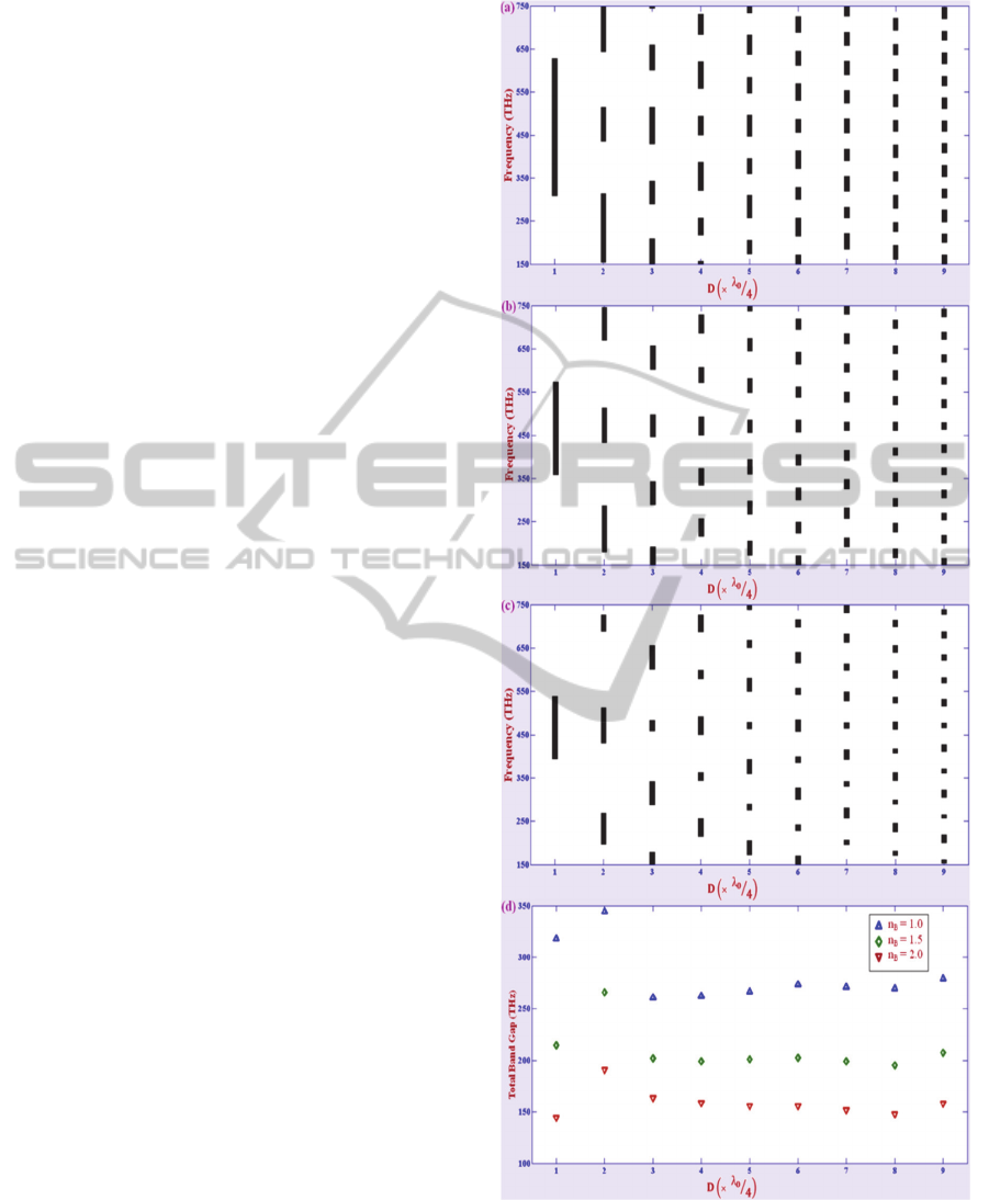
thickness of the layers is depicted in Fig. 3(a), 3(b)
and 3(c) for the structures with various refractive
index of homogeneous layer
equal to 1.0, 1.5 and
2.0, respectively. These figures show the distribution
of the forbidden (black region) and allowed (white
region) frequencies, as a function of the thickness of
layers for the structures with
equal to 1.0, 1.5 and
2.0 up to the value of D = 9λ
0
/4. Note that, as
expected for large layer thicknesses, we get number
of forbidden bands and their bandwidths become
narrower and narrower as an indication of more
photonic band gaps with small bandwidths. We
observe number of forbidden bands are approximate
same for the structures with acceptable
-values
but their bandwidths are different. Total bandwidths
in the structures with
=1.0 are maximum as
compare to other considered
-values, which is
clearly demonstrated in Fig. 3(d). In this figure, we
show the total band gap verses the layer thickness
constant (D) for the structures with various
refractive index (
) of homogeneous layer. It
reveals that the total band gaps randomly change
with increasing the layer thicknesses, but it is
extremun for considered structures with latent type
layer stacking arrangements. Therefore, these type
structures can be used as mirrors and multi-channel
filters by adjusting the layer thicknesses.
For better understanding the effect of graded
layer arrangements in the considered 1-D GPCs, we
have also calculated the spatial distribution of the
square magnitude of the electric field at three
selected frequencies impinging under ≈0%, ≈50%
and ≈100% reflection conditions for the structures
(AB)
10
and (A'B)
10
, as demonstrated in figure 4. The
electric field is denoted by E(x). For the sake of
clarity, we have chosen the thickness of layers with
relative refractive index equal to 5λ
0
/4, so the effect
of electric field can be better appreciated. From the
reflection spectra of the structures with
=1.0, it
can be clearly observed that at the spectral band
edge positions 635THz, where close to 0% reflection
is found, reflection is stronger ≈100% within the
band gap region than that observed for frequencies
580THz inside the band gap, and at one of the peak
at 628.4THz where ≈50% reflection is observed.
Therefore, electric field intensity within the
considered structures for frequencies 635THz,
628.4THz and 580THz is demonstrated in figure
4(a), 4(b) and 4(c), respectively. Panels (i) and (ii) of
the figure 4 show the distribution of electric field
intensity in the periodic structures (AB)
10
and
(A'B)
10
, respectively. It is shown that the electric
field distributions in exponential graded layers for
different grading profiles are quite different,
Figure 3: The distribution of the bandwidths as a function
of the layer thickness constant D for the structures with
homogenous layer refractive index (a)
= 1.0, (b)
=
1.5 and (c)
= 2.0, and plot (d) show the total band gap
of the forbidden band regions against the layer thickness
constant D.
PHOTOPTICS2015-InternationalConferenceonPhotonics,OpticsandLaserTechnology
26
although the volume-average refractive index is
same. For exponentially increasing refractive index
profile, the electric field intensities in exponential
graded layers decrease as propagating depth
increases as seen in panels (i), while intensities
increase as increases propagating depth for
exponential decreasing refractive index as depicted
in panels (ii). The reason is the effect of the
inhomogeneity in the exponential graded layers. On
the other hand, the variation of electric field
intensities in graded layers changes due to the space
dispersive increasing or decreasing refractive index
with graded layers depth. In addition, the electric
field intensities in non-graded layers keep
unchanged for both types of periodic structures
(AB)
10
and (A'B)
10
.
Figure 4: Panels (i) and (ii), respectively show the spatial
distributions of the electric field intensity in the systems
type1 (AB)
10
and type2 (A'B)
10
at three selected
frequencies (a) 580 THz, (b) 628.4 THz and (c) 635 THz,
impinging under ≈0%, ≈50% and ≈100%, respectively.
Due to the importance of the widespread
photonic band gaps for the 1-D GPC structures, we
would like to extend the study on the dispersion
curves and reflection phase shift associated with the
wider photonic band gaps in structures with
=
1.0. For different layer thicknesses, dispersion
curves are calculated from equation (9) for the
unbounded periodic structures and shown in panels
(i) of Fig. 5 as functions of the reduced Bloch wave
vector kd/π, and related reflection phase shifts are
likewise illustrated in panels (ii) of the Fig. 5. As
expected, the band gaps observed at zero
transmission intensity range. The corresponding
dispersion curves for the finite crystal are depicted
in panels (i) of Fig. 5(a), 5(b) and 5(c), respectively
for layer thickness with relative refractive index
proportional to λ
0
/4, λ
0
/2 and 3λ
0
/4. Also as seen
here, number of bands increases with increase in
layer thicknesses, single band formed for layer
Figure 5: Panels (i) and (ii), respectively show the
dispersion relationship and phase shifts in a photonic
crystal with unit cell consisting of one layer of
exponentially graded index material (
=1.5 to
= 4.5)
and other layer of air, for optical layer thicknesses with
relative refractive index equal to (a) λ
0
/4, (b) λ
0
/2 and (c)
3λ
0
/4.
TunableMirrorandMulti-channelFilterBasedonOne-dimensionalExponentiallyGradedPhotonicCrystals
27
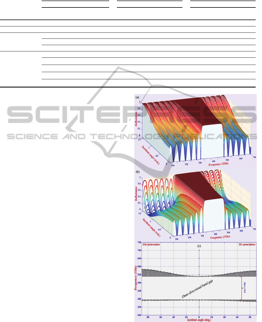
Table 1: Reflection bands region and bandwidths in the GPC structures at normal incidence for different layer thickness.
Layer
thickness
constant (D)
Structures with n
B
= 2.0 Structures with n
B
= 1.5 Structures with n
B
= 1.0
Reflection
Band Region
Reflection
Band Width
Reflection
Band Region
Reflection
Band Width
Reflection
Band Region
Reflection
Band Width
λ
0
/8 ………. …… 750.0 – 719.0 31 750.0 – 617.8 132.2
λ
0
/4 538.0 – 393.8 144.2 574.0 – 359.6 214.4 627.0 – 309.0 318
λ
0
/2
269.0 – 197.0 72 287.0 – 179.8 107.2 313.4 – 154.6 158.8
512.2 – 431.2 81 514.0 – 432.6 81.4 514.8 – 435.4 79.4
725.8 – 688.4 37.4 746.2 – 669.2 77 750.0 – 643.6 106.4
3λ
0
/4
179.2 – 150.0 29.2 191.2 – 150.0 41.2 209.0 – 150.0 59
341.8 – 287.6 54.2 342.4 – 289.2 53.2 343.2 – 290.2 53
483.8 – 459.0 24.8 497.4 – 446.2 51.2 515.6 – 429.2 86.4
655.8 – 601.0 54.8 656.6 – 601.2 55.4 658.6 – 601.0 57.6
……………… …………….. 750.0 – 745.0 5
thickness with relative refractive index equal to λ
0
/4,
three bands for λ
0
/2 and four broader bands for
3λ
0
/4, but the bandwidths become narrow with
increasing the number of bands. The forbidden
bands region and bandwidths of the structures for
different layer thicknesses and various refractive
index of the homogeneous layer B are listed in Table
1. Moreover, we watch in panels (ii) of Fig. 5 and
observe that reflection phase shifts varies from close
to –π at one band edge to approximate π at another
band edge of the stop bands for the precise
arrangement of unit cells in structures. Here, we
have investigated reflection phase shifts for one of
the specified possible arrangements of layers in a
period of the considered graded photonic crystal
structures.
According to our results, we observe that
reflection, transmission and photonic band gap
spectra are independent on the arrangement of
graded layers (A or A') in unit cells of the structures,
whereas field distributions and reflection phase
shifts change with arrangement of graded layers in
unit cells of the structures.
3.2 Study of the Omni-Directional
Band Gap in 1-D GPC Structures
In this section, we discuss the Omni-directional band
gap characteristics in the proposed 1-D GPC
structures, which have quarter-wave and latent type
layer stacking arrangements. An Omni-directional
band gap can be obtained within a specific
frequency range in photonic crystal as a forbidden
band gap that reflects electromagnetic wave at any
incident angle for both TE and TM-polarization.
The dependence of photonic band gaps on the
incident angle in a quarter-wave stacking multilayer
structures for TE and TM polarization are shown in
Fig. 6(a & b), 7(a & b) and 8(a & b) for various
Figure 6: Reflection spectra for (a) TE-polarization, (b)
TM-polarization and (c) projected reflection band
structure as the changing of the incident angle of the
quarter-wave stacking structure with
= 2.0.
PHOTOPTICS2015-InternationalConferenceonPhotonics,OpticsandLaserTechnology
28
refractive index;
= 2.0, 1.5 and 1.0, respectively.
These figures are clearly demonstrated that the
expansion of photonic band gap in structures with
= 2.0 and 1.5 are enhance for both TE and TM-
wave, while for
= 1.0, photonic band spreading
in frequency range for TE-wave and shrinking in
frequency range for TM-wave, when the incident
angle increases.
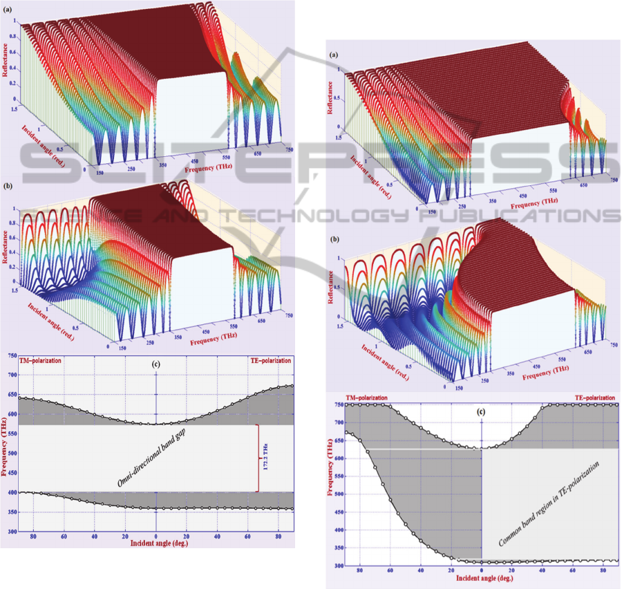
Figure 7: Reflection spectra for (a) TE-polarization, (b)
TM-polarization and (c) projected reflection band
structure as the changing of the incident angle of the
quarter-wave stacking structure with
= 1.5.
In order to discuss the Omni-directional band gap
properties of the structures, we have plotted the
projection band structures as changing of the
incident angle and exhibited in Fig. 6(c), 7(c) and
8(c), respectively for the structures with
= 2.0,
1.5 and 1.0. From these figures, we can clearly
inspect the variation of higher and lower band edges
as changing of the incident angle. There is an Omni-
directional band gap, which exists between higher
and lower band edges as prevalent band region for
both TE and TM-polarization. The photonic band
spectra of the photonic crystals can be usually
achieved from the projection of unit reflectance from
Fig. 6(a & b), 7(a & b) and 8(a & b), and Omni-
directional band gap clearly demonstrated in Fig.
6(c), 7(c) and 8(c).
Figure 8: Reflection spectra for (a) TE-polarization, (b)
TM-polarization and (c) projected reflection band
structure as the changing of the incident angle of the
quarter-wave stacking structure with
= 1.0.
In Fig. 6(c), 7(c) and 8(c), the grey areas
represent the forbidden band for relative polarization
and the ubiquitous white area between the band
TunableMirrorandMulti-channelFilterBasedonOne-dimensionalExponentiallyGradedPhotonicCrystals
29

Table 2: Omni-directional bands region and bandwidths in the GPC structures for various
- values.
Structures
with
Layer
thickness
constant (D)
Complete Band Region in
Omni-directional
Band Region
Omni-directional
Band Width
TE-Polarization TM-Polarization
n
B
= 2.0
λ
0
/4 538.0 – 393.8 538.0 – 393.8 538.0 – 393.8 144.2
λ
0
/2
269.0 – 197.0 269.0 – 197.0 269.0 – 197.0 72
512.2 – 443.0 512.2 – 464.6 512.2 – 464.6 47.6
725.8 – 694.0 725.8 – 696.6 725.8 – 696.6 29.2
n
B
= 1.5
λ
0
/4 574.0 – 360.2 574.0 – 401.8 574.0 – 401.8 172.2
λ
0
/2
287.0 –180.2 287.0 –201.0 287.0 –201.0 86
514.0 – 483.6 514.0 – 502.6 514.0 – 502.6 11.4
746.2 – 715.6 746.2 – 735.4 746.2 – 735.4 10.8
n
B
= 1.0
λ
0
/4 627.0 – 316.8 ………. ………. ……….
λ
0
/2
313.4 – 158.4 ………. ………. ……….
…………….. ………………… ……………... …………………...
edges in both polarizations illustrate the Omni-
directional band gap. It is certified from figures, an
Omni-directional band exist for structure with
=
2.0 and 1.5, while it is not be observed in structure
with
= 1.0. But one obvious feature of this
structure is that there exist broadest complete band
gap for TE-wave. Therefore, structure with
= 1.0
is more suitable for designing TE-polarized photonic
devices and structures with
= 2.0 and 1.5 can be
used for design Omni-directional photonic devices.
Furthermore, we have emphasized the projection
band structure as the changing of the incident angle
for latent type layer stacking multilayer structures
with
= 2.0, 1.5 and 1.0. It is clear from our
charts, as like a quarter-wave stacking structures,
Omni-directional band gap is not exist for structure
with
= 1.0, but it is obtained for structure with
= 2.0 and 1.5. This implies that occurrence of Omni-
directional bands is affected by the contrast of
refractive index between homogeneous and graded
layer, and it is absence for the structures with
=
1.0. The number of Omni-directional bands existed
for these structures with
= 2.0 and 1.5 therefore,
these types of structure can be used in the
widespread Omni-directional photonic devices
which operate in range 150-750 THz. The Omni-
directional bands range and bandwidths for the
quarter-wave and latent type layer stacking
structures with different
-values are tabulated in
Table 2.
Accordingly, we find that refractive indices of
constituted homogeneous layers >1 produce the
Omnidirectional band gaps but increasing the
indices band gaps become narrowest. Thus the
existence of omnidirectional band gaps in graded-
homogenous periodicity approach requires the index
contrast (
−
) for
>1. But, under this
condition, the broader the desired Omnidirectional
band range, the greater the demands on index
contrast (
−
), where
is the mean value of
the initial and final refractive index of the graded
layer and
is the refractive index of the graded
layer. In addition, the omnidirectional band gap can
be adjusted by the modifying the layers thicknesses.
3.3 Effect of the Ratio of
and
on
the Photonic Band Gap
Now, we investigate the dependence of the photonic
band gap on the ratio of initial and final refractive
index i.e.
-value of the exponential graded
layers in 1-D GPC structures under normal angle of
incidence. Here, we considered initial refractive
index (
) is fixed and equal to 1.5, while, final
refractive index (
) varies according to contrast
value between these. In the Fig. 9(a), we have
depicted the refractive spectra for the various
-
values in a quarter wave stacking multilayer
structures with a relatively homogeneous layer
refractive index
=1.0. As expected, the photonic
bandwidth decreases with decreasing the ratio i.e.
-values.The explanation for this phenomenon is
that decreasing the ratio of initial and final index of
refraction of the exponential graded layer, the rate of
modification of the grading profile parameter (γ or
γ') decreases, and corresponding average refractive
index over the volume of each graded layer
conjointly decreases, hence influence the Bragg
stack become less effectively. However, the
photonic band gap decreases with decreasing the
grading profile parameter yet obtained band gap
PHOTOPTICS2015-InternationalConferenceonPhotonics,OpticsandLaserTechnology
30
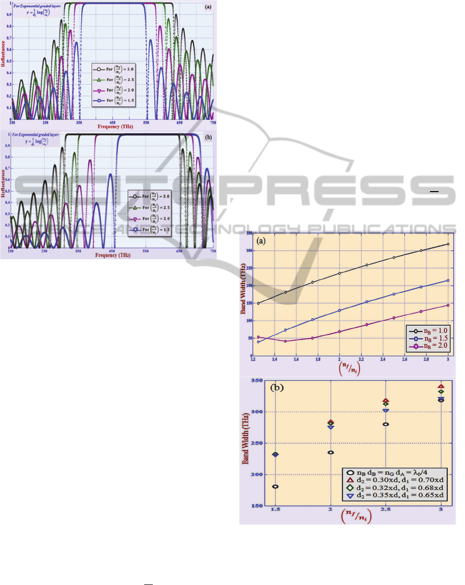
exists around the central frequency and it is
obviously exhibited in Fig. 9(a).
Figure 9: Reflectance spectra for different values of
grading profile parameter γ or γ' of exponential graded
index layer for the structures with (a) quarter wave
stacking and (b) precise layer thickness d
1
= 64 nm and d
2
= 136 nm.
To have a more complete description and a better
understanding of the effect of the ratio of initial and
final refractive index of the exponential graded layer
on the properties of photonic band gap, it is
important to know how these effects change the
properties of the reflection coefficients and photonic
band gap for the structures with specific layer
widths. Here, we also observe that the photonic band
gap diminishes with decreasing the grading profile
parameter but here acquired band gap is shifted
towards the higher frequency region, and it is clearly
demonstrated in Fig. 9(b). The explanation for this
difference between the above-considered structural
arrangements is that, in case of quarter-wave
stacking arrangements, the graded layers thickness
and grading profile parameter change with the ratio
of initial and final refractive index, while in case of
the structures with set layer widths, the width
parameters are independent of the ratio of initial and
final refractive index.
Moreover, we have plotted the forbidden
bandwidth by changing the ratio
for a quarter-
wave stacking multilayer structure with various
relative homogeneous layer refractive indices under
normal angle of incidence, which have been
illustrated in the Fig. 10(a). In this figure, we see
that for a quarter-wave stacking type structures,
photonic bandwidth decreases almost linearly.
Diminishing of photonic bandwidths is observed for
all values of the refractive index ratio greater or
equal to the refractive index of the homogeneous
layer. But, when the refractive indices ratio of the
graded layer becomes lesser than the value of the
refractive index of the homogeneous layer than
forbidden band width increases gradually and it is
clear from third graph for
= 2.0 in Fig. 10(a).
This reason is the effect of the increase in contrast of
the refractive indices of the homogeneous and
graded layer. To have a better understanding of the
effect of the refractive index ratio on the photonic
bandwidths, we have also demonstrated the photonic
bandwidths variation by changing the ratio
for
the structures with different precise layer widths,
and it is clearly exhibited in Fig. 10(b). From
Figure 10: Panel (a) shows the distribution of the
bandwidths as a function of the ratio
⁄
for the
quarter wave stacking structures with different considered
-values and (b) exhibits the distribution of the
bandwidths as a function of the ratio
⁄
for the
specific layer thickness structures with
= 1.0 and d =
200 nm.
TunableMirrorandMulti-channelFilterBasedonOne-dimensionalExponentiallyGradedPhotonicCrystals
31

Table 3: Reflection bands region and bandwidths in the GPC structures for different
⁄
values and
= 1.0 at
normal incidence.
Ratio
⁄
Structure with quarter-
wave stacking
Structure with constant layers thickness
d
1
= 60 nm &
d
2
= 140 nm
d
1
= 64 nm &
d
2
= 136 nm
d
1
= 70 nm &
d
2
= 130 nm
Band range Width Band Range Width
Band Range Width
Band Range Width
1.5 362.2 ̶ 543.0 180.8 479.6 ̶ 712.4 232.8
472.2 ̶
705.0
232.8
462.0 ̶
692.8
230.8
2 340.0 ̶ 575.0 235 412.2 ̶ 695.8 283.6
404.6 ̶
685.6
281
394.4 ̶
669.2
274.8
2.5 322.8 ̶ 602.8 280 361.6 ̶ 679.4 317.8
354.2 ̶
666.6
312.4
344.4 ̶
646.2
301.8
3 309.0 ̶ 627.0 318 322.4 ̶ 662.6 340.2
315.4 ̶
647.4
332
305.8 ̶
626.8
321
this figure, we can watch that for the structures with
set layer widths, photonic bandwidth decreases in a
parabolic way with diminishing of the refractive
index ratio. In these cases, bandwidth also decreases
with increasing the exponential graded layer
thicknesses. Bandwidths are extremum for lower
graded layer thickness and at higher refractive index
ratio, but in this figure it is clearly seen that
bandwidths are approximately same at lower
refractive index ratio for each set graded layer
thickness. The photonic bands range and bandwidths
for different
-values in the quarter-wave
stacking and structures with different specific layer
widths are tabulated in Table 3.
Accordingly, the average refractive index over
the volume of each layer and the different grading
profile parameter has great influence on photonic
band gaps and their frequency region. Hence, we can
tune and achieve the desirable photonic and Omni-
directional band gaps by adjusting and tuning the
relative parameters of the GPC structures.
4 CONCLUSIONS
In this paper, we have theoretically investigated the
tunability of the photonic and Omni-directional band
gap characteristics of 1-D GPC structures composed
of exponential graded index layers. Here, an
exponential graded layer is accomplished by
exponential variation of refractive index as a
function of layer depth along perpendicular direction
to the layer surface. We have observed that the
number of photonic bands increases with increasing
the layer thicknesses for whatever the refractive
index of the constituted homogeneous layer, but
their bandwidths decrease with increasing the
refractive index of the homogeneous layer. Widths
of the photonic bands are also strongly depend on
the ratio of initial and final refractive index of the
constituted exponential graded layer in 1-D GPC
structures, and that are decreasing with diminishing
the value of initial and final refractive index ratio. A
wide spectral gap is required a high index contrast.
Thus, we can control the width of the photonic
bands by adjustment of the gradual profile
parameters. In addition, we observed that the Omni-
directional band exist when we choose the relative
refractive index of homogeneous layer equal to 1.5
and 2.0, but it does not exist for 1.0. We found that
1-D GPC structures with relative refractive index of
the constituted homogeneous layer equal to 1.5 and
2.0 are appropriate to design the widespread Omni-
directional band gap mirrors, filters, reflectors,
sensors and other optical devices. For TE-
polarization, 1-D GPC structures with refractive
index of the homogeneous layer equal to 1.0 has
widest common reflection band. Therefore, these
structures can be utilized especially for
configuration of TE-polarized devices. We realized
that the producing of the broader omnidirectional
band range demands the high index contrast under
the condition of the index of constituted
homogeneous layers >1. We expect to achieve
desired number of Photonic and Omni-directional
band gaps of suitable bandwidths by selecting
appropriate parameters in GPCs. Accordingly, our
considered structures can be used to design various
photonic devices such as mirrors, multi-channel
filters and optical sensors etc., which have high
ability to control and manipulate light.
ACKNOWLEDGEMENTS
This work has been supported by Department of
PHOTOPTICS2015-InternationalConferenceonPhotonics,OpticsandLaserTechnology
32

Science & Technology DST (INDIA) in the form of
project, grant No. 100/IFD2489/2011-12.
REFERENCES
Yablonovitch E., 1987. Physical Review Letters 58, 2059
– 2062.
Joannopoulos J. D., 1997. Nature 386, 143 – 159.
Lipson R. H. and C. Lu, 2009. European Journal of
Physics 30, S33 – S48.
Tolmachev V. A., Perova T. S., Ruttle J. and Khokhlova
E. V., 2008. Journal of Applied Physics 104, 033536.
Negro L. D., Yi J. H., Nguyen V., Yi Y., Michel J. and
Kimerling L. C., 2005. Applied Physics Letters 86,
261905.
Alagappan G., Sun X. W., Shum P., Yu M. B., Doan M.
T., 2006. Journal of Optical Society of America B 23,
159 – 167.
Zharov A. A. and Zharova N. A., 2008. Journal of Applied
Physics 103, 013109.
Vasconcelos M. S., Mauriz P. W., de Medeiros F. F., and
Albuquerque E. L., 2007. Physical Review B 76,
165117.
Yu Z., Wang Z. and Fan S., 2007. Applied Physics Letters
90, 121133.
Macia E., 2012. Reports on Progress in Physics 75,
036502.
Fink Y., Winn J. N., Fan S., Chen C., Michel J.,
Joannopoulos J. D., Thomas E. L., 1998. Science 282,
1679.
Yablonovitch E., 1998. Optics Letters 23, 1648.
Seeser J. W., Carniglia C. K., and Dowling J. P., 1999.
Science 283, 938.
Xiang Y., Wen S., Dai X., Tang Z., Fan D., 2010. Journal
of Applied Physics 108, 093105.
Rauh H., Yampolskaya G. I., Yampolskii S. V., 2010.
New Journal of Physics 12, 073033.
Sang Z. F., Li Z. Y., 2006. Optics Communications 259,
174 – 178.
Pandey P. C., Thapa K. B., Ojha S. P., 2008. Optics
Communications 281, 1607–1614.
Rauh H., Yampolskaya G. I. and Yampolskii S. V., 2012.
Journal of Optics 14, 015101.
Singh B. K., Thapa K. B. and Pandey P. C., 2013. Optics
Communications 297, 65 – 73.
Singh B. K., Pandey P. C., 2014. Journal of Modern
Optics 61, 887.
Singh B. K., Pandey P. C., 2014. Optics Communications
333, 84.
Yeh P., 1988. “Optical Wave in Layered Media”, John
Wiley & Sons, Interscience, New Jersey.
TunableMirrorandMulti-channelFilterBasedonOne-dimensionalExponentiallyGradedPhotonicCrystals
33
